Note: Descriptions are shown in the official language in which they were submitted.
_ VACUUN SWITCH ~PPARATUS 2 0116 ~ 4
BACKGROUND OF THE INVENTION
The present invention relates to a vacuum switch
especially suitable for high voltage operation and high
repetition rate switching.
The prior art will be discussed in detail
hereinbelow with respect to the drawings.
An object of the present invention is to provide a
vacuum switch which performs high repetition rate switching
under high voltage condition.
According to the invention, the above object can be
accomplished by arranging at least one set of anode and
cathode electrodes and an electron beam irradiation unit in
a vacuum enclosure of a vacuum switch.
When turning on the vacuum switch, the anode
electrode is heated by an electron beam. Metal vapor
particles are discharged from the surface of the heated
anode electrode and irradiated with the electron beam so as
to be ionized to form plasma, whereby electrons and positive
ions are attracted to the anode and cathode electrodes,
respectively, while colliding with each other to render the
switch conductive, thereby starting the switch.
When turning off the switch, the electron beam
irradiation is stopped so that the generation of plasma in
the space between the anode and cathode electrodes is
stopped at the zero point of the discharge current flowing
2011644
through the main circuit. Because of the vacuum environment
surrounding the plasma region, the residual electric charge
diffuses instantaneously and insulation between the anode
and cathode electrodes recovers rapidly.
Accordingly, since in the vacuum switch of the
present invention, vacuum prevails in the space between the
anode and cathode electrodes before discharging, the
electron beam is not scattered and is easy to control and
metal vapor particles between the two electrodes are
irradiated with the electron beam to form plasma, thus
minimizing discharge jitter. After initiation of discharge,
the plasma diffuses into the vacuum environment to insure
rapid recovery of insulation between the anode and cathode
electrodes and provide an excellent breakdown voltage
characteristic, thus increasing the number of high
repetition rate switching operations under high voltage
condition.
The present invention will be described in detail
hereinbelow with the aid of the accompanying drawings, in
which:
Fig. 1 is a diagram showing the construction of a
vacuum switch according to a first embodiment of the
invention;
Fig. 2 is a fragmentary enlarged view illustrating
the electrodes and neighbouring portion of the Fig. 1 vacuum
switch;
/~:
2~116 1~
Fig. 3 is a diagram useful to explain the turn
on/off operation of the Fig. 1 vacuum switch;
Fig. 4 is a diagram illustrating voltage applied
to the control electrode of the vacuum switch, electron beam
and discharge current;
Figs. 5 to 8 are diagrams illustrating vacuum
switches according to second to fifth embodiments of the
invention;
Fig. 9 is a diagram illustrating the construction
of a vacuum switch as applied to a soft X-ray apparatus
according to a sixth embodiment of the invention; and
Figs. 10 and 11 are diagrams showing prior art
vacuum switches.
In recent years, development of high output lasers
has been undertaken domestically and abroad and such lasers,
including an excimer laser, a copper vapor laser, a TEMA-C02
laser and a pulse driven C02 laser, require a very high
level of pulsed electrical input power of about several of
tens of GW within a period of time of several hundreds of
ns. Typically, the laser is utilized for isotope separation
of uranium atoms, photo-exciting chemical reaction and fine
working of semiconductors. A hot-cathode gas-filled
thyratron as shown in Fig. 10 is used with the laser as a
switching device.
For example, the thyratron includes a gas-filled
discharge tube in which an anode electrode 3, a cathode
-- 3
-- 20-1164~
electrode 5 adapted to emit thermions and a grid electrode 6
are provided. When a positive voltage pulse is applied to
the grid electrode 6 in order to change potential at the
grid electrode 6 negative to positive, glow discharge is
initiated between the cathode and anode electrodes. With
the thyratron activated, electric charge in a capacitor 18
is supplied to a laser discharge tube 20. The thyratron
further includes a resistor 19, a heater 8 and a charging
unit 22.
When used with a copper vapor laser for uranium
isotope separation, the thyratron is required to be switched
at several KHz. In operation of the thyratron, with the
grid electrode 6 maintained at positive potential,
thermions emitted from the cathode electrode 5 are attracted
to the grid and anode electrodes 6 and 3 while colliding
with hydrogen gas atoms, causing them to be ionized
positively. The thus produced hydrogen ions (hereinafter
referred to as plasma) cause partial discharge between the
grid and cathode electrodes 6 and 5 and sympathetically with
this partial discharge, partial discharge takes place also
between the grid and anode electrodes 6 and l, giving rise
to ultimate glow discharge.
With the grid electrode applied with negative
potential, the emission of thermions from the cathode
electrode 2 is prevented and the plasma diffuses while
colliding with the remaining hydrogen gas. This degrades
the diffusion of the plasma. Consequently, plasma remains
in the discharge space between the grid electrode 6 and each
`
2011644
.
of the anode and cathode electrodes and hence insulation
recovery is degraded, thus increasing the intervening time
which precedes the next turn-on operation. Therefore, the
conventional switch is disadvantageous in that it cannot be
used at high voltages and that it cannot be switched at high
repetition rates. The conventional switch also suffers from
insufficient breakdown voltage in the event that the gas-
filled in the interior of the switch, such as hydrogen, is
deteriorated. In addition, surge voltage concomitant with
discharge is drawn to the grid electrode and the thyratron
drive power supply is sometimes damaged.
To solve the above problems, JP-A-59-134517
proposes a prior art as shown in Fig. 11 in which an
electron beam is used in place of the grid electrode
arranged between the anode and cathode electrodes, for
performing switching operation. In this proposal, an
electron beam lOA is emitted into a space between rod-like
electrodes 9 and 9A in order that a gas such as argon gas
for discharge control is ionized to initiate discharge. In
this case, the electron beam is scattered by the discharge
control gas-filled in the space and disadvantageously, the
discharge control becomes difficult to achieve. Further,
because of the use of the gas for discharge control, the
plasma diffusion is degraded in high repetition rate
switching to cause insufficient breakdown voltage as in the
case of the thyratron.
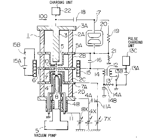
Referring now to Figs. 1 and 2, a vacuum switch
apparatus according to a first embodiment of the
201~64~
1 invention will be described. Generally designated at
reference numeral 100 in Fig. 1 is a vacuum switch
having the following construction.
The vacuum switch 100 has a vacuum enclosure 1
comprised of four stacked insulating cylinders 2A to 2D,
flanges 3A and 4A respectively connected to the outer
ends of the insulating cylinders 2A and 2D, and an
insulating member 4B connected to the outer end of the
flange 4A. Connected to the insulating member 4B is
a vacuum pump 5. The interior of the vacuum enclosure 1
is normally evacuated by means of the vacuum pump 5
and maintained at vacuum. The degree of the vacuum is
required to define a high vacuum condition of a vacuum
value which is higher, in terms of dielectric strength
in the Paschen curve, than the minimum. For example,
a high vacuum value of less than 2 x 10 Torr (2.66 Pa)
is needed. Unless the vacuum pump is normally used,
the interior of the vacuum enclosure may simply be evacuated
and the vacuum enclosure may be sealed airtightly for
use. Arranged inside the vacuum enclosure is at least
an anode electrode 3 to be described below.
The anode electrode 3 is secured to a central
portion of the flange 3A and it extends toward a cathode
electrode 5. The cathode electrode 5 has a flange 5A
supportingly clamped by the insulating cylinders 2A and 2B.
The central cathode electrode 5 merges into the flange
5A and is formed into a cup-shape which surrounds the
anode electrode 3, thereby ensuring that the current
201~644
1 conduction area is enlarged to reduce the circuit
reactance. The anode and cathode electrodes 3 and 5 are
made of, for example, a material of tungsten type copper
alloy which is less consumed under arcing or a material
of chromium type copper alloy which has a good breakdown
voltage characteristic.
A control electrode 6 is supportingly clamped
by the insulating cylinders 2B and 2C to oppose both of
the cathode electrode 5 and an electron current draw
electrode 7. The electron current draw electrode 7 has
a flange 7A supportingly clamped by the insulating
cylinders 2C and 2D and extends toward the control elec-
trode 6. Arranged inside the electron current draw
electrode 7 is an electron current control electrode 4.
The electron current control electrode 4 merges into
the flange 4A and extends toward the electron current
draw electrode 7 to form a space in which a filament
8 is arranged.
The opposite ends of the filament 8 pass through
through-holes formed in the flange 4A and they are
supported in the insulating member 4B so as to be exposed
to the outside. A beam 10 of electrons emitted from
the filament 3 and directed in a direction of arrow
travels through apertures 200 formed in the control
electrodes 4, 7, 6 and 5 to irradiate the anode electrode
3. The filament 8 and the electrodes 3, 5, 6 and 7 are
connected at least to power supplies provided externally
of the vacuum enclosure.
2011644
More particularly, the electron current draw
electrode 7 and electron current control electrode 4 are
connected through electric wires llA to a power supply 7X
for electron current draw and a power supply 4X for electron
current control, respectively, and the filament 8 is
connected through an electric wire 11 to a power supply 8X
for filament. The control electrode 6 is connected to one
end of a secondary winding 14 of a pulse transformer 12 and
a magnetic field generation coil 15 is provided to surround
the insulating cylinders 2B and 2C. The magnetic field
generation coil 15 is fed from a DC power supply 15A through
a switch 15B.
The pulse transformer 12 includes a primary winding
13 and the secondary winding 14. Connected across the
primary winding 13 are a capacitor 13A, a pulse switch 13B
and a pulse charging unit 13C, with a junction between the
capacitor 13A and switch 13B grounded. Used as the pulse
switch 13B is an SIT (an acronym for electrostation
induction type transistor). With the pulse switch 13B
opened, the control electrode 6 is applied with a negative
potential and with the switch 13B closed, with a positive
potential. One end of the secondary winding 14 is connected
to charging resistor 14A and a negative bias capacitor 14B
which is grounded. The other end of the secondary winding
14 is connected to the control electrode 6 as described
previously and to a main circuit, generally designated at
reference numeral 17, through a potential capacitor 16.
-- 8 --
20116~
1 The main circuit 17 is connected between the
anode electrode flange 3A and cathode electrode flange
5A through a capacitor 18 and a laser oscillator 20.
A resistor 19 is connected in parallel with the oscillator
20 and connected to the main circuit 17, and a resistor
21 is connected at one end to a junction between the
oscillator 20 and resistor 19 and at the other end
grounded. A charging unit 22 is connected to both the
capacitor 18 and flange 3A.
The vacuum switch 100 is turned on and off as
described below.
Firstly, the filament 8 is supplied with a
positive potential from the filament power supply 8X and
heated to emit an electron beam 10. Radial spreading of
the electron beam 10 is suppressed by means of the
electron current control electrode 4 supplied with a
negative potential from the electron current control
power supply 4X. The electron current draw electrode
power supply 7X supplies a positive potential to the
electron current draw electrode 7.
To turn on the vacuum switch, the charging
unit 22 charges the capacitor 18 so that a high voltage
is applied across the anode and cathode electrodes 3
and 5. Then, the pusle switch 13B is closed to discharge
the capacitor 13A, with the result that a discharge
current flows through the primary winding 13 to induce
a voltage in the secondary winding 14, thereby applying
to the control electrode 6 a positive potential V as
201164~
1 shown at (A) in Fig. 4. At that time, discharge is
initiated as shown in Fig. 3.
More specifically, a current il of the electron
beam 10 occurs as shown at (A) in Fig. 4 and passes
through the aperture in the cathode electrode 5 to heat
the anode electrode 3 (see section (A) in Fig. 3). The
electron beam collides with metal vapor particles emitted
from the surface of the heated anode electrode 3 (see
section (B) in Fig. 3) to ionize the metal vapor
particles, generating plasma (see section (C) in Fig. 3).
Thus, while colliding with each other, electrons and
positive ions are drawn to the anode electrode and the
cathode electrode, respectively, to render the switch
conductive (see section (D) in Fig. 3). At that time,
the switch is started to operate with a discharging
current i2 as shown at section (A) in Fig. 4 flowing
through the main circuit 17.
To turn off the vacuum switch, the pulse switch
13B is opened so that the control electrode 6 assumes a
negative potential (-VO) as shown at (A) in Fig. 4.
Consequently, the current il of the electron beam 10
falls to zero and irradiation of the electron beam 10 is
stopped (see section (E) in Fig. 3). Then, as the
discharge current i2 in the main circuit 17 falls to zero,
the generation of plasma between the anode and cathode
electrodes is stopped (see section (F) in Fig. 3).
Because of the plasma region being surrounded by the
vacuum environment, the residual electric charge diffuses
-- 10 --
20116~4
1 instantaneously (see section (G) in Fig. 3) and electrical
insulation between the anode and cathode electrodes
recovers (see section (H) in Fig. 3).
As described above, in the present invention,
because of the vacuum environment prevailing between the
anode and cathode electrodes before initiation of
discharge, the electron beam 10 can irradiate the anode
electrode surface rapidly without being scattered to
generate metal vapor particles which in turn are ionized
to form plasma. Consequently, discharge can be initiated
rapidly through the main circuit 17, thereby minimizing
discharge jitter. After discharge, the metal vapor
particles and plasma rapidly diffuse from the discharge
space into the vacuum environment, thus expiditing rapid
recovery of electrical insulation and rapid initiation of
the next discharge. Accordingly, the vacuum switch of
the present invention permits a great number of switching
operations at a high repetition rate within a short
period of time.
More specifically, by controlling the electron
beam irradiation time such that, as shown at (B) in
Fig. 4, the electron beam 10 is irradiated during an
interval of tiems which is slightly shorter than a
half-wave period of the discharge current i2 in the
main circuit 17 to permit early occurrence of the zero
point of discharge current i2 at which the discharge
current is intercepted, the high repetition rate switching
operation can be ensured.
2011644
1 Further, arc voltage for discharge between the
anode and cathode electrodes 3 and 5 in vacuum is far
smaller as compared to that for discharge in a gas atmos-
phere and therefore the amount of energy drawn to the
electrodes, that is, the product of current and arc
voltage can be small. In addition, the metal used for
the anode and cathode electrodes 3 and 5, for example,
tungsten/copper alloy or chromium/copper alloy is less
consumed and effective to prolong the life. For the
above reasons, the number of switching operations can
further be increased.
In this respect, expriments conducted by the
present inventors showed that when in the conventional
thyratron illustrated in Fig. 10, a voltage of less
than 20 KV was applied across the anode and cathode
electrodes to cause the flow of a discharge current of
less than 1 KA therebetween, switching was effected
only at 106 or less shots of discharge current. Contrary
to this, when in the vacuum switch of the present
invention, a rated voltage of more than 20 KV was applied
across the anode and cathode electrodes 3 and 5 to
cause the flow of a discharge current of more than 1 KA
therebetween, switching could be effected at 106 or
more shots of discharge current. Experimentally, switching
operation was also carried out at the rated voltage and
the maximum value of discharge current. The results
showed that when a rated voltage of 30 KV was applied
across the anode and cathode electrodes and the flow of
2011644
1 a discharge current of 10 KA was caused therebetween,
discharge current could be switched at 103 shots
according to the invention.
It should also be noted that in the foregoing
embodiment, the magnetic field generation coil 15 is
used to generate an axial magnetic field by which the
electron beam 10 can be condensed axially for irradiation
on the anode electrode without being scattered. This
leads to efficient use of the electron beam 10 which
improves efficiency of the filament 8 and consequently
reduce the size of the filament 8 per se and the power
supplies 4X, 7X and 8X.
In the foregoing embodiment, current is normally
passed through the magnetic field generation coil 15.
But in an alternative, the switch 15B may be turned on/off
in synchronism with turn on/off of the pulse switch 13B.
For example, the switch 15B may be opened in synchronism
with opening of the pulse switch 13B to stop the flow of
current in the magnetic field generation coil 15, thereby
suppressing power consumption. Conversely, if the
switch 15B is closed in synchronism with closure of
the pulse switch 13B to permit the flow of current in
the coil 15 on condition that current loss in the coil
15 is constant, the maximum permissible current can be
made greater in the case of the pulsed or intermittent
flow of applied current than in the case of the constant
flow of current. Thus, by passing a large amount of
current intermittently through the coil, intensity of an
- 13 -
201164~
1 induced magnetic field can be increased to thereby
increase electron density of the electron beam 10, thus
contributing to stabilization of the high repetition
rate discharge.
Referring to Figs. 5 to 9, vacuum switches
according to second to sixth embodiments of the invention
will now be described.
Fig. 5 shows a vacuum switch according to the
second embodiment of the invention wherein a magnetic
field generation coil 15 is arranged in a vacuum
enclosure. Advantageously, since in this second embodi-
ment the magnetic field density is strengthened on the
center axis, the density of beam current can be increased
to further improve stability of discharge control.
Fig. 6 shows a vacuum switch according to
the third embodiment of the invention. In this third
embodiment, an anode electrode 3 is attached to a flange
23 through the medium of a bellows 60 to make variable
the length of a gap between the anode electrode 3 and a
cathode electrode 5. With this embodiment, the breakdown
voltage characteristic can be improved to about 15 KV/mm.
With the gap length increased, when the amount of the
electron beam supplied from an electron beam source 24
is increased, stability of discharge can be increased.
In accordance with this embodiment, a vacuum switch of
100 KV class can be provided.
Fig. 7 shows a vacuum switch according to the
fourth embodiment of the invention wherein there are
- 14 -
20116~4
1 provided a plurality of electron beam sources 24 and
a plurality of apertures 25 so formed in a cathode
electrode 5 as to oppose an anode electrode 3. In this
fourth embodiment, electron beams are emitted alternately
from the different sources so that consumption of the
anode electrode 3 may be mitigated to prolong the life
of the vacuum switch.
Fig. 8 shows a vacuum switch according to
the fifth embodiment of the invention wherein plasma
generation can be amplified by secondary electrons. In
accordance with this fifth embodiment, an electron beam
10 emitted from an electron beam source 24 is deflected
from the emission direction under the influence of a
magnetic field 25 directed vertically to the sheet of
drawing to bombard the surface of an anode electrode 3
and vaporize the same. On the other hand, part of
electrons of the electron beam failing to be defected
will bombard the surface of a cathode electrode 5
and generate secondary electrons 26. The thus generated
secondary electrons collide with metal vapor particles
to amplify generation of plasma. It is to be noted
that in Fig. 8, the electron beam source 24 is attached
to a vacuum enclosure 1 above the cathode electrode 5
and the electron beam is irradiated obliquely on the
anode electrode.
While in any of the foregoing embodiments the
vacuum switch has been described as applied to the
laser apparatus, a vacuum switch may be applied to a soft
2011644
1 X-ray source of plasma focus type as shown in Fig. 9
according to the sixth embodiment of the invention.
In this sixth embodiment, a rare gas (Ne, Ar,
Kr and so on) is filled in a vacuum enclosure 30.
Electric charge stored in a capacitor 33 is applied across
concentric electrodes 31 and 32 through a vacuum switch
100. At that time, discharge starts along the top surface
of an insulator 34 and a discharge sheath then runs
downwards with the result that plasma pinches in the
front of the electrode 31 and soft X-rays 35 due to the
high temperature and high density plasma are generated
from the electrode 31. In an application of X-ray
lithography, the thus generated soft X-rays 35 transmit
through a transmission window 36 and a pattern defined by
a mask 37 is transferred to a silicon wafer 38. Denoted
by 39 is an aligner. The soft X-ray source requires a
discharge current of several hundreds of KA.
The vacuum switch of the present invention can
be applied to a soft X-ray source and a neutron source
which utilize a large current plasma pinch, a plasma gun
for shooting a spatial lump of plasma at an initial
velocity of about 105 m/s, an electromagnetic accelerator
for accelerating a flying object of several grams to
several kilo-grams, a uranium enriching system and the
like. For example, in an application to the uranium
enriching system wherein a uranium metal having uranium
isotopes 235 and 238 is placed in a vacuum enclosure and
the uranium metal is vaporized to produce rising metal
- 16 -
2011~
1 vapor particles on which a laser beam emitted from a
laser oscillator is irradiated, the vacuum switch of the
present invention may be used to on/off control the
irradiation of the laser beam on the metal vapor particles
for the sake of controlling separation of the metal into
uranium isotopes 235 and 238.
~ ccording to the invention, there is provided
an apparatus in which at least one set of opposing anode
and cathode electrodes is arranged in the vacuum enclosure
and an electron beam is irradiated on the surface of
the anode electrode. With this construction, because of
the vacuum environment, the electron beam can be controlled
properly so that the anode electrode surface can be
vaporized under the bombardment of the electron beam to
produce metal vapor particles which are irradiated with
the electron beam to form plasma, thereby ensuring high
repetition rate control of switching and high voltage
operation.