Note: Descriptions are shown in the official language in which they were submitted.
201825
64159-1130
METHOD AND APPARATUS FOR GENERATING DISPLAY
FIGURES WITH THREE DEGREES OF FREEDOM
U. S. GOVERNMENT RIGHTS
The United States Government has contributed to the
design and development of the invention disclosed herein and has
certain rights thereto.
BACKGROUND OF THE INVENTION
The invention is directed generally to a method and
apparatus for constructing figures on a display device and, more
particularly, to a method and apparatus for constructing figures,
such as lines, arcs, and curves using chained three dimensional
unit vectors for drawing characters, symbols, and wireframe
objects on a display device such as a CRT screen.
Display devices are used to convey information for
many applications. In one application, advanced cockpit concepts
use helmet mounted display devices to convey information to
aircraft pilots. The information presented on such a display
must be stabilized due to variations in the helmet and aircraft
pitch, roll, and yaw motions. A large computational overhead is
associated with the three dimensional nature of the required
stabilization. Currently standard rotation algorithms in
computer software are used to provide such stabilization. In
addition to the stabilization requirements, human factor studies
have shown that helmet mounted displays require a higher update
rate than conventional head-down display and head-up display
devices. Consequently, more computationally intensive informa-
tion must be displayed in a shorter amount of time than is
-1-
2011825
64159-1130
presently feasible using current devices.
Current display processors construct display formats
with two dimensional vectors using a Cartesian coordinate data
base. These vectors can use various rotation computer algorithms
in computer software to stabilize the image. Unfortunately, the
algorithms implemented in software are too slow to meet system
requirements for applications such as helmet mounted displays.
-la-
2011825
-a __
Co-processors have been used to increase the computational
efficiency of processors using such software. However, the use
of co-processors does not significantly improve the time
consuming rotation algorithms currently used to calculate each
x,y point on a Cartesian grid. More computationally efficient
data signal processors and data signal processor modules have
successfully closed the gap on the time required to compute the
x,y points, but have not provided the high update rates required
for cockpit display applications.
The invention provides a solution to the above-described
computational problem because it does not require the processor
to use a rotation algorithm to calculate each x,y point. The
invention allows the processor to work at a higher level of
abstraction without incurring time delays by handling the
computational aspects of generating a display. This higher level
of abstraction is gained by using polar vectors as building
blocks to create straight lines, circular arcs, and arbitrary
curves (such as Bezier curves). The abstraction is achieved by
virtue of the method in which the three dimensional rotation
equations are utilized by the invention. Th~ method uses a unit
vector along the x-axis rotated about the z-axis and then about
the y-axis. Varying the rotations provides two functions:
(a) Construction of any line, any arc, or any curve in
three space; and
(b) orientation of the constructed line or arc in any
direction in three space.
In constructing display formats using the invention, a processor
is required to specify only the size, orientation, and location
of objects. The processor can then be used to manage the display
- ~~- 2o~~sz~
format and is not required to process the point-by-point drawing
of the display format.
It is one object of the invention to balance hardware and
software tasks to efficiently construct display formats that
require high throughput and image stabilization.
One advantage of the invention is that it allows objects
to be created off-line as three dimensional icons and prestored
symbols.
It is yet another advantage of the invention that display
format objects created using the invention have the inherent
ability to be rotated, translated, and scaled.
Yet another advantage of the invention is that the method
of the invention is well suited for implementation in a pipeline
architecture resulting in increased system throughput as compared
to prior art systems.
Yet another advantage and feature, of the invention is
that the display processor is not loaded by the computationally
intensive display generation task as in prior art systems.
Yet another advantage of the invention is that display
figures may be occluded with display processors implementing a
Z-buffer device.
Yet another advantage of the invention is that display
figures may be displayed with depth cuing for display processors
that implement a depth cuing function using the Z-values
resulting from the invention.
Other objects, features and advantages of the invention
will become apparent to those skilled in the art through the
claims, description and drawings herein wherein like reference
numerals refer to like elements.
64159-1130
2011825
SUMMARY OF THE INVENTION
An apparatus and method we disclosed for providing x,
y and z values so as to construct figures from unit vectors
rotated in three space wherein the x, y and z values result
from processing construction and global rotation parameters
according to the following relationships:
O X~ = L~ X COS (GZ) + Q Y SIN (GZ)
O y~ - - D X SIN(GZ) + O Y COS (GZ)
Q Z~ = Q Z
where,
D X ' COS ( RZ ) COS ( Ry + Gy )
D Y = COS(RZ) SIN(RY + Gy) SIN(GX) - SIN(RZ) COS(Gx)
O Z = COS(RZ) SIN(Ry + Gy) COS(GX) + SIN{RZ) SIN(GX)
and,
RZ, and Ry are construction rotation parameters and Gy, GX and GZ
are global rotation parameters for the rotation about the X, Y
and Z axes.
As used in a graphics display system, the invention
provides offset values to a means for summing offset values
from a specified point. Means for providing depth cuing
related to the offset values may be advantageously included in
an alternative embodiment for apparatus employing the
principles of the invention. Processed x, y and z values,
together with color cuing information may then be stored in a
memory prior to displaying the figure.
In accordance with the present invention, there is
provided a three dimensional vector generator apparatus
including a data bus, wherein the three dimensional vector
generator comprises: (a) a first programmable array logic block
means having an input connected to the data bus and having an
._' 4
..--
64159-1130 2 01 18 2 5
output; (b) a first adder means having a first input connected
to the output of the first programmable array logic block
means, and further having a second input and an output; (c) a
second programmable array logic block means having a first
input connected to the output of the first adder means, having
a second input connected to the data bus and having an output
connected to the second input of the first adder means; (d) a
first sine/cosine PROM means having an input which is also
connected to the output of the second programmable array logic
block means and further having an output; (e) a first
deflection accumulator means having first, second, and third
inputs and having an output, wherein the third input is
connected to the output of the first sine/cosine PROM means;
(f) a first feedback circuit means having an input connected to
the output of the first deflection accumulator means and having
an output fed back to the third input of the first deflection
accumulator means; (g) a third programmable array logic block
means having an input connected to the data bus and having an
output; (h) a second adder means having a first input connected
to the output of the second programmable array logic block
means, and further having a second input and an output; (i) a
fourth programmable array logic block means having a first
input connected to the output of the second adder means, a
second input connected to the data bus and having an output
connected to the second input of the second adder means; (j) a
second sine/cosine PROM means having an input which is also
connected to the output of the fourth programmable array logic
block means and further has an output connected to the second
input of the first deflection accumulator means; (k) a second
deflection accumulator means having first, second, and third
inputs and having an output, wherein the third input is
connected to the output of the first sine/cosine PROM means;
(1) a third sine/cosine PROM means having an input which is
also connected to the output of the fourth programmable array
4a
~,r_.
64159-1130
2011825
logic block means and further has an output connected to the
second input of the second deflection accumulator means; (m) a
second feedback circuit means having an input connected to the
output of the second deflection accumulator means and having an
output fed back to the second input of the first deflection
accumulator means; (n) a register means having an input
connected to the output of the second deflection accumulator
means and an output connected to the second input of the second
deflection accumulator means; (o) a plurality of output
register means including first, second, and third output
registers with each output register having an input and an
output, wherein the input of the first output register is
connected to the output of the first deflection accumulator
means and the inputs of the second and third output registers
are connected to the output of the second deflection
accumulator means; and (p) means for controlling elements (a)
through (o) having a plurality of control lines including a
first control line connected to the data bus so as to provide
control signals to the elements (a) through (o) so as to
produce Cartesian coordinate offsets for unit vectors at the
outputs of the first, second and third output registers.
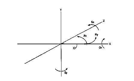
BRIEF DESCRIPTION OF THE DRAWINGS
Figure 1 illustrates a unit vector oriented along the
x-axis in three space and defines the rotation parameters.
Figure 2(a) illustrates a line constructed by varying
Ry and RZ for each unit vector.
1
4b
_ - ~ - 201182
Figure 2(bj illustrates a line constructed with Ry = RZ =
0 and varying Gy and GZ.
Figure 2(c) illustrates an example of a polygon
constructed by varying Rz.
Figure 3 is an illustration of a functional block diagram
of an embodiment of the invention.
Figure 4 is a system block diagram showing an example of
a system employing features of the invention.
Figure 5 is a circuit diagram of one example of an
embodiment of the invention.
Figure 6 is an example of a compass rose.
DESCRIPTION OF THE PREFERRED EMBODIMENT
Referring now to Figure l, the rotation of the unit
vector in three space is illustrated graphically. The method and
apparatus of the invention for drawing three dimensional symbols
and characters is based upon construction and rotation of a unit
vector 10 oriented along the x-axis in three space as shown in
Figure 1. Those skilled in the art will recognize that the x, y,
z three space convention used in this description is used by way
of an illustrative example. Other conventions may be used and
will yield similar results using the methods and apparatus of the
invention. However, for ease in explaining the invention, the
convention for three space shown in Figure 1 will be used
throughout this description of the invention with the
understanding that the invention is not limited to use with this
particular convention.
Given a unit l0 in three space placed along the positive
x-axis, then any three dimensional wireframe figure may be
constructed by concatenating a series of such unit vectors after
rotating each vector first about the z-axis and then about the
-.-~- 201125
y-axis. Once a wireframe figure is constructed with a series of
rotated unit vectors, the wireframe object may be then
manipulated by the steps of:
(a) Change in the starting point for translation,
(b) Adding a constant to the x-rotation value for
rotation about the x-axis,
(c) Adding a constant to the y-rotation value for
rotation about the y-axis, and
(d) Adding a constant to the z-rotation value for
rotation about the z-axis.
The mathematics used to construct and manipulate the
wireframe object is given by the following equations:
Q X~ = Q X COS(GZ) + Q y SIN(GZ)
OY~ _ - ~ X SIN(GZ) +Q Y COS (GZ)
Q Z~ = 0 Z
where,
D X = COS ( Rz ) COS ( Ry + Gy )
D Y = COS(Rz) SIN(Ry + Gy) SIN(Gx) - SIN(Rz) COS(Gx)
O Z = COS(Rz) SIN(Ry + Gy) COS(Gx) + SIN(RZ) SIN(Gx)
and,
Rz, and Ry ara construction rotation param~ters about the Z and Y
axes, respectively, and Gy, Gx and Gz are global rotation
parameters for the Y, X and Z axes, respectively. The equations
above are used to calculate the points defining the unit vectors
as constructed by the method described above. An important
feature of this method is the order of rotation.
Figure 2(a) illustrates a line comprised of unit vectors
10 wherein the line is constructed by varying Ry and Rz for each
unit vector. The vectors 10 may be rotated about the z-axis and
then the y-axis to achieve any orientation. Once an orientation
_ - ~ - 2011825
is chosen,. the vectors 10 may be replicated any number of times
to construct a line "'n" units long where "n"' represents any
integer. An alternative method for displaying a line is shown in
Figure 2(b). The line is constructed by varying Gy and Gz with
Ry = RZ = 0.
A curve or an arc may be constructed if a vector is
replicated n number of times with a new orientation specified
each time. Figure 2(c) shows an octagon 20 in three space
constructed of unit vectors 10 wherein the octagon 20 has been
constructed by varying Rz. Note that finer rotation angles about
z would, give better approximations of a circle. The size of an
object is controlled by the number of times a unit vector for a
given orientation is repeated. In addition to the rotation of a
unit vector in three space, the invention uses global rotation
parameters to rotate lines, arcs, and curves as a whole. The
global rotation parameters can also be used to rotate multiple
lines, arcs and curves for symbol or character rotation in three
space. Using global rotation parameters, therefore, one can
store predefined characters in a programmable read-only memory
(PROM), for example, read those characters out of memory and
display them on a screen at any given rotation in three space.
Figure 3 is an illustration of a functional block diagram
of one embodiment of the computer algorithm of the invention
depicting the order of operations for calculating the x, y and z
points. In general, the calculation proceeds from a polar
description to Cartesian coordinate offsets,, X', ~ Y' and ~ Z'.
The offsets are accumulated from a starting point defined by
construction parameters Rz and Ry and rotation parameters Gy, GX
and Gz. The offsets are accumulated from a starting point to
give the_ coordinate position of the point on the display device
64159-1130
to be illuminated. Still referring to Figure 3, once the
instruction has been decoded, the construction and rotation
parameters are loaded into the three dimensional vector
generator 30. Because of the order of rotation, the y-
construction and rotation values may be added together first.
The sum of the y-values along the with z-construction and x-
rotation parameters are then presented to the sine/cosine look-
up tables 32 and 34, respectively. The sine/cosine look-up
tables may advantageously be PROMs of the type which are well
known in the art. The outputs from the mathematical first
stage 36, as shown by the dotted line are x, y and z offset
values. At this point the values construct an object in three
space rotated in x and y only. The z-rotation parameter, GZ, is
used in the next state 38 of sine/cosine tables to retrieve the
z-rotation values. The last stage of mathematics 40 produces
the final ~ X~, 0 y~ and, Z~values for an object rotated in
three space.
Figure 4 is a system block diagram showing an example
of a video display system employing the features of the
invention. The system comprises a character font PROM 50, a
dual port interface 52, a front-end controller 54, a 3D vector
generator 30, sine/cosine PROMs 31, deflection accumulator 56,
color look-up table 58, full frame memory 60 and a video bus
62. An instruction list is provided to the system by the
display processor 70. The list is accessed and decoded through
the interface 52 by the front-end controller 54. The front-end
controller 54 may be any type of well-known processor, such as
a microprocessor device or programmable gate array or other
programmable logic device. When the display processor 70 is
required to display a character or user defined symbol, the
controller accesses the character font PROM. The character
. font
8
- c~, .~. 2 0118 2
PROM is loaded with predefined characters and fonts by the user
of the system as required. Those skilled in the art will
appreciate that the use of such character font PROMs are well
known. The concatenation of the instruction and character font
lists are then transmitted to the three dimensional vector
generator 30 for processing. As the three dimensional vector
generator processes the information, the offset values are summed
in the deflection accumulator which tracks the current position.
Preloading the deflection accumulator 56 with a predetermined
point on the display device has the effect of translating the
object. In other words, the offset values generated begin
accumulating from the predetermined point on the screen. In the
case of a color display, a color look-up table may advantageously
be used to provide depth cuing with any color. Depth cuing is
accomplished by modulating intensity as a function of Z-depth,
thereby rendering farther objects as having dimmer intensities.
The output from the color look-up table 58 is stored in a full-
frama memory 60 based on the values of the x, y outputs. Of
course, in the case of a monochrome display screen, the color
look-up table is not required. The full-frame memory may be
advantageously any high speed memory device suitable for video
display applications. The full-frame memory 60 is scanned by a
digital video bus s2 or digital-to-analog conversion and
subsequent presentation on the display 100.
Referring now to Figure 5, a more detailed circuit
diagram of one example of an embodiment of the invention is
shown. Terms and signal names used in Figure 5 are defined in
Table I.
TABLE I
Term Definitions for The 3D Vector Generator
- 10 - 201182
....--
Register Load
LRZ* (Load Relative Z register) -- Loads a 12 bit register
with data which is used as a starting rotation angle
about the Z axis.
LRY* (Load Relative Y register) -- Loads a 12 bit register
with data which is used as a starting rotation angle
about the Y axis.
LDZ* (Load Delta Z register) -- Loads a 12 bit register
with data which is used as a 0 to the Z rotation
angle.
LDY* (Load Delta Y register) -- Loads a 12 bit register
with data which is used as a 0 to the Y rotation
angle.
LGZ* (Load Global Z register) -- Loads a 12 bit register
with data which applies a global Z rotation angle to
all vectors drawn subsequent to the load.
LGY* (Load Global Y register) -- Loads a 12 bit register
with data which applied a global Y rotation angle to
all vectors drawn subsequent to the load.
LGX* (Load Global X register) -- Loads a 12 bit register
with data which applies a global X rotation angle to
all vectors drawn subsequent to the load.
LEN* (Load Length Register) -- Loads a 12 bit register
with a repeat value for the length of the current
vector. This register load causes execution of a
vector draw.
Control Inputs
SELECT* (Draw Select) -- Activates the output registers of
the vG permitting reading of the results.
READY* (Output Ready) -- Indicates the controller is
finished with the currant results of the VG and
permits the VG to proceed.
Internal Control Terms
OEA* (Output Enable for X & Y) -- Allows forward flow of
data to the DACs when low and feedback when high. It
is changed by the state controller as required to
implement the equations specified.
oEB* (Output Enable for Z) -- Allows forward flow of data
to the DACs when low and feedback when high. It is
changed by the state controller as required to
implement the, equations specified.
FLA* (Feedback Latch Enable) -- Used to save required
terms for the X & Y feedback path.
.,
64159-1130 2 01 18 2 5
OSA* (Feedback Select X & Y) -- Used to pick the feedback
path or the saved feedback term as required by the
equations.
EXE* (Execute Instruction) -- Control signal from the
state controller is used to begin a draw instruction.
This instruction results in loading of all registers
into the VG operations area.
ACU* (Accumulate Z Terms) -- Permits the Z angla register
to accumulate the current angle with the ~ Z angle.
This is done at the end of each step in a vector
draw.
ACC* (Accumulate Y Terms) -- Permits the Y angle register
to accumulate the current angle with the ~ Y angle.
This is done at the end of each step in a vector
draw.
SGR* (Exchange Z Terms) -- Permits the exchange of the
current Z direction with the Global Z direction when
needed.
SXY* (Exchange X & Y Terms) -- Permits the exchange of the
current Y direction with the Global X direction when
needed.
SIN/COS* (Sine/Cosine Select) -- Selects the sine or cosine
values from the PROM lookup tables as needed for
each input term.
OAC* (Output Accumulate) -- Permits the state controller
to enable an accumulation of the prior product terms
with the current product terms as required by the
equations.
;i
11
64159-1130 2 01 18 2 5
~.
LXR* (Load X Result register) -- Permits the state
controller to save the X result when it becomes
available.
LYR* (Load Y Result register) -- Permits the state
controller to save the Y result when it becomes
available.
LZR* (Load Z Result register) -- Permits the state
controller to save the Z result when it becomes
available.
The embodiment of the invention shown in Figure 5
comprises a first programmable array logic block (PAL) 200, a
first adder 202, a second programmable array block 204,
sine/cos PROM 206, a first feedback circuit 208, a second
feedback circuit 210, a register 212, and output registers 220,
222, and 224. A third input programmable array logic block 230
is provided, as is a second adder 234, and a fourth
programmable array logic block 236. Second and third
sine/cosine PROMS 240 and 242 are also provided. Output
multiplier/accumulators 250 are also included in the last
stages of the circuit. The three dimensional vector generator
shown in Figure 5 is controlled by state controller 300 and the
components are connected through a plurality of data buses 310.
Having described generally the elements comprising
the embodiment of the invention shown in Figure 5, an example
of the invention in operation will now be described in order to
aid in understanding the invention.
Under the control of state machine 300, instructions
transmitted on data bus 310 are decoded and the appropriate
enable signals are transmitted onto the pipeline. All enable
signals are controlled based on the state of the three
dimensional vector generator and the decoded instructions.
12
64159-1130 2 01 18 2 5
This control is required to set up the correct data at the
inputs of the arithmetic units 202 and 234 at the correct time.
In operation, programmable array logic block 200, which
includes registers 102 and 104, where register 102 is connected
to the data bus 310 and comprises a 12 bit register used to
provide an incremental change to the z-rotation angle. The
output of register 102 is connected to the input of register
104 which loads information passed from register 102 into adder
202 in response to the execute instruction, EXE*. Adder 202
then takes data into its B-input and sums it with data from its
A-input to supply the sum of ~ z plus information fed back
from PAL 204 and data bus 106. PAL 204 is further comprised of
a plurality of registers and flip-flops configured in a way to
perform data pipeline operations in response to the LGZ*, ACU*,
EXE* and SGR* functions. The output of PAL 204 is then
processed as an address ..
g'
12a
~0118~5
input to sine/cos PROM 206 which, in response to the OEB* control
signal, then allows forward flow of data to the deflection
accumulators 250A and 250H. The deflection accumulators perform
multiplication and addition operations as shown. The deflection
accumulators further respond to the output accumulate control
signal, OAC*, which enables an accumulation of the prior product
terms with the current product terms as required by the equation.
The output of accumulator 250A is loaded into the Z output
register 220 and also fed back through feedback amplifier 208 to
the input of 250A and an input of 250B. The remaining components
operate in a~similar manner in response to the control signals as
outlined in Table I.
An example of constructing a compass rose using the
method of the invention is presented in Figure 6. The
instruction list for constructing this object is shown below
together with execution times for implementing the series of
instructions using the method of the invention. This is an
example of the type concatenated list described hereinabove with
reference to the figures. The time associated with the three
dimensional vector generator (3DVG) implementation column is
based on a 12.5 MHz system clock. Following the 3DVG
implementation list is a list entitled "'A Polyline
Implementation". The polyline implementation list is one that
might be used with a prior art display processor using the
Programmer's Hierarchical Interactive Graphics Standard. The
times associated with the polyline implementation column are
based on using a Type 68030 microprocessor using a 25 MHz clock.
Note that the comparison does not include rotating the image.
Since rotation is embedded into the 3DVG, there is no more
calculation required to rotate the image. The polyline
_~z_
_ -I~ ~ 2011825
implementation would have to add a rotation algorithm to rotate
the image. Therefore, the
processor implementation
throughput
would decrease at least an order of magnitude due to the
increased multiplications, additions, subtractions, and table
look-ups. In the case of this example, the 3DVG provides nearly
two orders of magnitude total improvement if rotation is
considered, and nearly one order of magnitude total improvement
if no rotation is considere d.
3DVG IMPLEMENTATION
SLEW
(O, O, -512)
COLOR/SCALE (27, RGB)
Z - DIR ( 0 )
LENGTH (8) : 0.64 us
Z - DIR (-pl/2)
LOOP CNT (48) : 42.24 us
dZ - DIR (-pl/32)
LENGTH (4)
dZ - DIR (31p1/64)
LENGTH (1)
dZ - DIR (pl)
LENGTH (l, blank)
dZ - DIR (31p1/64)
JUMP NZ REL (-7)
dZ - DIR (0)
Z - DIR (3p1/2)
COLOR/SCALE (9, RGH)
LENGTH (34,blank) : 2.96 us
Z - DIR (-pl/2)
LENGTH (48) : 3.92 us
Z - DIR (3p1/2)
-1d-
211825
LENGTH (34,blank) : 2.80 us
Z - DIR ( 0 )
LENGTH (24) : 2.00 us
Z - DIR (-pl/128)
LENGTH
(27,blank) 2.16 us
JUMP ABS ('E') : 3.20 us
Z - DIR (pl)
LENGTH (55) : 4.48 us
JUMP ABS ('W') : 3.20 us
Z - DIR (pl/4)
LENGTH (40) : 3.28 us
JUMP ABS ('N') : 3.20 us
Z - DIR (-31p1/64)
LENGTH (54) : 4.40 us
JUMP ABS ('S') , : 3.20 us
:81.68 us
TOTAL TIME
A POLYLINE IMPLEMENTATION
Circle:
POLYLINE (48 pts)
Tick Marks:
POLYLINE ( 2 pts )
POLYLINE (2 pts)
POLYLINE (2 pts)
POLYLINE (2 pts)
201182
POLYLINE (2 pts)
POLYLINE (2 pts)
POLYLINE (2 pts)
POLYLINE (2 pts)
POLYLINE ( pts
2 )
POLYLINE (2 pts)
POLYLINE (2 pts)
POLYLINE (2 pts)
POLYLINE ( pts
2 )
POLYLINE (2 pts)
Characters:
POLYLINE (16 pts) ('S')
POLYLINE (5 pts) ('W')
POLYLINE (4 pts) ('N')
POLYLINE (7 pts) ('E'),
19 command reads ~ 209 cycles
108 vertex reads p 2268 cycles
108 vector conversions p 7020 cycles
756 writes @ 8316 cycles
712.5 us TOTAL TIME
In one embodiment of the invention PALs used for PAL 200
were Model Type 2-EP610 as manufactured by Alters. PAL 204 was a
Model Type 6-22V10 as manufactured by Cypress and accumulators
250 were MULT/ACC 7243 LSI chips as manufactured by IDT.
Registers used as output registers for x, y and were Model 2-'374
16 bit registers. The state controller was a Type PAL3-22V10.
~ 2011825
While the invention has been particularly shown and
described in detail with reference to the preferred embodiments
thereof, it will be understood by those skilled in the art that
changes in form and details may be made therein without departing
from the spirit and scope of the invention.
What is claimed is: