Language selection

Search

Patent 2012360 Summary

Third-party information liability

Some of the information on this Web page has been provided by external sources. The Government of Canada is not responsible for the accuracy, reliability or currency of the information supplied by external sources. Users wishing to rely upon this information should consult directly with the source of the information. Content provided by external sources is not subject to official languages, privacy and accessibility requirements.

Claims and Abstract availability

Any discrepancies in the text and image of the Claims and Abstract are due to differing posting times. Text of the Claims and Abstract are posted:

  • At the time the application is open to public inspection;
  • At the time of issue of the patent (grant).
(12) Patent: (11) CA 2012360
(54) English Title: POWER SUPPLY BACKUP CIRCUIT
(54) French Title: CIRCUIT D'ALIMENTATION DE SECOURS
Status: Deemed expired
Bibliographic Data
(52) Canadian Patent Classification (CPC):
  • 323/5
(51) International Patent Classification (IPC):
  • H02J 9/06 (2006.01)
(72) Inventors :
  • ISHII, TAKAAKI (Japan)
  • SAKANISHI, MASAYUKI (Japan)
(73) Owners :
  • KABUSHIKI KAISHA TOSHIBA (Not Available)
(71) Applicants :
(74) Agent: MARKS & CLERK
(74) Associate agent:
(45) Issued: 1995-08-01
(22) Filed Date: 1990-03-16
(41) Open to Public Inspection: 1990-09-16
Examination requested: 1990-03-16
Availability of licence: N/A
(25) Language of filing: English

Patent Cooperation Treaty (PCT): No

(30) Application Priority Data:
Application No. Country/Territory Date
64854/1989 Japan 1989-03-16

Abstracts

English Abstract


Improvements to a power supply backup circuit
used to backup the operation of a radio device or the like
when a power supply therefor is interrupted. A reverse
current preventing diode is connected such that its anode
is connected to the junction point of a DC power source
and a voltage stabilizing circuit, and a cathode connected
to the stabilizing circuit. A transistor is provided
which has a collector connected to the cathode of the
diode, an emitter connected to one end of a capacitor the
other end of which is grounded, and a base connected to a
DC power source via a first resistor, and which has a
second resistor connected across the base and emitter
thereof. A third resistor is further connected across the
collector and emitter of the transistor.


Claims

Note: Claims are shown in the official language in which they were submitted.


- 8 -

THE EMBODIMENTS OF THE INVENTION IN WHICH AN EXCLUSIVE
PROPERTY OR PRIVILEGE IS CLAIMED ARE DEFINED AS FOLLOWS:

1. A power supply backup circuit comprising:
a capacitor having a capacity large enough to backup
a load;
a charging circuit for charging the capacitor via
current limiting means;
a discharging circuit for supplying the stored
charges in the capacitor via switching means to a junction
point of reverse current preventing means and a voltage stabi-
lizing circuit;
means for detecting interruption of a current from a
DC power source; and
control means for turning on the switching means in
response to a detection output from the detecting means indic-
ative of the detection of interruption of the current from the
DC power source.
2. A power supply backup circuit according to claim 1,
wherein the switching means includes a transistor having a
base, a collector connected to the junction point of the re-
verse current preventing means and the voltage stabilizing
circuit, and an emitter connected to the capacitor;
the control means includes a circuit in which the DC
power source is connected to the base of the transistor via a
first resistor and in which a junction point of the emitter
and the base of the transistor connected via a second resis-
tor; and
the charging circuit includes a circuit for charging


- 9 -
the capacitor via the first and second resistors.
3. A power supply backup circuit comprising:
a first load connected directly to a DC power source
and requiring no backup;
a second load requiring a backup connected via a
reverse current preventing means and a voltage stabilizing
means to the DC power source;
a capacitor having a capacity large enough to backup
the second load;
switching means connected across the capacitor and a
junction point between the reverse current preventing means
and the voltage stabilizing means;
a charging circuit for charging the capacitor via
current limiting means; and
control means for turning on the switching means
when an electric current from the DC power source is inter-
rupted.
4. A power supply backup circuit according to claim 3,
wherein the charging circuit includes:
a first charging circuit for directly charging the
capacitor with an output of the DC power source; and
a second charging circuit for charging the capacitor
with the output of the DC power source via the reverse current
preventing means.
5. A power supply backup circuit according to claim 3,
wherein the reverse current preventing means includes a diode
having an anode connected to the DC power source and a cathode
connected to the voltage stabilizing circuit.


- 10 -
6. A power supply backup circuit according to claim 3,
wherein the switching means includes a transistor having a
base, a collector connected to a junction point of the reverse
current preventing means and the voltage stabilizing circuit,
and an emitter connected to the capacitor;
the control means includes a circuit in which the DC
power source is connected to the base of the transistor via a
first resistor and in which a junction point of the emitter
and the base of the transistor connected via a second resis-
tor; and
the charging circuit includes a circuit for charging
the capacitor via the first and second resistors.
7. A power supply backup circuit comprising:
a reverse current preventive diode having an anode
connected to a DC power source and a cathode connected to a
voltage stabilizing circuit;
a series connected circuit having a switching ele-
ment and a capacitor provided across the ground and the cath-
ode of the diode; and
current path means having a current limiting element
for leading a current from the DC source to a junction point
of the switching element and the capacitor;
whereby the switching element is turned off in
accordance with the potential of the current path means when
the capacitor is charged with the current from the current
path means, and turned on in accordance with a potential
caused by a discharging current from the capacitor to the
current path means when the current from the DC source is

- 11 -
interrupted, so that the discharging current from the capaci-
tor is fed to the voltage stabilizing circuit via the switch-
ing element thus turned on.
8. A power supply backup circuit comprising:
a reverse current preventing diode having an anode
connected to a DC power source and a cathode connected to a
voltage stabilizing circuit;
a capacitor with one end being grounded and having a
capacitor large enough to backup an object load; and
a transistor having a collector connected to the
cathode of the diode, an emitter connected to another end of
the capacitor and a base connected to the DC power source via
a first resistor, the base and the emitter being connected via
a second resistor.
9. A power supply backup circuit according to claim 8,
further including a third resistor connected across the col-
lector and the emitter of the transistor.


Description

Note: Descriptions are shown in the official language in which they were submitted.


2ol236o
-- 1 --
POWER SUPPLY BACKUP CIRCUIT


BACKGROUND OF THE INVENTION
1. Field of the Invention
The present invention relates to improvements to
power supply backup circuits used for backing up the
operation of the circuit, for example, of a radio device
when a power supply is interrupted.
2. Description of the Related Art
FIG. 1 is a circuit diagram of a conventional
power supply backup circuit. As shown, the circuit
includes a reverse current preventing diode 4 inserted
between a DC source 1 and a voltage regulator or
stabilizer 2 and a capacitor 3 having a capacity large
enough to backup a load 5 on the regulator 2, the
capacitor having one end connected to a line to which the
diode 4 and the regulator 2 are connected and the other
end grounded. A load 6 is a circuit the operation of
which does not require backup when the power supply is
interrupted temporarily.
In operation, when power supply is stopped, for
example, by an instantaneous interruption of the DC source
1, electric charges stored in the capacitor 3 discharge to
backup the operation of the load 5 for a predetermined
time. At this time, the current of electric charges to
the load 6 is prevented by the diode 4.
As the capacitor 3, a small-type large-capacity
tantalum electrolytic capacitor which is excellent in


2012360
-- 2


leakage current, frequency and temperature characteristics
tends to be used recently in accordance with a demand for
miniaturized high-density integrated electronic devices.
However, the tantalum electrolytic capacitor has
the problem that it is likely to be deteriorated due to
rapid charging and discharging,due to being subjected to
an excessive voltage or a reverse voltage and to be
destroyed due to a shorting mode. Since there is a set
load during discharging, there is no problem, but the
breakage of the capacitor is mainly caused by an excessive
current flowing therethrough during charging.
In order to cope this problem, one conceivable
attempt is to provide a resistor between the capacitor 3
and the junction point between the diode 4 and regulator 2
to limit the current chargi~g the capacitor 3. However
there occurs a new problem that during discharging, a
voltage available from the load 5 would be reduced due to
a voltage drop across the resistor in such arrangement.
As just described above, the capacitor 3 is
charged and discharged usi~g the single current path 11 in
the conventional power supply backup circuit, so that a
voltage available from the load 5 would be reduced by
inserting a resistor in the current path 11 to limit the
curren~ charging the capacitor 3.
Thus, the use of a tantalum electrolytic
capacitor suitable for high-density integration as the
capacitor 3 provides no enough voltage to the load if a


2012360
-- 3
measure to protect the capacitor during charging is
considered.

SUMMARY OF THE INVENTION
It is an object of the present invention to
provide a power supply backup circuit which is capable of
supplying enough voltage to a load even if a tantalum
electrolytic capacitor suitable for high-density
integration is used as the capacitor.
In order to achieve the above object, the
present invention provides a power supply backup circuit
comprising at least a reverse curre~t preventive diode
having an anode connected to a DC power source and a
cathode connected to a voltage stabilizing circuit; a
series connected circuit of a switching element and a
capacitor provided across ground and the cathode of the
diode; and current path means including a current limiting
element for leading a current from the DC source to the
junction point of the switching element and the capacitor;
whereby the switching element is turned off in accordance
with the potential of the electric path means when the
capacitor is charged with the current from the capacitor,
and turned on in accordance with a potential due to a
discharging current from the capacitor to the current path
means when the current from the DC source is interrupted,
such that the discharging current from the capacitor is
fed to the voltage stabilizing circuit via the switching
element turned on.


Z012360

By such arrangement, the charging current
flowing through the current path is limited by the current
limitter while the discharging current flowing through the
switching element is not limited. Therefore, it is
possible to provide enough voltage to the load even if a
tantalum electrolytic capacitor suitable for high density
integration is used.
Therefore, according to the power supply backup
circuit according to the present inventio~, a
deterioration in the performance of the capacitor which
would otherwise arise due to rapid charging a~d
discharging is prevented, so that enough voltage is
supplied to the load if a tantalum electrolytic capacitor
suitable for high density integration is used.


BRIEF DESCRIPTION OF THE DRAWINGS
FIG. 1 is a circuit diagram of a conventional
power supply backup circuit
FIG. 2 is a circuit diagram of one embodiment of
a power supply backup circuit according to the present
invention and
FIG. 3 is a circuit diagram of an embodiment of
the present invention.


DESCRIPTION OF THE PREFERRED EMBODIMENTS
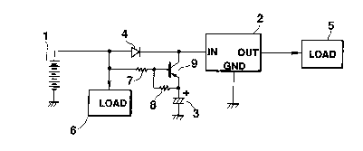
FIG. 2 is a circuit diagram indicative of one
embodiment of a power supply backup circuit according to

the present invention. In FIGs. 1 and 2, the same


Z0~2360
-- 5
reference numeral is used to denote the same element.
As shown in FIG. 2, a PNP transistor 9 is
provided the collector of which is connected to the
junction point of a reverse current preventing diode 4 and
a voltage regulator 2, and the emitter of which is
connected to a non-grounding terminal of a capacitor 3.
The base of the transistor 9 is connected via a resistor 7
to the anode of the diode 4 and via a resistor 8 to the
non-grounding terminal of the capacitor 3.
Therefore, the PNP transistor 9 is positioned
between the non-grounding terminal of the capacitor 3 and
the junction point of the diode 4 and regulator 2 and
functions as a first current path without a current
limitter and allowing a discharge current to blow from the
capacity 3.
The resistors 7 and 8 are positioned between the
anode of the diode 4 and the non-grounding terminal of
the capacitor 3 to function as second current path
including a current limitter.
In operation, if the DC power source 1 is
normal, the load 6 is fed directly from the power source 1
while the load 5 is fed via the diode 4 and voltage
regulator 2. At this time, the transistor 9 is turned
off, so that the charging current to the capacitor 3 is
limited by the second current path constituted by the
resistors 7 and 8.
If the power source 1 is interrupted, the
transistor 9 is turned on, so that the electric charges


201236~)
-- 6
stored in the capacitor 3 are fed via the first current
path including the transistor 9 to the load 5 without
being limited at all.
Since the current flowing to the load 6 is
limited by the resistors 7 and 8 constituting the second
electric path, no useless current is fed to the load 6.
According to the particular embodiment, the
charging current flowing through the capacitor 3 is
limited by the resistors 7 and 8 constituting the second
path, so that the capacitor 3 will not be broken, etc.,
due to rapid charging even if the capacitor 3 includes a
tantalum electrolytic capacitor suitable for high density
integration.
If the DC power source 1 is interrupted and the
capacitor 3 discharges, the transistor 9 constituting the
first electric circuit is switched to a complete
conductive state and the very charged voltage across the
capacitor 3 is applied to the input of the voltage
regulator 2. As a result, enough voltage is supplied to
the load 5.
When the transistor 9 is on, the load 5 is
connected to the capacitor 3 to thereby prevent rapid
discharging.
FIG. 3 is a circuit diagram of another
embodiment of the power supply backup circuit according to
the present invention. In FIGs. 2 and 3, the same element
is given the same reference numeral and further
description thereof will be omitted.


201236~

The feature of the particular embodiment is
characterized by a second electric current path including
a resistor 10 additionally provided between the non-
grounding terminal of the capacitor 3 and the junction
point of the diode 4 and regulator 2.
According to the particular embodiment, the rate
of charging the capacitor 3 is increased while limiting
useless discharge from the capacitor 3 to the load 6.
As described above, according to the embodiments
of FIGs. 2 and 3, no useless voltage drop will occur
during discharging while the charging current to the
capacitor 3 is limited. Thus, if the capacitor 3 includes
a tantalum electrolytic capacitor suitable for high
density integration, its deterioration and breakage are
prevented and enough voltage is supplied to the load.
While in the above embodiments the resistors 7,
8 and 10 and the transistor 9 are used to form the first
and second current paths, respectively, the transistor is
not necessarily required.


Representative Drawing
A single figure which represents the drawing illustrating the invention.
Administrative Status

For a clearer understanding of the status of the application/patent presented on this page, the site Disclaimer , as well as the definitions for Patent , Administrative Status , Maintenance Fee  and Payment History  should be consulted.

Administrative Status

Title Date
Forecasted Issue Date 1995-08-01
(22) Filed 1990-03-16
Examination Requested 1990-03-16
(41) Open to Public Inspection 1990-09-16
(45) Issued 1995-08-01
Deemed Expired 2001-03-16

Abandonment History

There is no abandonment history.

Payment History

Fee Type Anniversary Year Due Date Amount Paid Paid Date
Application Fee $0.00 1990-03-16
Registration of a document - section 124 $0.00 1990-09-19
Maintenance Fee - Application - New Act 2 1992-03-16 $100.00 1991-12-19
Maintenance Fee - Application - New Act 3 1993-03-16 $100.00 1993-01-06
Maintenance Fee - Application - New Act 4 1994-03-16 $100.00 1994-02-03
Maintenance Fee - Application - New Act 5 1995-03-16 $150.00 1995-01-30
Maintenance Fee - Patent - New Act 6 1996-03-18 $150.00 1996-01-08
Maintenance Fee - Patent - New Act 7 1997-03-17 $150.00 1997-02-17
Maintenance Fee - Patent - New Act 8 1998-03-16 $150.00 1998-02-19
Maintenance Fee - Patent - New Act 9 1999-03-16 $150.00 1999-02-17
Owners on Record

Note: Records showing the ownership history in alphabetical order.

Current Owners on Record
KABUSHIKI KAISHA TOSHIBA
Past Owners on Record
ISHII, TAKAAKI
SAKANISHI, MASAYUKI
Past Owners that do not appear in the "Owners on Record" listing will appear in other documentation within the application.
Documents

To view selected files, please enter reCAPTCHA code :


To view images, click a link in the Document Description column. To download the documents, select one or more checkboxes in the first column and then click the "Download Selected in PDF format (Zip Archive)" or the "Download Selected as Single PDF" button.

List of published and non-published patent-specific documents on the CPD .

If you have any difficulty accessing content, you can call the Client Service Centre at 1-866-997-1936 or send them an e-mail at CIPO Client Service Centre.


Document
Description 
Date
(yyyy-mm-dd) 
Number of pages   Size of Image (KB) 
Cover Page 1995-08-01 1 17
Abstract 1995-08-01 1 22
Representative Drawing 1999-07-27 1 3
Abstract 1995-08-01 1 22
Description 1995-08-01 7 236
Claims 1995-08-01 4 113
Drawings 1995-08-01 1 12
Office Letter 1990-10-01 1 20
PCT Correspondence 1995-05-23 1 29
Fees 1997-02-17 1 73
Fees 1996-01-08 1 54
Fees 1995-01-30 1 52
Fees 1994-02-03 1 50
Fees 1993-01-06 1 34
Fees 1991-12-19 1 20