Note: Descriptions are shown in the official language in which they were submitted.
2i~
- PRII~Z, LEISER, BUNKE & PARTNER
Patentanwalte European Patent Attorn~ys
Me~ i"gervveg 7 8000 Munchen ôO
German Patent Application P 39 12 016.3
filed on April 12, 1989
TEXAS INSTRUMENTS DEUTSCHLAND GMBH
Our Fils: T 4907 DE
Damping circuit for the antenna resonance circuit of a
radio transmitter-receiver
The invention relates to a damping circuit for the antenna
resonance circuit of a radio transmitter-receiver which in
a transmitting phase transmits a time-limited energy-rich
HF interrogation pulse and in a receiving phase following
the transmitting phase is ready to receive high-frequency
response signals coming from a responder which transmits
said response signals as a reaction to the reception of the
interrogation pulse.
GB-A-2,077,555 discloses a transponder system in which a
radio transmitter-receiver acting as interrogator cooperates
with one or more responders. The cooperation is carried out
in that the radio transmitter-receiver transmits a high-
energy HF interrogation pulse which is received by a respon-
der located within the range of the transmitting antenna,
said responder thereby being activated to send back a signal
which contains a code clearly identifying the transmitting
responder. How the code is formed in detail is of no conse-
quence in the present case. The peculiarity of the respon-
der resides in that it does not contain its own energy source
~ .. . .
.
.
2 ~ ~. h~
1 but draws its energy from the received HF interrogationpulse by rectification and storing. To enable the radio
transmitter-receiver to transmit an HF interrogation pulse
containing as much energy as possible the antenna resonance
circuit must be as far as possible a resonance circuit with
high quality which then also has a correspondingly narrow
band. Since as mentioned the responder does not contain
its own energy source but draws its energy from the received
HF interrogation pulse, the sending back of the response
signal must take place as quickly as possible because for
this responding operation relatively little energy is avail-
able. To enable a large number of different responders to
be distinguished by their own code a predetermined number
of data bits is necessary for the code and these must be
sent back to the radio transmitter-receiver. The higher
the number of data bits the higher the repetition frequency
of the individual data bits. This high repetition frequency
requires however on the receiver side of the radio
transmitter-receiver an antenna resonance circuit with as
broad a band as possible. In the known transponder system
these contradictory requirements of the antenna resonance
circuit are overcome in that a separate antenna is employed
for the transmission and a separate antenna for the reception
each having corresponding antenna resonance circuits. How-
ever, in order to simplify the radio transmitter-receiver
it would be desirable to use one and the same antenna with
a single antenna resonance circuit for transmission and for
reception.
The invention is based on the problem of providing a damp-
ing circuit for the antenna resonance circuit of a radio
transmitter-receiver which makes it possible to use a single
antenna for the transmission of a high-energy HF pulse and
the reception of HF signals.
1 According to the invention this problem is solved by a damp-
ing member adapted to be connected to the antenna resonance
circuit and separated therefrom, a switching means which on
reception of a switching voltage connects the damping member
to the antenna resonance circuit, a first energy-storage
element chargeable by the HF interrogation pulse for furnish-
ing the switching voltage and a second energy-storage ele-
ment which is chargeable by the HF interrogation pulse and
which in dependence upon the time profile of the HF interro-
gation pulse enables the application of the switching volt-
age present at the first energy-storage element to the
switching means.
The damping circuit according to the invention permits switch-
over of the quality of the antenna resonance circuit, said
switchover taking place automatically in dependence upon the
profile of the HF interrogation pulse in the sense that the
antenna resonance circuit has the necessary high quality
during the presence of the HF interrogation pulse so that
accordingly a high-energy HF interrogation pulse can also be
transmitted whilst on termination of said pulse switchover
to a low quality takes place automatically by connecting
the damping member to the antenna resonance circuit so that
the wide band of the antenna resonance circuit necessary for
reception is achieved. This switchover has a further ad-
vantageous effect due to the fact that the radio transmitter-
receiver after termination of the HF interrogation pulse
moves very rapidly into the ready-to-receive state because
due to the connection of the damping member the decay of
the oscillation of the antenna resonance circuit takes place
at high speed so that the reception of an HF siqnal possibly
transmitted by a responder is possible immediately after
termination of the HF interrogation pulse. This is a par-
ticularly great advantage when the responder does not con-
tain its own energy source but must operate with the energy
2 ~ 3~ ~
1 drawn from the HF interrogation pulse and stored in a capa-
citor. Since the storing of this energy is of course
limited the responder must send its HF signal back as quickly
as possible after termination of the HF interrogation pulse
in order to make optimum use of the stored energy.
Advantageous further developments of the invention are
characterized in the subsidiary claims:
The invention will now be explained by way of example with
the aid of the drawings, wherein:
Fig. 1 is a fundamental diagram of a radio transmitter-
receiver which cooperates with responders and in
which the damping or attenuation circuit according
to the invention is used, and
Fig. 2 is a circuit diagram of the antenna resonance cir-
cuit with the damping circuit according to the
invention.
The transponder system illustrated in Figure 1 includes a
radio transmitter-receiver 10 at the front side of which a
rod-like antenna 12 is disposed. The radio transmitter-
receiver 10 comprises a grip 14 on which an activating
switch 16 is disposed. On each actuation of the activating
switch 16 a transmitter section is activated and as a result
a high-energy ~F interrogation pulse is transmitted by means
of the antenna 12. As indicated schematically, in the tip
18 of the antenna 12 a ferrite rod 20 is incorporated which
is surrounded by an antenna winding 22. Furthermore, a
damping circuit 24 indicated schematically in Figure 1 is
accommodated in the antenna 12.
The radio transmitter-receiver 10 illustrated in Figure 1
cooperates with a responder 26 which is shown only
i
.
.
~' '
..
2 ~
-
s
1 schematically. Said responder may be attached to an object
to be identified or built into an object to be identified.
For example, the responder 26 could also be attached to
the earmark of a cow making it possible to identify the cow
by interrogation of the responder attached thereto. The
responder could also if necessary be implanted in the skin
of an animal. Although in Figure 1 only one responder 26
is shown in a real application case a great number of re-
sponders may be present which can each be interrogated in
that the antenna 12 of the radio transmitter-receiver 10 is
moved into the vicinity of the respective responder 26 and
the interrogation pulse is transmitted by actuating the ac-
tivating switch 16.
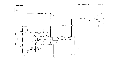
In Figure 2 the electrical circuit diagram of the antenna
resonance circuit 28 and the damping circuit 24 connected
thereto are illustrated. The antenna resonance circuit 28
is coupled by means of a winding Wl to a winding, not illu-
strated, in the transmitter-receiver 10. The winding W3
of the antenna resonance circuit 28 is wound round the
ferrite rod 20. The winding Wl, the winding W3 and two
capacitors CAl and CA2 are connected in series in the antenna
resonance circuit 28.
The damping circuit 24 comprises two inputs El and E2 to
which a winding W2 is connected which like the winding Wl is
coupled to a winding in the radio transmitter-receiver 10.
Connected to the input El is the anode of a diode Dl, the
cathode of which is connected to the collector of a transis-
tor Tl. Between the collector of the transistor Tl and its
base there is a resistor Rl. The cathode of the diode Dl
is also connected to a capacitor Cl which is connected at
the input E2. The potential present at the input E2 is
taken as ground potential in the damping circuit 24. The
line 30 connected to the input E2 is therefore referred to
as ground line.
,
~ . ,
~ '
J ~
1 The base of the transistor Tl is connected to the collector
of a transistor T3 of which the base is connected via a
resistor R2 to the ground line 30. Furthermore, to the base
of the transistor Tl the cathode of a Zener diode DZ is
connected, the anode of which is connected to the ground
line 30. The emitter of the transistor Tl is connected to
the anode of a further diode D3 the cathode of which is
connected to the emitter of a transistor T2 of which the
collector is connected to the ground line 30. The base of
the transistor T2 is in connection with the base of the
transistor Tl and with the collector of the transistor T3.
Furthermore, the cathode of the diode D3 leads to the gate
electrodes of two field-effect transistors T4 and T5 which
are MOS field-effect transistors of the enhancement type.
The drain electrode of the field-effect transistor T4 is
connected to the connecting line between the winding Wl and
the capacitor CAl of the antenna resonance circuit 28 whilst
its source electrode is connected to the ground line 30.
The drain electrode of the field-effect transistor T5 is
connected via a series circuit of three resistors R4, R5 and
R6 to the connecting point of the two capacitors CAl and
CA2; it source electrode is connected to the ground line
30. Also connected to the input El is the cathode of a
diode D2 of which the anode is connected viaa capacitor C2 ~o the
ground line 3U and via a parallel clrcui, of a capacitor CJ dnd a res1stor
R3 to the emitter of the transistor T3. ~he series circuit of the three~
sistors can of course be replaced by a single resistor.
The damping circuit of which the construction has been
described operates as follows:
If all the capacitors in the damping circuit 24 are dis-
charged and the transmitter section of the radio transmitter-
receiver 10 is deactivated, the damping circuit 24 is not
active. In this state the series circuit of the resistors
.
'
';
" , , '
:' ' ' , ~ '
'~ ' ' ,
,
,
J ~
.
1 R4, R5 and R6 acting as damping member is not connected in
parallel to the capacitor CAl and consequently the antenna
resonance circuit is not damped by said damping member. The
antenna resonance circuit therefore has a high circuit
quality so that on corresponding energy supply to the wind-
ing W1 by means of the winding W3 it can generate a strong
magnetic field with small harmonic content.
When the activing switch 16 is actuated an AC voltage is in-
duced in the winding W2 and is applied via the inputs E1
and E2 to the damping circuit 24. Due to the effect of the
diode D1 the voltage at the input El generates a positive
voltage at the capacitor Cl whilst the diode D2 generates a
negative voltage at the capacitor C2. At the start of the
HF interrogation pulse at the capacitor C2 a voltage jump
occurs and as a result via the capacitor C3 a negative po-
tential is applied to the emitter of the transistor T3 so
that the collector of the transistor T3 takes on the current
flowing through the resistor Rl. At the same time, a volt-
age lying close to ground potential is thereby applied tothe base of the transistor T2 so that the emitter of the
transistor T2 keeps the gate electrodes of the two field-
effect transistors T4 and TS with low resistance almost at
ground potential. This low-resistance state of the field-
effect transistors T4 and T5 prevents said enhancement field-
effect transistors rendering themselves conductive due to
the high AC voltage at their drain terminals via their drain/
gate capacitances, thus leading to a damping of the antenna
resonance circuit by connection of the resistors R4, R5, R6
in parallel with the capacitor CAl.
During the reception of the HF interrogation pulse the Zener
diode DZ is forward conducting and together with the resis-
tor R2 prevents excessive saturation of the transistor T3.
Excessive saturation of said transistor T3 is to be avoided
-
1 because said transistor after termination of the HF inter-
rogation pulse must react as quickly as possible and this
could not be achieved with excessive saturation. Moreover,
the Zener diode DZ prevents the voltage exceeding or dropp-
ing below the maximum admissible gate voltage at the field-
effect transistors T4 and T5.
The diode D3 ensures that the transistor Tl is not conduct-
ive during the reception of the HF interrogation pulse.
After the capacitor C3 has been charged to its end voltage
the resistor R3 furnishes enough current to the emitter of
the transistor T3 to prevent the damping action from occurr-
ing because the transistor Tl remains nonconductive.
As soon as the capacitor Cl has been charged to its end volt-
age the requirements are present for a rapid damping of the
antenna resonance circuit and the resultant switchover of
the quality from a high value to a low value after termin-
ation of the HF interrogation pulse.
Although as soon as the HF interrogation pulse ends the volt-
age in the antenna resonance circuit rises for a few more
periods, the resonance circuit current then drops due to
the inherent damping of the antenna resonance circuit so that
the negative charge voltage at the capacitor C2 also begins
to drop. This manifests itself via the capacitor C3 as
positive voltage jump at the emitter of the transistor T3.
The capacitors Cl and C2 and the resistors Rl and R3 are so
dimensioned that the time constant Cl/R1 is greater than
the time constant C2/R3. As a result, in contrast to the
voltage at the capacitor C2 the voltage at the capacitor Cl
remains substantially constant over the period of time con-
sidered. Due to the already described positive voltage jump
. ~, .
~. s
J ~ 2
l at the emitter of the transistor T3 the transistor Tl becomesconductive. At its emitter the voltage therefore rises and
passes via the diode D3 to the gate electrodes of the field-
effect transistors T4 and T5. As soon as the threshold
voltage of these field-effect transistors T4, T5 is exceeded
the damping member formed from the series circuit of the
resistors R4, R5 and R6 connects itself in parallel with
the capacitor CAl which is a partial capacitance of the
antenna resonance circuit 28.
The damping member could however also be connected to the
antenna resonance circuit via an inductive tap, connection
to the entire antenna resonance circuit would also be poss-
ible. The reason for connecting the damping member in via
an inductive or also capacitive tap is that at the maximum
resonance circuit voltage occurring the maximum admissible
drain/gate voltage of the field-effect transistor T4, T5
must not be exceeded. Moreover, the connecting of the damp-
ing member in at such a tap can be expedient if the damping
resistance together with the parasitic capacitances, in par-
ticular taking account of the not inconsiderable capacitances
of the nonconductive field-effect transistors T4 and T5, form
an RC member having a limit frequency in the vicinity of or
beneath the operating frequency of the overall system.
The charging or recharging of the capacitances of the field-
effect transistors T4 and T5 withdraws from the capacitor Cl,
serving as energy store, a considerable proportion of its
energy. The greatest part of the energy is used by the
drain/gate capacitance and the high AC voltage during the
switching-on phase of the field-effect transistors T4, T5.
Thereafter, account need only be taken of leakage currents
in the circuit so that with components having small leak-
age currents the damping phase in which the damping member
comprising the resistors R4, RS and R6 is active can be
several times the necessary receiving time.
2 ~ ~ 2 J'V~
1 Inherent to the design, the field-effect transistors T4 and
T5 comprise internally between the drain electrode and the
source electrode an "inverse diode" and as a result for
operation with AC voltage two field-effect transistors are
required for the disconnection, of which depending on the
polarity of the voltage one is always conductive via its
internal diode. For the winding W2 this means that it is
applied in time with the AC voltage via one of said "in-
verse diodes" alternately to the circuit points 32 and 34
of the resonance circuit. Consequently, the winding W2 must
be well insulated with respect to the winding Wl to avoid
breakdowns occurring at the peak values of the resonance
circuit voltage.
As soon as a new HF interrogation pulse is transmitted due
to the function cycle described above the damping member
comprising the resistors R4, R5 and R6 is again separated
from the antenna resonance circuit 28 so that the antenna
resonance circuit 28 can again emit the magnetic field with
high circuit quality as is necessary for the response of a
responder 26.
The antenna damping circuit described thus operates com-
pletely automatically in dependence upon the occurrence of
an HF interrogation pulse; it does not require its own
current supply source but derives the energy necessary for
its operation from the HF interrogation pulse. The damping
of the antenna resonance circuit 28 achieved after completion
of the HF interrogation pulse by employing the damping cir-
cuit 24 not on~y effects the changeover of the quality ofthe antenna resonance circuit 28 but also makes said circuit
and thus the radio transmitter-receiver 10 ready-to-receive
the signals returned by the responder 26 immediately after
termination of the HF interrogation pulse.