Note: Descriptions are shown in the official language in which they were submitted.
2 ZO1;3(JZ9
FIELD-BASED MOVEMENT SENSOR
This invention relates in general to apparatus for
sensing movement, and in particular instances to devices
for measuring strain in an object and devices for
measuring acceleration.
Measurement of strain (the change in length of an
object in some direction per unit undistorted length) in
specimens and objects may be carried out either directly
or indirectly. Some of the approaches used for direct
strain measurements include the use of bonded wire strain
gages ~in which a grid of strain-sensitive wire is
cemented to a specimen so that a change in the length of
the grid due to strains in that specimen changes the
resistance of the wire which can then be measured),
mechanical strain gages (in which optical or mechanical
lever systems are employed to multiply the strain which
may then be read from a suitable scale), magnetic strain
gages (which include magnetic circuits having air gaps
which, when varied as a result of a strain in the
specimens, varies the permeance o the circuits to
provide an indication of the strains produced),
semiconductor strain gages (in which the resistance of a
piezoresistive material varies with applied stress and
resulting strain in the material~, and capacitance strain
gages (in which a variation of capacitance caused by
variation in the separation of elements due to strain in
the specimen, can be measured to provide a reading of the
strain). Other direct strain measuring devices include
acoustic strain gages, brittle lacquer coa~ings, photo
grids and cathetometers.
2~
Approaches for indirectly measuring strain in a
specimen include the use of displacement pickup devices,
velocity pic~up devices and acceleration detection
devices.
A disadvantage of the conventional approaches to
measuring strain (or forces including those produced by
acceleration, weight, or the like), is that the devices
employed are oftentimes difficult to attach to or to use
with a specimen whose strain is to be measured. Also,
such devices are typically difficult and costly to
manufacture. Finally, because of the intrinsically high
axial rigidity of many of such devices, it requires high
quality bonding of the device to the specimen to prevent
detachment due to failure of the bond and this, in turn,
rec~uires time-consuming and care~Eul preparation of the
specimen for bonding.
One approach to measuring forces in general has
included the use of a parallelogram-type structure in
which are mounted capacitive elements arranged to measure
forces applied to the structures. Examples of some such
devices include those disclosed in U.S. Patent Nos.
4,092,856, 4,308,929, 4,572,006 and 4,649,759. All but
one of the devices disclosed in these patents utilize
variation of capacitance resulting from variation in the
separation of the capacitive elements as the mechanism
for measuring force. The capacitive elements are mounted
on the structures in face-to-face relationships and so
the structures are typically fairly bulky, having non-
planar profiles. Such structures would be difficult to
adapt for use as strain gages since, because of their
bulk and size, it would be difficult to attach the
structure to specimens or objects in which strain is to
be measured. Also, fabricating the structures with the
capacitive elements in the face-to-face relationship is
quite difficult since multiple surfaces or faces of the
structure must be prepared and treated.
It is an object of the invention to provide a
Zt~3(~2~
movement sensor which is easy to fabricate, simple in
design and readily usable for measuring a variety of
forces and movement imposed generall~ along an axis.
It is also an object of the invention to provide such
a sensor which has a relatively low, flat profile
suitable for attaching to an object in which strain is to
be measured.
It is a further object of the invention to provide
such a sensor which is relatively small in size and well-
suited for use with semiconductors and integratedcircuits.
It is an additional object of the invention to
provide such a sensor which can be fabricated utilizing
conventional integrated circuit fabrication technology.
It is also an object of the invention to provide such
a sensor in which a single surface mounting of force or
movement measuring elements is possible.
The above and other objects of the invention are
reali~ed in one specific illustrative embodiment of a
movement sensor adapted for measuring movement or strain
along a certain axis in an object to which the sensor is
attached. The sensor includes a substrate having a
working surface and formed with a pair of fingers
projecting from a first direction, and a third finger
projecting from a direction opposite the first direction
to a position between the pair of fingers. The pair of
fingers and third finger extend generally perpendicular
to the axis along which strain is to be measured, with
the pair of fingers being movable with respect to the
third finger along the axis when the strain occurs in the
object. A force field producing element, such as an
electrically charged element or a magnetic field-
producing element, is disposed on the working surface of
the third finger, and a pair of force field detecting
elements/ such as a field-effect transistor capable of
detecting electric fields or split drain magnetic field-
effect transistors capable of detecting magnetic fields,
13l~2~
are each disposed on a working surface of a different one
of the pair of fin~ers. As the object on which the
substrate is attached is subjected to strain causing the
pair of fingers to move relative to the third finger, the
variations in the s~rength of the force field from the
force field producing element to the force field
detecting elements is determined and this provides a
measure of -the variation in distance between the third
finger and the pair of fingers. The variation in
distance between the fingers, in turn, provides a measure
of the strain in the object to which the substrate is
attached.
DESCRIPTIO~ OF THE DRAWI~GS
The above and other obiects, features and advantages
of the invention will become apparent from a
consideration of the following detailed description
presented in connection with the accompanying drawings in
which:
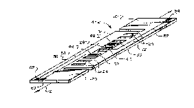
FIG. 1 is a perspective view of a flexible uniaxial
strain transducer made in accordance with the principles
of the present invention;
FIGS. 2A and 2B show top plan views of the transducer
of FIG. 1 when under tensile strains and compressive
strains respectively,
FIG. 3 is a schematic of an exemplary circuit which
may be utilized for producing a signal indicative of the
strain to which the FIG. 1 transducer is subjected;
FIG. 4 shows a top plan, fragmented view of a strain
transducer which includes a plurality of sensor
combinations;
FIG. 5A shows a top, plan view of another embodiment
of a strain transducer made in accordance with the
principles of the present invention and which utilizes
~he Vernier principle of measurement;
FIGS. 5B, 5C and 5D show graphic representations of
the use of the strain transducer of Fig. 5A;
FIG. 6 shows a top, plan view of another embodiment
~Q~3~i29
of a strain transducer made in accordance with the
principles of the present invention and which also
utili~es the Vernier principle.
FIG. 7 shows a top, plan view of an acceleration
force transducer made in accordance with the principles
of the present invention;
FIG. 8 shows a top plan view of an embodiment of a
force transducer made in accordance with the principles
of the present invention in which magnitude but not
directional force can be determined;
FIG. 9 shows a top plan view of a uniaxial force
transducer in which magnitude and two direction of force
can be determined;
FIG. 10 shows the top, plan view of a biaxial force
transducer in which magnitude and four directions of
force can be determined;
FIGS. llA, llB and llC show graphic top, plan view
representations of three embodiments of rosette strain
transducers made in accordance with the principles of the
present invention; and
FIG. 12 shows a top, plan view of a strain transducer
with mechanical amplification.
Referring now to the Drawings:
Referring to FIG. 1 there is shown one illustrative
embodiment of a flexible uniaxial strain transducer for
measuring the strain in an object to which or on which
the transducer is attached. The transducer includes a
generally planar, low-profile silicon substrate frame
member 4 having a top working surface on which working
parts of the transducer are disposed, and a bottom
surface. The frame member 4 includes a pair of generally
parallel load-bearing beams or side rails 8 and 12 which
are movable longitudinally with respect to one another
when the object on which the transducer is attached is
subject to strain. Formed on respective ends of the
beams 8 and 12, at opposite ends, are bonding pads 16 and
20. The bonding pads are generally co-planar with the
Z~
beams 8 and 12 and extend ~rom the respective beam on
which they a~e formed to a location adjacent to and
spaced from the end of the other beam. The bonding pads
16 and 20 allow for attaching the transducer by a
suitable adhesive to the object in which the strain is to
be measured. A plurality of laterally flexible
connecting beams or struts 24 extend between and connect
the beams 8 and 12. The struts 24 are generally
perpendicular to the beams 8 and 12, as shown in FIG. 1.
A first projection 28 extends from beam 12 toward beam 8
to a location between a second projection 32 and a third
projection 36, both of which extend from beam 8 toward
beam 12.
Disposed on and formed, for example, by conventional
microfabrication techniques on the working surface of
projection 28 is an emitter 40 for developing an electric
field. The emitter, for example, might illustratively be
a charged electric conductor. Disposed on and formed,
for example, also by conventional microfabrication
techniques such as vacuum deposition on the working
surfaces of projections 32 and 36 are two detectors
which, in this embodiment, are field-effect transistors
(FETS) 44 and 48 respectively. A conductor 52 connects
the conductive emitter 40 to an edge electrical contact
pad 54 for connecting to an electrical charge source and
conductors 56 and 58 connect respectively FET 44 and FET
48 to edge electrical contact pads 60 and 62 for
connecting to sensor circuitry such as that shown in
FIG. 3.
The emitter 40 might alternatively be a layer of
material containing positive or negative charges. For
example, the emitter could illustratively be a layer of
polytetrafluoroethylene with electrons implanted therein.
The FETS 44 and 48 include conductive gates which are
influenced by the electric field produced by the
conductive emitter 40, with the degree of influence being
determined by the spacing between the projection 28 and
Z~3(}~
res~ctive projections 32 and 36, i.e., the separation
between the source of the electric field and the
conductive gates of the FETS. The operation of FETS is
well-known as is the effect of an electric field on the
conductive gate of an FET. The FET includes two
conductive regions, known as the drain and source
regions, separated by a channel region which is
conductive. The drain region and source region are
maintained at different electrical potentials so that
electric current is caused to flow between the regions
through the channel. The gate of an FET is positioned
adjacent the channel region and when the FET is exposed
to an electric field, an electrical charge is induced on
the surface of the gate to affect the conductivity of the
channel region. This in turn determines the magnitude of
the electrical current which flows between the drain
region and the source region. While measuring this
electrical current flow, a determination can be made as
to the proximity of the source of an electric field
positioned near the FETS. A further discussion of this
pnenomenon is found in U.S. Patent No. 4,767,973, issued
August 30, 1988, which is incorporated herein by
reference.
Although the FIG. 1 embodiment is shown using a
conductive emitter 40 and FETS 44 and 48, it should be
understood that alternatively, the conductive emitter 40
could be replaced with a magnetic field emitter such as a
permanent magnet or an electromagnet and the FETS could
be replaced with split drain magnetic FETS (MAGFETS)
capable of detecting magnetic fields. Then, the MAGFETS
would detect the spacing between each of the MAGFETS and
the permanent magnet located on projection 28.
Briefly, a MAGFET is a metal-oxide semiconductor
field-effect transistor (MOSFET) with ~wo drains, i.e.,
the MAGFET has a source region, two drain regions, a
conductive channel region between the source region and
two drain regions, and a gate located adjacent to the
:~Q~
channel region. In the absence of a magnetic field,
current flows from the source region through the channel
region equally to the two drain regions. When a magnetic
field is present, the current through the channel region
is deflected to flow more ~o one drain region than the
other, with the magnitude of the deflection and thus
imbalance of current flowing to the two drain regions
being dependent upon the intensity of the magnetic field.
Measuring the current imba]ance in the two drain regions
thus provides a measure of the proximity of a magnetic
field source to the MAGFET.
The FIG. 1 embodiment shows the use of two detectors
(FETS 44 and 48) positioned on either side of one emitter
40 and the advantage of this two-detector arrangement
will be made clear momentarily. However, it should be
recognized that use of a single detector disposed on one
projection, positioned on one side of the emitter 40,
could also serve to detect strain, i.e., movement of
bonding pad 16 relative to bonding pad 20, as will be
discussed in connection with FIGS. 2~ and 2B.
FIGS. 2A and 2B show, in an exaggerated fashion, the
effect on the transducer 4 of a stress (pullin~ apart)
and a compressive force (squeezing to~ether)
respectively. In FIG. 2A, the affect of a stress on the
object on which the transducer 4 is disposed is that
bonding pads 16 and 20 are pulled apart and projection 28
thus moves away from projection 32 and toward projection
36 as shown. The FET deposited on projection 36 thus
detects the increase in strength of the electric field
being produced by the conductive emitter on projection 28
and thus the magnitude of movement of the projection 28
toward the projection 36, whereas the FET on projection
32 detects the decrease in the strength of the electric
field and thus the magnitude of the movement of the
projection 28 away from the projection 32. The
difference be~ween the increase in the s~rength of the
electric field and the decrease in the strength of the
3(~2~
electric field may be determined by a differential
circuit shown in FIG. 3 to produce a resultant signal
which more accurately indicates the magnitude of
movement of the beams 8 and 12 relative to one another to
thereby accurately measure the strain developed in the
object on which the transducer 4 is mounted.
FIG. 2B shows, in exaggerated form, the affect of a
compressive force applied to the transducer 4 in which
case projection 28 is moved closer to projection 32 and
farther away from projection 36. Again, the distance of
this movement can be measured by the FETS located on
projections 32 and 36 as earlier described.
Although the substrate frame 4 was described as being
made of silicon, it could also be made of other materials
such as polysilicon, sapphire, amorphous silicon,
germanium, gallium arsenide, etc. Also, although the
entire FETS were described as being deposited on
projections 3~ and 36, it may be desirable to simply
deposit the gages of the FETS on those projections and
deposit the remaining parts of the FETS remotely from the
gates either on the frame 4 or at some other location.
In such case, the gates on the projections 32 and 36
would be coupled by appropriate conductors to the
respective FETS of which they would be a part.
FIG. 3 is a schematic of one illustrative
differential circuit which could be ùtilized with the
transducer of FIG. 1 to measure movement of the
projections 32 and 36 relative to the projection 28 and
thus strain in an object on which the transducer is
mounted. The circuit includes a charge source or
voltage source 57 coupled to the emitter 40 on projection
28, a voltage source 59 coupled to the drain regions of
the FETS 44 and 48, two current-to-voltage converters 61
and 63, each coupled to a respective source region of the
FETS 44 and 48, and two voltage amplifiers 65 and 67.
The polarities of the voltage signals produced by the
amplifiers 65 and 67 are opposite, and these signals are
supplied to a comparator 69 which produces an output
signai whose amplitude is proportional to the difference
in magnitude of the input signals (indicating the
magnitude of movement of the projections 32 and 36
relative ~o projection 28), and whose polarity is
determined by the direction of movement of the
projections. In this manner, both the magnitude of the
strain in the object being measured and whether the
strain is tensile or compressive can be determined.
FIG. 4 shows a fragmented transducer having multiple
sets 70 of two projections containing detection elements
and one projection situated between the two projections,
containing a force field producing element. By providing
multiple sets of such force field producing elements and
detection elements, the signal outputs can be su~ned to
provide a better signal-to-noise ratio for the
transducer. A sumnling amplifier 72 is shown coupled to
the outputs of two comparators 74 and 78.
FIG. 5A shows a top, plan view of another embodiment
of a strain transducer constructed of two pieces, both of
which would be applied to the o~ject in which strain was
to be measured. The transducer of ~IG. 5A includes a
pair of load-bearing, spaced-apart generally parallel
rails 80 and 84. A bonding pad 88 is joined to one end
of the rail 80 to extend toward an end of the rail 84,
and a bonding pad 92 extends from the other end of the
rail 84 toward an end of the rail 88 as shown. The
bonding pads 88 and 92 are provided for attaching the
transducer to an object in which strain is to be
measured.
Also included are a pair of arms 96 and 100 extending
respectively from rails 84 and 80 to positions generally
parallel with and side-by-side with one another. Arm 96
is positioned between arm 100 and rail 80, whereas arm
100 is positioned between arm 96 and rail 84. A
plurality of force field emitters 104 are spaced apart
longitudinally along arm g6 in a multiplicity (one less
?(~3Q~g
12
than tl~e number of force field emitters) of force field
detector elements are spaced apart longitudinally alon~
arm 100. As can be seen, the endmost force field
emitters of ~he array are positioned opposite respective
endmost lines of the force field detector elements, when
the transducer is not being subjected to a stress or a
compressive force. FIG. 5B better illustrates the
positions of the force field emitters 104 relative to the
force field detector elernents 108 when the transducer is
in the no or zero strain condition. The configuration of
force field emitters 104 relative to the force field
detector elements 108 is similar to a Vernier scale
arrangement. That is, a small movement of the arms 96
and 100 relative to one another to increase the
sensitivity of the transducer to strains occurring in the
object on which the transducer is mounted.
FIG. SC illustrates relative movement of the arms 96
and 100 when a compressive force is applied to the
transducer. In this case, the endmost force field
emitters become misaligned with the endmost force field
detector elements and the second from the right force
field emitter 104a comes into alignment with the second
from the right force field detector element 108a as
shown. When this happens, the force field detector
element 108a detects the close proximity of the force
field emitter 104a to provide a readout indicating the
magnitude of relative movement of the arms. Continued
relative movement of the arms 96 and 100 as shown in
FIG. 5G will ultimately bring into alignment the third
from the right force field emitter and force field
detector element, etc., to progressively provide a
readout of the movement of the arms.
FIG. 5D shows relative movement of the arms 96 and
100 when the transducer is subjected to a stress so that
the second from the left force field emitter 104b comes
into alignment with the second from the left force field
detector element 108bA With this alignment and close
3~2~
13
proximity, a readout of the ~orce field detector element
108b would provide an indication of the magnitude of
relative movement of the arms. Similarly, as the arms 96
and 100 continue relative movement as indicated in FIG.
5D, then the second from the left force field emitter and
force field detector element come into alignment, etc.
FIG. 6 shows a top, plan view of another embodiment
of a strain transducer which utilizes the Vernier
principle. This transducer includes a flexible generally
planar frame member 120 having a pair of load-bearing,
spaced-apart generally parallel rails 124 and 128, a pair
of bonding pads 132 and 136 extending respectively from
respective ends of rails 124 and 128, and a plurality of
spaced-apart laterally flexible connecting struts 140
and 144 extending between and joining the rails 124 and
128. Also included are a pair of co-planar pla~es 148
and 152 which extend respectively from rails 124 and 128
toward one another so that the adjacent free edges 150
and 154 of plates 148 and 152 respectively are generally
parallel with one another. A plurality of force field
emitters 156 are disposed on the upper surface of the
frame member 120 and spaced apart longitudinally along
plate 148 at the free edge 150. Each of the force field
emitters 156 might illustratively comprise an elongate
conductor extending from a common buss 164 (also formed
on the top surface of the frame member 120) to the edge
150 of the plate 148. The common buss 164 is shown in
FIG. 6 connected to a single voltage source 166, but
each of the emitters 156 could be coupled to individual
voltage sources having either different voltage levels or
substantially the same voltage level. Formed on the
other plate 152 are a multiplicity of force field
detector elements which are spaced apart longitudinally
along the plate near the free edge 154. Advantageously,
3~ the force field detector elements 160 comprise elongate
conductors, which serve as gates of FETS and which
extend from a buss 168 deposited cn the top surface of a
;~313~29
14
frame member 120 to the free edge 154 of the plate. The
buss 168, in this case, would contain individual leads or
conductors for each of the conductor strips 160 for
ultimate connection to a different FET. Alternatively,
the ~orce field detector elements 160 could be individual
FETS deposited on the top surface of the frame member 120
so that the gate regions thereof were disposed adjacent
to or at the edge of the free edge 154 of the plate 152.
As with the embodiment of FIGS. 5A through 5D, the
FIG. 6 embodiment is a type of Vernier sca~le arrangement
and movement of the rails 124 and 128 relative to one
another would be detected and determined by which ones of
the force field emitters 156 were in closest proximity to
corresponding ones of the force field detector elements,
in the manner described for the FIGS. 5A through 5D
embodiment.
The FIG. 6 transducer may be readily manufactured
using conventional microfabrication technology to
position the force field emitters 156 and force field
detector elements 160 so that they extend towards one
another to almost touch. Af~er fabrication, the free
edges 150 and 154 could then be cut, for example, by
laser machining, chemical etching, mechanical sawing,
etc., to provide a precise parallel arrangement between
the edges ancl to leave exposed the force field emitters
at edge 150 and the force field detector elements at edge
154.
FIG. 7 shows a top-plan view of an acceleration force
transducer which includes a substrate frame 200. The
frame includes a pair of generally parallel, spaced-apart
rails 204 and 208 and bonding pads 212 and 216 joined to
respective ends of the rail 204. The rail 208 is
connected by laterally flexible cross struts 220 and 224
to the rail 204, as previously described. Fingers 228
and 230 project from rail 204 towards rail 208 to
locations between finger pairs 232 and 236 respectively,
which, in turn, project from rail 208 toward rail 204.
Force field emitters are disposed on fingers 2~8 and 230
and force rield detecting elements are disposed on finger
pairs 232 and 236, all as earlier described for other
embodiments of the invention. Mounted on rail 208 is an
S elongate weight 240 which, when the frame 200 is
accelerated longitudinally either to the right or to the
left FIG. 7, causes rail 208 to move relative to rail 204
in a direction opposite that of the acceleration. This
is indicated by the arrow 244. When rail 208 is caused
to move relative to rail 204, then the pairs of fingers
232 and 236 are caused to move relative to fingers 228
and 230 and this movement is detectable by the force
detector elemen~s deposited on the pairs of fingers 232
and 236. In this manner, the acceleration to which the
frame ~00 is ~eing subjected can be detected and
measured.
FIG. 8 shows a top, plan view of a force transducer
in which the magnitude, but not the direction, of the
force can be determined. This transducer is formed from
a single piece of material to include an annular
substrate 300 on which is disposed an FET 302 having a
source region 303, a gate region 304, and a drain region
305, and a centrally positioned substrate piece 312
supported by integrally formed springs 316. An electric
field emitter 320 is disposed on the substrate piece 312.
The FET 302 is coupled to signal processing circuitry
308.
As the substrate 300 is accelerated in some
direction, the substrate 312 which is suspended by
springs 316 and not attached to the object being
accelerated is caused to move relative to the substrate
300 in a direction opposite the direction of
acceleration. This movement is detected by the FET 302
due to a change in the proximity between the emitter 320
and the gate 304 as previously described. The magnitude
o~ the acceleration of the substrate 300 in any direction
is determined by the proximity of the emitter 320 to the
3(,29
16
gate reqion 304, but the direction of acceleration cannot
be dete~mined by the FIG. 8 transducer.
FIG. 9 shows a top, plan view of an alternative
embodiment of an acceleration force transducer in which
the magnitude of acceleration along one axis 400, in
either direction, can be determined. This transducer
includes a circular substrate 404 with integrally formed
flexible struts 412 and 416 extending inwardly from the
substrate 404. A semicircular FET 420 (having a source
region and drain region positioned on each side of a gate
region) and a semicircular FET 424 are disposed on the
substrate 404, each FET being connected to a respective
one of signal processing circuits 428 and 432. Held in
place in the center of the substrate 404 is an integrally
formed substrate 436 on which is disposed an electric
field emitter 440. As the substrate 404 is accelerated
to the righ, along axis 400, the support struts 412 and
416 flex to the left causing the emitter 440 to move
closer to the gate of FET 420, and this causes both FET
420 and FET 4~4 to produce signals indicating the change
in the proximity of the emitter 440 with respect to the
gates of FETS 420 and 424, as previously described.
Similarly, if the substrate 404 is accelerated to the
left, then the support struts 412 and 416 are caused to
flex to the right moving the emitter 440 into closer
proximity to the gate of FET 424 and farther from the
gate of FET 420. This change in proximity would again be
reflected by the signal outputs of the FETS 420 and 424.
In the manner described, both the magnitude and the
direction along axis 400 of an acceleration force can be
determined.
FIG. 10 shows a top plan view of a biaxial force
transducer in which magnitude and four directions of
acceleration force can be determined. The transducer of
FIG. 10 includes a circular substrate 500, on which are
disposed quarter circle MAGFETS 516, 520, 524 and 528.
Each of these MAGFETS are connected to a respective one
2a~3~
17
of t~le signal processing circuits 532, 536, 540 and 544.
MAG~ET 528 is shown in detail to include a source region
529, gate region 530 and two drain regions 531a and 531b.
Although not shown in ~IG. 10, the other MAGFETS would be
similarly constructed. Suspended in the center of the
substrate 50~ by integrally formed mechanical springs 548
is a substrate 552 on which is disposed a magnetic field
emitter 556. From an examination of FIG. 10, it can be
visualized how acceleration of the substrate 500
generally along either of the axes defined by springs 548
would result in one of the MAGE`ETS producing a signal
indicating closer proximity between that MAGFET and the
emitter 556 and one of the MAGFETS producing a signal
indicating that the emitter 556 has moved away from that
MAGFET. In this manner, the magnitude of acceleration
force in either direction along two different and
orthogonal axes can be determined.
It would be evident that in a manner similar to that
described for the FIGS. 9 and 10 transducers, a
transducer could be provided having a circular substrate
and circular gate region segmented so as to provide
measurements of acceleration force which may occur along
a multiplicity of axes. The measurements would be both
of the magnitude of the acceleration force and the
direction along the particular axis in which the
acceleration occurred.
FIGS. llA, llB and llC show graphic top plan view
representations of a two-element rosette strain
transducer for measuring strains in two orthogonal
directions, a three-element rosette strain transducer and
a four-element rosette strain transducer. In FIG. llA,
the rosette includes a single substrate 600 formed in the
shape of a "T" and cut or etched to accommodate two FET-
or MAGFET-based strain transducers 604 and 608, similar
to the transducer shown in FIG. 1. Transducer 608 is
positioned perpendicularly to transducer 604 as shown.
The substrate 600 is made of a flexible material such as
Z~31)29
18
the substrate materials discussed earlier. Bonding pads
612 and ~16 of transducer 604 and bonding pads 620 and
624 of transducers 608 are provided for attaching the
rosette to the object whose strain is to be measured,
with the long axis of each transducer 604 and 608
positioned to coincide generally with the directions in
which strain is expected in the object. Such strain will
thus be measured by the two transducers 604 and 608.
FIG. llB shows a three-element rosette strain
transducer, with three FET- or MAGFET-based strain
transducers 704, 708 and 712 formed from a single piece
of material and disposed to form an equilateral triangle.
Adjacent ends of the transducers 704, 708 and 712 share
common bonding pads 716, 720 and 724. The three-element
rosette configuration of FIG. llB can be used to measure
and define a strain field in an object since, as is well
known, a strain field can be defined by measurement of
three strains at a location on the object.
FIG. llC shows still another rosette strain
transducer, but with four FET- or M~GFET-based strain
transducers 804, 808, 812 and 816 arranged on a substrate
800 with their long axes oriented at an angle of 45
apart, for adjacent transducers. The transducers 804,
808, 812 and 816 all share one common bonding pad 820 at
one of their ends, but have separate bonding pads 324,
828, 832 and 836 respectively at their other ends. The
rosette strain transducer of FIG. llC can also measure
and define the strain field of an object on which it is
mounted, by measuring four strains (rather than three as
with the FIG. llB configuration) at a location on the
object. Measuring four strains provides better
resolution of the strain field.
A variety of rosette strain transducer configurations
could be provided for measuring strain fields, with FET-
or MAGFET-based transducers arranged in various patterns
and formed from a single substrate.
FIG. 12 shows a strain transducer constructed to have
2t~31)~29
lg
a lever-action mechanical amplification feature. This
transducer irlcludes a flexible frame 900 having two
bondiny pads 904 and 908 and a lever arm 912 joined at
one end to the bonding pad 90~ and formed at the other
end with a laterally extending arm 916 having two fingers
920 and 924 projecting downwardly parallel to one
another and to the arm 912. A base arm 928 extends from
the bonding pad 908 to join the lever arm 912 at a pivot
location 932 positioned between the ends of the arm 912.
An arm 936 extends from bonding pad 908 to a location
between the fingers 920 and 924. A force field emitter
940 is disposed on the free end of the arm 936 and two
detector elements 944 and 948 are disposed on fingers 920
and 924 respectively.
Movement of the bonding pads 904 and 908 away from
one another or toward one another causes the lever arm
912 to pivot about pivot points 932 and 952 towards the
arm 936 or away from the arm 936 respectively, so that
the detector elements 944 and 948 move relative to the
emitter 940. The movement of the end of the lever arm
912 which is joined to the arm 916 and thus the movement
of the detector elements 944 and 948 relative to the
emitter 940 is an amplification of the movement of the
bonding pads 904 and 908 by an amount proportional to the
ratio of the length of the arm 912 from the pivot point
952 to the arm 916, to the length of the arm 912 from the
pivot point 932 to th~ pivot point 952. The greater this
ratio, the greater is the amplification of movement.
It is to be understood that the above-described
arrangements are only illustrative of the application of
the principles of the present invention. Numerous
modifications and alternative arrangements may be devised
by those skilled in the art without departing from the
spirit and scope of the present invention and the
appended claims are intended to cover such modifications
and arrangements.