Note: Descriptions are shown in the official language in which they were submitted.
2~3~
RANDOM-ACCESS DIGITALLY-TUNED
COHERENT OPTICAL RECEIVER
This invention relates to an optical receiver arranged for
coherent operation.
5 Back~round of the Invention
Because of known receiver sensitivity and frequency selectivity
advantages, there is a desire to employ coherent detection in optical
receivers. Much greater sensitivity and frequency selectivity can be
achieved by coherent detection than by the direct detection methods used
10 in the prior art. Some coherent detection schemes have been proposed in
the prior art.
In operating prior art coherent optical receivers, it has been
difficult to tune a local oscillator laser to oscillate at a frequency that closely
tracks whatever optical carrier frequency is received from a transmission
15 medium. Since the development of a tunable distributed Bragg reflection
laser, it is possible to tune a local oscillator laser through a wide frequency
range and to track each of the channels of a large multi-channel received
signal.
For some systems applications, it is desirable to employ several
20 different optical carriers multiplexed together on a common optical media.
Receivers in such systems need flexibility in their local oscillator frequency
so that they can receive any one of the several different optical channels. In
order to select those different optical channels, a coherent receiver must be
arranged with a local oscillator laser than can be selectably tuned to any
25 one optical frequency from a set of local oscillator frequencies, associated
with the set of received optical carrier frequencies. Heretofore there has
been no workable arrangement for generating a selectable set of local
oscillator optical frequencies.
In addition to the problem of providing the selectable set of local
30 oscillator frequencies, there is a further problem of compensating the laser
bias current that is applied to the local oscillator for any drift which occurs
in its operating characteristic as a result of aging, temperature change, or
other changes of ambient conditions.
. . . . , ~ , ~ ,. .
-2- 2013156
Summar~ of the Invention
These and other problems are resolved by selectably tunable
coherent optical receiver that is controlled by a feedback loop including an active
integrator and a digital processor. A laser is tunable to diEferent ones of a
selectable set of local oscillator frequencies in response to different values of
control signals. The digital processor determines the control signal values which
produce the different &equencies oE oscillation. Those values are stored in the
digital processor for ready retrieval. During operation, one of the control signal
values, representing a desired frequency, is retrieved from storage and is applied to
the laser. If because of a shifted laser characteristic the retrieved control signal
value produces the wrong free-running frequency of oscillation, a control signalerror is determined by the feedback loop and is added to the retrieved control
signal value. The processor measures the value of the control signal error and
derives a total new control signal value that is stored in place of the originally
retrieved control signal value.
When the processor determines that the laser characteristic has
shifted, the digital processor calculates different control signal values for all of the
desired frequencies of operation and stores those new control signal values in the
appropriate locations in the digital processor for subsequent selection and use.As a result, the laser is controlled by readily selectable control signal
values which produce the exact desired local oscillator frequencies for detecting
information from any one of the received optical channels. Such an optical localoscillator is useful for selectively receiving a desired channel from a plurality of
optical channels which are frequency division multiplexed in a common
transmission media.
In accordance with one aspect of the invention there is provided a
laser control arrangement for tuning a local oscillator laser, the arrangement
comprising a laser tunable, via a control signal, to a selectable set of local oscillator
frequencies, spaced apart over a range of frequencies; means, responsive to
selected ones of the set of local oscillator frequencies mrxed with a received optical
signal generated locally including plural optical channels, for determining a set of
-2a- 20131$6
values of control signal to produce the selectable set of local oscillator frequencies;
means for storing the set of values of control signal; and means for selecting one
of the stored values of control signal to drive the laser to a desired one of the set
of local oscillator frequencies.
S Brief Description of the Drawing
The invention may be better understood when the following detailed
description is read with reference to the drawing wherein:
FIG. 1 is a block diagram of an optical frequency division multiplex
arrangement;
FIG. 2 is a block diagram of a random-access digitally-tuned
coherent optical receiver;
3 201315~
FIG. 3 shows a power spectra vs carrier frequency response curve
for an optical frequency division multiplex arrangement;
FIG. 4 presents an error signal response curve plotted against an
optical local oscillator frequency;
S FIG. 5 is an initial frequency vs drive current characteristic curve
for a laser;
FIG. 6 shows a shifted frequency vs drive current characteristic
curve for the laser together with the initial frequency vs drive current
characteristic curve; and
FIG. 7 shows how the arrangement of FIG. 2 compensates for the
shifted characteristic curve of FIG. 6 so that the local oscillator laser operates
at the desired frequencies selected from the initial characteristic curve of
FIG. 5.
Detailed Description
Referring now to FIG. 1, there is shown a block diagram of an
optical frequency division multiplex arrangement for transmitting information
from a set of transmitting stations 20, 21, 22 and 23 to a set of receiving
stations 26, 27, 28 and 29. Additional transmitting and receiving stations may
be included, but only four of each shown by way of example.
Optical fibers 30, 31, 32 and 33 carry the optical signals,
respectively, from the transmitting stations 20, 21, 22 and 23 to an optical star
coupler 35. Each of those optical signals includes information modulated on an
optical carrier. For example, the transmitting stations 20, 21, 22 and 23 each
transmit information on a different optical carrier frequency selected from
some number N (where, e.g., N= forty) of available optical carrier frequencies.
By choice of an operator, those forty optical carrier frequencies are available
from each of the transmitting statio~s 20, 21, 22 and 23. As a result of
interactive controls, only one transmitting station at a time can select any oneof the available optical carrier frequencies. Concurrently, the other
transmitting stations can be operated at different ones of the carrier
frequencies. The transmitting stations are synchronized with one another by a
scheme such as the one disclosed in Canadian Patent No. 1,293,827 filed on
June 8, 1988 and issued on December 31, 1991.
2013156
- 4 -
All of the concurrently selected optical carrier frequencies are
multiplexed together within the optical star coupler 35. From the star
coupler, all concurrently transmitted carriers are forwarded through all of
the fibers 36,37,38 and 39 to the receiving stations 26,27,28 and 29.
Receiving stations 26,27,28 and 29 may be operated in either
one of two different ways. The first way to operate i9 to assign each of the
receiving stations a predetermined one of the forty optical carrier
frequencies. Such predetermined frequency assignments limit the flexibility
of the system to the extent that each transmitting station must select the
10 optical carrier frequency which can be received by the desired receiving
station. A second way to use the optical carrier frequencies in the receiving
stations, is to provide each of the receiving stations with an arrangement
which at any time will enable the operator of each receiving station to select
for reception, or tune to, any one of the forty optical carrier frequencies.
15 This way of tuning the receiving stations is the subject of this application.All of the receiving stations are equipped with a tunable local
oscillator laser arrangement wherein the laser can selectably produce any
one of forty, for example, optical local oscillator frequencies at the option ofthe operator. The receiving stations 26,27,28, and 29 of FIG. 2 have been
20 arranged to compensate, or correct, automatically for any variation, or drift,
in the local oscillator laser or circuit characteristics. Because each receivingstation is thus compensated for drift, each operator is assured that any
selection of local oscillator frequency for any receiving station will result inthat receiving station operating at the specifically selected local oscillator
25 frequency rather than some other non-selected frequency to which the
station otherwise might lock.
A description of the automatic control arrangement of the
receiving stations i~ presented in greater detail hereinafter with reference to
FIGS. 2 through 7.
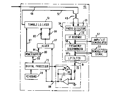
Referring now to FIG. 2, there is shown a diagram of a random-
access digitally-tuned coherent optical receiver 45, which receives the
multiplexed optical carriers by way of an optical fiber 48. This optical
receiver 45 can be used for each one of the receiving stations 2B,27,28 and
2~ of FIG. 1. In FIG. 2, the optical receiver 45 includes a distributed Bragg
35 reflector laser 51 which produces a tunable single local oscillator frequency
,
f/~ ~
2 ~ ~ 3 ~
- 5 -
signal that is coupled into an optical fiber, or guide 52. The output of a
single frequency laser is essentially in a single longitudinal mode. An optical
coupler 49 combines the selected local oscillator optical frequency signal
from the guide 52 with the multiplexed optical carriers on the optical fiber
5 48. The combined optical signals on both fibers 48 and 52 are applied to an
essentially electronic arrangement 54 that stabilizes a set of spaced optical
local oscillator frequencies of the laser 51 by using the spaced set of carriersof the multiplexed signal received on the fiber 48.
In the arrangement 54, the combined signals are heterodyned by
10 a photodetector 55. The resulting heterodyned signal is an electrical signal
that is filtered by an intermediate frequency filter that is located in an
intermediate frequency receiver circuit 56. This intermediate frequency
receiver circuit 56 produces a selected intermediate frequency channel
including any information signal. An amplitude sensitive demodulator 57
15 responds to the selected intermediate frequency channel to produce a
baseband information channel if an amplitude shift keying (ASK)
information signal is utilized.
For the amplitude shift keying arrangement, a fraction of the
selected intermediate frequency channel signal is used for generating an
20 error signal to control the frequency of oscillation of the local oscillator laser
51. That fraction of the selected intermediate frequency channel signal is
applied to a frequency discriminator circuit 58 that is centered at the
intermediate frequency fiF-
If another information signal scheme, such as frequency shift
25 keying, is utilized, then the entire selected intermediate frequency channel
is applied to the frequency discriminator circuit 58. The selected
intermediate frequency channel is a demodulated baseband information
- channel for the frequency shift keying (FSK) information signals, as shown
in block 5~.
No matter which information signal format is used, the output of
the frequency discriminator circuit 58 is filtered and amplified through a
low pass filter and amplifier 60 into an error signal on a lead 61. Thus the
arrangement 54 generates, on the lead 61, an error signal that is used for
locking the local oscillator laser frequency to the selected optical frequency.
3 ~ ~ ~
- 6 -
In the system ofFIG.l, there is a need to guarantee that the
lasers of the receivers will operate at the desired, or selected, local oscillator
frequencies.
FIG.3 presents a curve 62 that is a plot of the power spectra of
5 several multiplexed optical channels vs frequency. The channel energy is
shown centered around carrier frequencies fl, f2, f3 and f5. Desired optical
local oscillator frequencies for the laser 51 of FIG. 2 are offset from the
carrier frequencies by an intermediate frequency fiF, as shown in FIG. 3.
In FIG. 4, a curve representing an error signal 63 is plotted on a
10 horizontal axis of local oscillator frequencies which are aligned with the
carrier frequencies shown in FIG. 3. Error signal 63 makes both positive
and negative polarity excursions within each band of frequencies, defined by
the limits of each received channel 1, 2, 3 and 5 of FIG. 3. It is noted that
the error signal 63 has a zero crossing at each local oscillator frequency
15 fl1, fl2, fl3 and fi5 that is to be used for receiving the respective received
channels 1, 2, 3 and S. Also it is noted that the low pass filter and amplifier
60 of FIG. 2 inserts an offset voltage to the error signal 63 so that the flat
portions of the error signal are slightly above zero. The reason for this
offset voltage will become clear subsequently.
During regular operation of the optical receiver 45 of FIG. 2, a
digital processor 75 is given a desired channel selection, e.g., channel 1, fromthe available channels 1, 2, 3 and 5. The processor 75 causes a power
supply 80 to apply an appropriate bias current or control signal to the laser
51. This bias current is the current value which will cause the laser 51 to
25 oscillate at the local oscillator frequency fll of FIG. 4. A set of such
appropriate bias currents is determined for the set of desired local oscillator
frequencies fl1, fi2, fl3 and fl5 and is stored in the digital processor 75 of
FIG.2.
Referring now to FIG.5, there is shown a solid line laser
30 characteristic curve B5. Heavy dots on this curve represent the values of
laser bias current required to operate the local oscillator laser 51 of FIG.2
at the frequencies fil, fl2, fi3 and îî5, shown in FIG. 4, or at any other
desired carrier frequency within a very wide band.
When the optical receiver 45 of FIG.2isfirst operated, it
35 operates along the laser characteristic curve 65 of FIG. 5. Values of laser
drive current il, i2, i3 and i5 for the desired local oscillator frequencies
.
' .: '
.
,- '
~ ~ 3
fll, fl2, fl3 and fl5 are determined and are stored in the processor 75 of FIG.
2 for subsequent use as the values of laser bias current for determining the
desired optical local oscillator frequencies.
For any selected laser, there is a known operating curve.
5 Similarly the optical carriers are known frequencies fl, f2, f3 and f5, as
shown in FIG. 3. Information representing the laser operating curve of FIG.
5 is stored in the digital processor 75 of FIG. 2. A set of specific addresses
are reserved for storing the values of laser bias current which produce the
desired local oscillator frequencies. The relevant values of laser bias current
10 for producing the local oscillator frequencies are determined as follows by a calibration process.
A first local oscillator frequency is selected. From the known
laser characteristic curve, an initial laser bias current is selected. The valueof that initial laser bias current or control signal is selected to produce a
15 frequency slightly below the first local oscillator frequency, e.g., fil. From a
keyboard 7~ of FIG. 2, the value is put into the digital processor 75 and is
read out to the power supply 80 which applies the appropriate value of
current by way of a lead 81 to an input of adder 82. That current is divided
appropriately by resistors 83 and 84 and the portions are applied
20 respectively to the phase control and distributed Bragg reflector regions of
the laser 51. Power supply 80 also directly supplies a constant bias current
through a lead 87 to the active region of the laser 51.
The local oscillator laser operates at one intermediate frequency
interval from the selected channel frequency.
Since the laser free-running frequency is not at the desired local
oscillator frequency, the feedback loop produces an error signal on the lead
~1. On a lead 8~, an active integrator 70 produces an incremental laser bias
current or control signal error which is applied to another input of the
adder 82. This incremental laser bias current or control signal error is
30 added to the initially selected lsser bias current or control signal and is
applied through the resistors 83 and 84 to the laser 51 driving its free-
running frequency to oscillate at the desired local oscillator frequency, e.g.,
Il -
The digital processor measures the incremental laser bias current
35 in the lead 8~, adds it to the initial laser drive current, and stores the total
as a new value of laser bias current or control signal for the local oscillator
2 ~
-- 8 --
frequency fll.
Similarly an appropriate laser bias current is determined for each
of the other desired local oscillator frequencies fl2, fl3 and fl5. The values of
those bias currents are stored by the digital processor for subsequent
5 retrieval.
During regular operation, the operator selects the desired local
oscillator frequency by inputting a selection through the keyboard 79 to the
digital processor. The processor initializes the active integrator 70 and
applies a request for the appropriate value of laser bias current through a
10 lead 90 to the power supply 80, which supplies that value of laser bias
current through the adder 82 and resistors 83 and 84 to the laser 51. As
long as the laser characteristic has not drifted, the laser operates at the
desired local oscillator frequency, and no error signal is generated on the
lead 61. No incremental laser bias current is generated on the lead 8~ by
15 the active integrator 70.
As a result of device aging or as a result of environmental
changes, the laser characteristic curve may change to a different position,
for example, as presented by an alternative dashed line characteristic curve
67 of FIG. 6. When the environment of the laser 51 shifts the operating
20 characteristic to the alternative characteristic curve 67, applying the
predetermined values of bias current from the original laser characteristic
curve 65, will cause an incorrect laser frequency to be selected. Because
such changes are expected to occur in the position of the laser characteristic
over any long duration of operation in the field, the circuitry included in the
25 laser feedback control loop operates to correct for those changes.
In FIG. 2 a servo-control circuit includes the active integrator 70
which responds to the error signal, for example the error signal on the lead
61, and to signals from the digital processor 75. This servo-control circuit
includes a switch 76 placed across a capacitor 78. Charging and discharging
30 of the capacitor 78 is controlled by signals to the switch from the digital
processor 75.
Activation of frequency locking is initiated by closing the switch
76 and discharging the capacitor 78. Once the capacitor 78 is discharged,
the frequency locking operation is commenced by opening the switch 76.
35 For a selected laser bias current or control signal that produces a laser free-
running frequency, the laser frequency varies during the locking process in
~ .
-- 2~ ~ 31~
g
response to the error signal on the lead 61. As shown by the curve 63 of
FIG. 4, the error signal on the lead 61 crosses zero at the local oscillator
frequencies fl1, fl2, fl3 and fl5. From either side of each of those zero
crossings the polarity of the error signal is appropriate to drive the laser to
5 the desired local oscillator frequency. In response to the error signal on thelead 61, the active integrator circuit 70 commences to charge the capacitor
78 and develop the incremental bias current or control signal error on the
lead 89. This incremental bias current is added by the adder 82 to the
selected laser bias current on the lead 81. The resulting total laser bias
10 current drives the laser to oscillate at the desired local oscillator frequency.
The frequency function i9 the frequency produced by the laser bias current
selected from the power supply 80 in response to the digital processor 75
plus the integral of the error signal and the offset voltage.
When the laser free-running frequency is oscillating at the
15 desired local oscillator frequency, no error current is produced. The digital processor measures, reads or otherwise determines the value of the
incremental laser bias current or control signal error in the lead 8~, adds it
to the presently stored value of bias current or control signal, and then
stores the new total bias current for sub~equent retrieval of a laser drive
20 current for that selected local oscillator frequency.
Inclusion of the active integrator 70 of FIG. 2 extends the pull-in
range of the circuit beyond the steep slope between peaks of the error signal
63 of FIG. 4 at the zero-crossing fll. The pull-in range is extended to the
entire range acros~ each of the defined channels. Because of the offset
25 current, or voltage, the frequency locking arrangement avoids frequency
sticking, or a very long pull-in time which can otherwise be caused by the
low amplitude of a non-offset error signal. Additionally the processor can
determine by the magnitude of the error signal when there is a missing
channel or missing channels.
Each local oscillator frequency has a capture range that equals
the frequency range between zero-crossings, 64.
Importantly, the just described feedback loop of FIG. 2 informs
the digital-processor 75 of any drift of the laser operating characteristic.
For instance, by reference to FIG. 6, the characteristic may drift from the
35 initial characteristic curve 65 to the alternative characteristic curve 67.
When the incremental laser bias current occurs in the lead 8~ of FIG. 2
2 ~
- 10-
causing the digital processor 75 to recalculate the value of stored bias
current il, e.g., il of FIG. 7, for the selected local oscillator frequency, e.g.,
fl, the displacement of the curve 67 of FIG. 6 shows that all of the other
stored values of laser bias currents i2, i3 and i5 would fail to produce the
5 desired local oscillator laser frequencies f2, f3 and f5, respectively. Using the
stored characteristic curve data and the known incremental laser bias
current, the digital processor 75 calculates and stores new values of laser
bias currents i2, i3, and i5 for the frequencies f2, f3 and f5, respectively, asshown in FIG. 7. Thereafter when any desired local oscillator frequency is
10 selected for use, the digital processor 75 will cause the laser bias current
supplied to the laser to be very close to the correct value for the desired
local oscillator frequency.
The foregoing describes an embodiment of a random-access
digitally-tuned coherent optical receiver. This embodiment together with
15 others, which are obvious in view thereof, are within the scope of the
appended claims.