Note: Descriptions are shown in the official language in which they were submitted.
n .~ a1 %'1 'A
~J .:2 :.7 ~.3 ~~-
- 1 -
RD-18,593
Back t"OLrid Of the TI1V nt i nn
Fi_pl_d Of th Tnvantinn
The present invention relates to semiconductor
devices, and more particularly, to improvement of the
operating characteristics of FETS, IGBTs and MCTs.
Background of the Inv nt~nn
In an FET in which an N+ source region is spaced
from an N type drift/drain region by a P type body region
with an insulated gate electrode disposed over the P type
body region and extending from the source region to the
drift/drain region, a parasitic NPN bipolar transistor is
disposed in parallel with the desired field effect
transistor. A first main electrode is disposed in ohmic
contact with the source and body regions and a second main
electrode is disposed in ohmic contact with the drain region.
In this parasitic bipolar transistor, the N type source
region functions as an emitter, the P type body region
functions as the base region and the N type drain region
functions as the collector and the emitter/base function is
shorted. During FET turn-off of an inductive load, this
parasitic NPN transistor can become conductive and have a
detrimental effect on the operation of the field effect
transistor or result in its destruction. In circuits in
which the body/drift region PN junction (an inherent diode)
becomes forward biased, there is a substantial hole current
in the P type body region extension beneath the source
region. This current, in combination with the relative high
resistance of that portion of the body region, can produce a
sufficient voltage drop to forward bias the source/body
junction far from the first main electrode contact which
RD-18,593
shorts that junction. When that portion of the source/body
PN junction injects carriers, the NPN parasitic transistor
becomes conductive, which can destroy the device. In power
FETs, a large gain in this parasitic NPN transistor has an
adverse effect on the ruggedness of the FET because the
larger the gain of this NPN transistor, the smaller the
current required to turn it on and the smaller the safe
operating area of the FET is. The safe operating area is the
combination of current and voltage which the FET can
withstand during the process of turning off without
destruction of the device. At a given voltage, increasing
the current through the FET to more than the maximum SOA
value for that voltage leads to breakdown of the device.
Similarly, increasing the voltage at a fixed current level to
more than the SOA maximum voltage for that current also leads
to breakdown of the device which prevents the device from
turning off. Such breakdown can also result in destruction
of the device. For these reasons, it is considered desirable
to minimize the gain of the parasitic NPN transistor in power
FETs. The gain of this NPN transistor depends on the doping
level of the P type body region. The higher the doping level
of the P type body region, the lower is the gain of this NPN
transistor. Consequently, in order to minimize the adverse
effect of this parasitic NPN transistor, it is desirable to
dope the body region as heavily P type as possible.
Unfortunately, heavy doping of the body region has an adverse
effect on the operation of the desired field effect
transistor, That is, increasing the doping level of the P
type body region increases the threshold voltage of the N
type channel extending through the P type body region from
the source to drain region, i.e. the gate voltage necessary
to render that channel conductive to electrons.
It is known in the prior art to heavily dope the P
type body region and to counter dope just the channel portion
' y ~~i r~ '9 ~~
- 3 -
RD-18,593
of the body region by implanting N type dopant material into
the surface of the body region to reduce its net P type
doping level to adjust the threshold voltage of the field
effect transistor independent of the doping level of the P
type body region.
The presence of this parasitic NPN bipolar
transistor does not have any significant effect on the ON-
state operation of the field effect transistor. It is only
during turn-off of the field effect transistor in the
presence of an inductive load or during turn-off of the
inherent diode that this parasitic NPN bipolar transistor has
an effect on the operating characteristics of the device.
Thus, this parasitic bipolar transistor only affects the
operating characteristics of a field effect transistor if
that field effect transistor is a power device which will be
operated near the limits of its safe operating area.
An insulated gate bipolar transistor (IGBT) is
similar in structure to an FET, except that a P+ collector
region is disposed between the N type drift region and second
main electrode. Consequently, an IGBT contains a similar
parasitic NPN bipolar transistor. However, this parasitic
NPN transistor does not affect the SOA of the device because
it is the lower or PNP transistor which limits device SOA.
Rather, in the IGBT, this parasitic transistor affects the
main current level at which the IGBT latches in the ON-state.
The larger the gain of this parasitic NPN transistor, the
lower the latching current of the rGBT becomes. As is well
known, the IGBT is intended to be a non-latching device and,
therefore, such decreased latching current is undesirable.
Consequently, it is desirable to minimize the gain of the
parasitic NPN transistor in an IGBT in order to maximize the
latching current of the IGBT. The same techniques may be
used to minimize the gain of the parasitic NPN transistor in
an IGBT as are used in FETs. Thus, the only reason for
c~ c; .., n s1 ,1 ..,
Cd '~' ."_ E.j P.9 '.a ~:.'
- 4 -
RD-18,593
reducing the gain of the parasitic NPN transistor in an IGBT
is to increase latching current.
An MOS controlled thyristor (MCT) incorporates a
field effect structure designed to carry current from the N
type base region directly to the first power electrode to
bypass the P type emitter/N type base region junction of the
thyristor and thereby interrupt the regenerative action in
the thyristor to turn it off. Introduction of this field
effect structure creates what is in effect a field effect
transistor of the N+ source region of the turn-off structure,
the P type emitter region of the thyristor and the N type
base region of the thyristor. This structure includes a
parasitic NPN bipolar transistor. By analogy to the IGBT,
decreasing the gain of that parasitic NPN bipolar transistor
is expected to increase the latching current of the MCT,
which is undesirable since the MCT is intended to latch on in
the ON-state. Consequently, the prior art provides no reason
to attempt to reduce the gain of this parasitic NPN bipolar
transistor.
Consequently, the prior art provides no teaching or
suggestion for heavily doping the portion of the P type
emitter region of an MCT in the vicinity of the turn-off
channel of the MOS structure in combination with counter
doping of that channel. The prior art incentives fox such
structures in FETs or IGBTs are not applicable to MCTs
because the problems that structure ameliorates in FETs and
IGBT do not exist in the MCTs.
It has become desirable to operate circuits
including MCTs at as high a frequency as possible, in such
systems as dc-to-do power converters. Consequently, new MCT
structures which facilitate operation at higher frequencies
are desirable.
With the advent of trench gate FETs and IGBTs,
control of the gain of the parasitic NPN bipolar transistor
~ ra 'i « so r
~i ~~ e~ e~ ~~ a
- 5 -
RD-1$,593
has been one of the considerations in the trade-off decision
as to whether to use a trench structure or a planar structure
because ion implantation counter doping of the channel
portion of the body or base region of a trench gate device is
S not possible because the trench walls are normally
perpendicular to the major surface of the wafer whereby ion
implantation ions are traveling parallel to the trench walls
and thus do not implant in the body or base region. Since
counter doping is not possible, a designer, in designing a
trench gate FET or IGBT, must choose between a high threshold
voltage with a low gain parasitic NPN transistor and a low .
threshold voltage with a high gain parasitic NPN transistor.
Consequently, an improved structure for minimizing the gain
of the parasitic NPN transistor in FETs and TGBTs, especially
trench gate versions is needed, as is a method of providing
such a structure.
While it is known that indium and aluminum are P
type dopants, it is standard practice in the semiconductor
industry to avoid using indium and aluminum as dopants in
silicon because their small segregation coefficients lead to
unpredictability of a process to obtain a desired structure.
Use of boron as a P type dopant produces device structures
and characteristics which are quite predictable. The reasons
behind the essentially exclusive use of boron as a P type
dopant are discussed in "The Theory and Practice of
Microelectronics" by Sorab K. Ghandi published by John Wiley
& Sons, especially in the "Choice of p-type Impurity"
section. While there is much literature on the
characteristics of boron and phosphorous as dopants in
silicon, there is much less literature dealing with the use
of indium and aluminum to create P type doped regions. An
article entitled "Diffusion of Indium in Silicon Inert and
Oxidizing Ambients", by D.A. Antoniadis et al., which
appeared in the Journal of Applied Physics, Volume 53, No.
CA 02013349 2000-05-29
RD-18, 593
-6-
12, December 1982, pages 9214-9216 presents data on the diffusion
characteristics of
indium and concludes that indium has a segregation coefficient of 0.1.
Those skilled in the semiconductor art rely on established, controllable
processes for the fabrication of devices because of their established,
relatively high
yields, rather than experimenting with processes which are knows to be
difficult to
predict or control, unless there is a clear incentive for the use of the
"unpredictable"
process. There has been no such incentive for the use of indium or aluminum as
dopants in silicon in the fabrication of field effect devices because of the
availability
and established techniques for controlling ion implantation of the counter
dopant
1o material in the channel portion of the body region to control the threshold
voltage of
the insulated gate structure in the presence of heavy body region dopant
concentrations.
Objects of the Invention
15 Accordingly, a primary object of the present invention is to provide an
improved structure for controlling the threshold voltage of FETs and IGBTs
having
trench gates.
Another object of the present invention is to provide an MCT structure having
a faster turn-off than prior art MCT structures.
2o Another object is to provide an improved method of fabricating FETs, IGBTs
and MCTs.
Summary of the Invention
In accordance with the above objects and others which will become apparent
25 from the specification as a whole, including the drawings, an FET is
provided with a
heavily doped P type body region and a more lightly doped channel region by
doping
the body region with one or more of indium,
r~ y,
(,e, .j~ ~ .~3 z3 'ui x~
- 7 -
RD-18,593
aluminum and gallium or a combination of dopants including
boron and one or more of indium, aluminum and gallium.
Indium and aluminum are depleted in the body region adjacent
the gate oxide because indium and aluminum both have small
silicon/silicon dioxide segregation coefficients. The
concentration of gallium is substantially reduced because of .
its higher diffusion rate in the oxide. The resulting
structure is functionally equivalent to counter doping of the
channel where only boron has been used to dope the base
region. However, unlike counter doping, this technique is
equally effective fox trench gate structures and planar
structures. Consequently, it is a substantial advance over
the use of ion implantation counter doping ~'nce it provides
independent control over body doping level and threshold
voltage in trench gate devices.
Use of a combination of boron and one or more of
aluminum, indium and gallium as the base dopant in an IGBT is
similar in providing the same benefits provided by counter
doping the channel portion of the base region.
We have found that in an MCT, providing a heavily
doped P type emitter region along with a low threshold
voltage channel in the MOS turn-off structure in that emitter
region provides a substantial improvement in the MCT's
operating characteristics, in particular, by providing a much
more rapid turn-off of the device upon application of a turn-
off voltage to the insulated gate. This newly desirable
structure may be provided either by doping the P type emitter
region with a combination of boron and one or more of indium,
aluminum and gallium or by counter doping the channel portion
of that P type emitter region of a surface gate device to
provide a low threshold voltage along with a heavy doping of
the emitter region everywhere except in the channel itself.
f9 .n C~
~aI ~ .:u R:' i.~ _
-
RD-18,593
~rl2f DeSC,~'i_~~ O thP~ Drawi ncrS
The subject matter which is regarded as the
invention is particularly pointed out and distinctly claimed
in the concluding portion of the specification. The
invention, however, both as to organization and method of
practice, together with further objects and advantages
thereof, may best be understood by reference to the following
description taken in connection with the accompanying
drawings in which:
Figure 1 illustrates a prior art surface gate,
vertical FET structure;
Figure 2 illustrates a prior art trench gate, vertical
FET;
Figure 3 illustrates a surface gate, vertical FET
structure in accordance with the invention;
Figure 4 illustrates a trench gate, vertical FET in
accordance with the invention;
Figure 5 illustrates a prior art surface gate
vertical IGBT structure;
Figure 6 illustrates a prior art trench gate,
vertical IGBT;
Figure 7 illustrates a surface gate, vertical IGBT
in accordance with the invention;
Figure 8 illustrates a trench gate, vertical IGBT
in accordance with the present invention;
Figure 9 illustrates a prior art surface gate,
vertical MCT structure;
Figure 10 illustrates a trench gate, vertical MCT
structure;
Figure 11 illustrates a surface gate, vertical MCT
in accordance with the present invention; and
Figure 12 illustrates a trench gate MCT structure
in accordance with the present invention.
as p
~r ~i '.~a. ~ ~;~
- 9 -
RD-18,593
Detailar3 D2SCrintinn
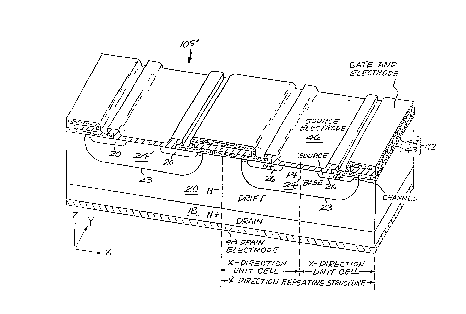
In Figure 1, a prior art vertical surface gate
power field effect transistor is illustrated generally at lOS
in a perspective cross-section view. In this specification,
the adjective "vertical" when used to modify a device, as in
a "vertical FET", refers to the fact that in the device
structure, the current flows through the chip between what
were the top and bottom surfaces of the wafer, as opposed to
flowing laterally or substantially parallel to the wafer's
major surfaces. This device comprises a body of
semiconductor material having a heavily doped N type (N+)
drain region 18 adjacent its lower major surface, a lightly
doped N type (N-) drift region 20 contiguous with the upper
surface of the drain region 18 and extending to the upper
major surface of the semiconductor body. A heavily doped P
type (P+) body region 24 extends into the drift region 20
from the upper surface of the semiconductor body. A lightly
doped P type (P-) body region extension 22 extends into the
drift region 20 from the upper surface of the semiconductor
body and is contiguous with, but extends laterally from the
P+ main potion 24 of the body region. A heavily doped N type
(N+) source region 26 extends into the P+ main portion 24 of
the body region arid into the P- body region extension 22 from
the upper surface of the semiconductor body. This results in
the complex PN junction configuration 21 between the body and
drift regions. An insulated gate electrode 42 is disposed on
the upper surface of the semiconductor body and extends from
in alignment with the source region 26, across the body
region extension 22 and into alignment with the drift region
20 to control the conductivity for electrons of a channel
portion of the body region extension 22. A first main
(source) electrode 46 is disposed on the upper surface of the
semiconductor body in ohmic contact with the source region 26
and the main potion 24 of the body region. A second main
.~ a ~ ~~
~, rsi' .d t:'J z.f i
- 10 -
RD-18,593
(drain) electrode 48 is disposed on the lower surface of the
semiconductor body in ohmic contact With the drain region 18.
As illustrated in Figure 1, the device lOS
comprises a plurality of unit cells, each of which extends in
the Y-direction in the figure(an XYZ coordinate system is in
the lower left portion of the figure) with a plurality of
unit cells distributed in the X-direction. As indicated in
the figure, adjacent X-direction unit cells are mirror images
of each other and an X-direction repeating structure
comprises two unit cells. If desired, the source region 26
in one of the unit cells of the X-direction repeating
structure may be omitted, in which case, the X-direction
repeating structure is also a unit cell.
Inherent in the structure 10S is an NPN bipolar
transistor having an emitter region 26, a base region 24/22
and a collector region 20/18. This bipolar transistor is
often referred to as a parasitic transistor because (1) its
presence is not desired, even though it is inherent in the
field effect transistor structure, and (2) it is detrimental
to the operation of the field effect transistor if it becomes
conductive. It is to prevent this parasitic NPN bipolar
transistor from becoming conductive that the main portion 24
of the body region is heavily doped P type material, since an
N+/p+ junction has a lower emitter injection efficiency than
an N+/p junction and, therefore, tends to produce a low gain
transistor which is less likely to become conductive than a
high gain transistor. The body region extension 22 is
lightly doped P type material in order to provide the surface
channel with an acceptably low threshold voltage for
rendering the channel conductive to electrons.
Unfortunately, this low doping level in the body region
extension forms a second portion of the parasitic NPN bipolar
transistor which has a higher gain than the portion involving
the P+ main portion of the body region. It is this second
~.a h'~ .n: " ~,
-~,, z.~ ~ 3 '.x 2.i
- 11 -
RD-18,593
portion of the parasitic transistor which becomes conductive
first and thus, it is this portion which limits the turn-off
operating characteristics of the field effect transistor.
FETs of this type are normally fabricated by first diffusing
the body region extension 22 of the body region through a
window in the gate oxide followed by diffusion of the P+ main
portion 24 of the body region through the same window in the
gate oxide. This is followed by blocking of the middle of
that window to create two separate windows along the edge of
the gate oxide through which source regions 26 are
subsequently diffused to create the illustrated structure.
Thereafter, the surface of the body region
extension portion 22 is counter doped by ion implantation
through the gate oxide 43. While this structure allows the
main portion 24 of the body region to be heavily doped P type
and the body region extension portion 22 more remote from the
surface to be moderately doped, it still leaves the body
region extension portion 22 less heavily doped than the P+
main portion 24 and leaves the portion of the parasitic
bipolar transistor which includes the body region extension
as a relatively high gain bipolar transistor. This is a
particular problem in the case of a trench gate structure
such as that illustrated in Figure 2 at lOT in which the body
region extension portion 22 of the body region is the same
length (vertically) as the base region itself, since for a
short channel device, the body region becomes very thin and
results in ~ high gain parasitic NPN transistor comprising
the source region 26, the body region extension portion 22 of
the body region and the drift/drain region 20/18. This
contrasts with the planar gate electrode structure
illustrated in Figure 1 wherein most of the body region
portion of the NPN bipolar transistor is substantially
thicker than the length of the channel. Further, with the
trench gate structure illustrated, it becomes impossible to
~, ~'v '~'";~ ;
Y,d ~W ~:~" r..I ....: ..
12 °
RD-18,593
counter dope the surface of the body region extension 22 to
reduce the threshold voltage because of the vertical nature
of the trench wall at that location. However, the PN
junction 21 still has a complex configuration.
We have found that.the fabrication of FETs can be
improved by eliminating the separate doping of the body
region extension and forming the P+ portion of the body
region 24 by use of one or more of indium, aluminum and
gallium or a combination of boron and one or more of indium,
ZO aluminum and gallium to provide the structure lOS' shown in
Figure 3 in which the PN junction 23 between the drift region
20 and the body region 24 has a much simpler configuration.
This is because of the small silicon/silicon dioxide
segregation coefficients for indium and aluminum and the
higher diffusion rate of gallium in silicon dioxide.
Consequently, the pre-diffusion of the body region extension
portion of.the body region may be dispensed with and the P+
main portion of the body region may be diffused directly,
thereby providing a simple PN junction contour 23. However,
if one of the dopants diffuses significantly faster than the
other in silicon, it is considered desirable to diffuse the
slow diffuser first so that the two dopants will diffuse to
the same depth. There are some indications that indium alone
does not form a good PN junction. Consequently, we prefer to
use a combination of boron and indium rather than indium.
Use of a combination of boron and indium also has the benefit
of assuring the formation of a high quality ohmic contact
between the body region and the source electrode.
This doping technique results in the formation of a
P type body region which is heavily doped everywhere except
adjacent the surface under the gate oxide where the small
segregation coefficient of the indium or aluminum essentially
totally depletes the surface portion of the silicon of the
indium or aluminum dopant, thereby leaving only the boron
- 13 -
RD-18,593
dopant. The concentration of the boron is selected to
provide the desired threshold voltage, while the
concentration of the indium or aluminum is selected to
provide the desired overall P type doping level in the
remainder of the body region. This effectively suppresses
the parasitic NPN transistor. This suppression is achieved
at the expense of the use of a fabrication process which is
relatively unpredictable and which requires trial and error
fine tuning to obtain dopant concentration and fabrication
sequences which result in a device having the desired doping
levels in the appropriate locations. It may also be
desirable to provide a more heavily boron doped region at the
electrode contact surface.
In the trench structure lOT' shown in Figure 4, a
further substantial advantage which results from this
fabrication process is the fact that the growth of the gate
oxide on the sides of the trench inherently depletes the
channel portion of the body region of the aluminum, indium or
gallium dopant, without any need for ion implantation of
counter doping into the vertical trench wall. Further, since
the body region itself is formed by diffusion into an
existing N type region 20 and the source region 26 is formed
by diffusion into the body region 24, the depletion of the
indium, aluminum or gallium at the gate oxide surface has the
effect of shortening the channel portion of the body region
due to an inward contraction into the body region of the
local interfaces between the P type body region and the N
type drift region and N type source region. The PN junction
23 is otherwise disposed in a single plane. Consequently, in
this trench gate structure, the channel portion of the body
region is shorter (vertically) than the body region a
slightly greater distance from the trench surface. As a
consequence, this structure is more effective in suppressing
:"~ 'j ~ s i ~ f':t
l.~ ~ .d c : >.) '~ .~
- 14 -
RD-18,593
the parasitic NPN bipolar transistor than is the prior art
structure.
A surface gate insulated gate bipolar transistor
(IGBT) is illustrated generally at 1105 in Figure 5, while a
trench gate prior art IGHT 110T is shown in Figure 6. The
device 110S is structurally similar to or identical to the
prior art field effect transistor lOS except for the presence
of a heavily doped P type (P+) region 128 adjacent the lower
surface of the semiconductor body in place of the N+ drain
region. In Figures 5 and 6, reference numerals in the 100's
are used. In general, reference numerals ending in the same
two digits in the figures identify related structure which
may not be discussed in full here. The details of the device
fabrication process and structure may also be adjusted in
order to optimize the operation of the insulated gate bipolar ,
transistor.
In an IGBT, the region 126 is known as the emitter,
the region 124 is known as the base, the region 120 is known
as the drift region and the region 128 is known as the
collector. In the insulated gate bipolar transistor, the
same parasitic NPN bipolar transistor is present as is
present in the field effect transistor. However, its effect
on device operation is substantially different. In
particular, increasing the gain of that parasitic NPN bipolar
transistor has the effect of reducing the main current level
at which the insulated gate bipolar transistor latches in the
ON-state. As is well known in the art, one of the objectives
in insulated gate bipolar transistors is to prevent them from
latching, since when they latch, gate control of the state of
the device is lost. Consequently, the adverse effect of the
parasitic NPN bipolar transistor in an IGBT is a decrease in
the latching current level for the insulated gate bipolar
transistor.
cr ~~ .,~ ~-
,.J a ,,
~ .r w~s
- 15 -
RD-18,593
Our improved device fabrication method and the
structure which results from the use of a combination of
baron and one or more of indium, aluminum and gallium to dope
the base region has the same beneficial effects in
suppressing the gain of the parasitic NPN transistor in the
insulated gate bipolar transistor as it does in an FET. A
surface gate IGBT 1105' in accordance with the invention is
shown in Figure 7, while a trench gate IGBT 110T' in
accordance with the invention is shown in Figure 8. The
devices 1105' and 110T' differ from devices 110S and 110T in
a similar manner to that in which FETs lOS' and lOT' differ
from FETs lOS and lOT. However, as has been noted, the
manner in which this different structure affects the
operation of the insulated gate bipolar transistor is
substantially different than the manner in which it affects
the operation of the field effect transistor, since in the
insulated gate bipolar transistor, the purpose of suppressing
the gain of the parasitic NPN transistor is to raise the
latching current level of the IGBT rather than to maximize
the safe operating area as is the case in the field effect
transistor.
We have discovered a previously unknown effect of
the parasitic NPN bipolar transistor which is introduced into
a thyristor when an MOS controlled channel is introduced to
control turn-off of the thyristor and thereby provide a bOS
controlled ~,hyristor (MCT). A prior art surface gate,
vertical MCT 2105 is shown in Figure 9, while surface gate
and trench gate MCTs in accordance with the present invention
are shown at 2105' and 210T' in Figures 11 and 12,
respectively. Figure 10 illustrates a trench gate MCT 210T
which is made Without using our invention.
While the existence of such a parasitic NPN
transistor is easily recognized by analogy to the FET and
IGBT, neither its effect, nor the magnitude of its effect
c,, Aa .~~ c1 , 7
~i
Id ~ .:d. tJ fd ~: x;~
- 16 -
RD-18,593
have been understood or appreciated in the art.
Consequently, there has been no suggestion or incentive for
doing anything about that parasitic transistor. The known
effects of the parasitic NPN bipolar transistor in the MOSFET
and the IGBT provide no suggestion that that parasitic
transistor will have any adverse effect in the MCT. However,
we have found that increasing the gain of the parasitic NPN
bipolar transistor indirectly increases the turn-off time for
the MCT. This is the result of a series of effects or
considerations. First, in order for the MCT to latch the sum
of alpha (OCp) of the thyristor's PNP (upper) transistor and
the alpha (ocn) of the thyristor's NPN (lower.) transistor must
be greater than 1 where a is the current gain of the
corresponding inherent transistor of the thyristor. In order
to avoid confusion, the inherent PNP and NPN transistors
which create the regenerative action of a thyristor are
referred to herein as the thyristor's PNP transistor and the
thyristor's NPN transistor and the parasitic NPN transistor
is referred to by that name to clearly distinguish the
parasitic NPN transistor from the inherent or main NPN
transistor of the thyristor. The majority of stored charge
in an MCT is in the P type (wide) base region. Consequently,
the turn-off time of an MCT becomes shorter as the lifetime
of carriers in the P type base region decreases because a
shorter lifetime results in more rapid recombination of the
stored charge in that base region during turn-off of the
device. Thus, it is desirable to minimize or "kill" the
lifetime in that P type base region. However, the lower the
carrier lifetime in the P type base region, the lower the an
of the thyristor's main NPN transistor becomes. Thus, the
requirement that Ocn > 1 - ocp places a lower limit on the Ctn
and a lower limit on carrier lifetime in the P type base
region. Thus, if otp can be increased, an and the lifetime in
the P type base can both be decreased further. We have
r
~~e ~~ ~3~
~~.~.~a.~~r:l
- 17 -
RD-18,593
recognized that since ap of the thyristor's PNP transistor is
a function of the emitter efficiency of the thyristor's P
type emitter region, that efficiency must be maximized. We
have also recognized that the parasitic NPN transistor
provides an alternate path fox the flow of electrons from the
N type base region 220 to the main electrode 246 which
contacts the P type emitter region 224. As such, the more
electrons which flow through the parasitic NPN transistor,
the lower the effective emitter efficiency of the P type
emitter region becomes. The primary controller of the
quantity of electrons which flow through the parasitic NPN
transistor is the base transport factor of the parasitic NPN
bipolar transistor. The higher the base transport factor,
the more electrons flow through that transistor. That base
transport factor can be decreased by more heavily doping of
the emitter region extension portion 222 of the P type
emitter region of the MCT. Consequently, suppressing the
gain of the parasitic NPN transistor in the MCT structure
allows the turn-off time to be decreased and thus increases
the speed of the MCT. This relationship between the speed of
the MCT and the characteristics of the parasitic NPN
transistor is unrecognized in the prior art, and
consequently, the prior art provides no suggestion for
providing a heavily doped P type emitter region extension and
a counter doped channel in an MCT. We have determined form
measurements on actual devices and simulations of them that
as much as 50% of electrons may flow through the P type
emitter region extension in conventional MCTs, thereby
causing a significant adverse effect on the efficiency of the
P type emitter. An even larger percentage of the electrons
may follow that path during turn-off. That electron flow now
appears to be a significant cause of junction avalanche
breakdown which we now recognize as a significant cause of
the failure of MCTs to turn off at high currents.
J
/~d E.3 s', n.a :.'v ~_'~ ..
- 18 -
RD-18, 593
Our discovery, for the first time, provides an
incentive for heavily doping the emitter region extension and
counter doping the channel portion of the P type emitter
region extension in an MCT. That is, essentially eliminating
the emitter region extension. Use of the combination of
boron and one or more of aluminum, indium and gallium as a
dopant for the P type emitter region of the MCT provides the
benefit of providing a low doped channel portion of a heavily
doped P type emitter region in an MCT, independent of whether
the channel is located along the planar surface of the
semiconductor body or along a sidewall of a trench containing
a gate electrode. These improved operating characteristics
are also provided in the MCT by use of counter doping to
adjust the MOS threshold of a heavily doped emitter region.
The benefits of having a heavily doped emitter region with a
counter doped or lightly doped channel are equally applicable
in complementary MCTs in which the MOS turn-off structure
includes a P+ source region disposed in the N type emitter
region.
While each of the devices illustrated and described
is a vertical device, the invention is also applicable to
lateral devices.
While the invention has been described in detail
herein in accord with certain preferred embodiments thereof,
many modifications and changes therein may be effected by
those skilled in the art. Accordingly, it is intended by the
appended claims to cover all such modifications and changes
as fall within the true spirit and scope of the invention.