Note: Descriptions are shown in the official language in which they were submitted.
201~311
The present invention relates to a semiconductor device
package and a sealing apparatus and method therefore and,
more particularly, hermetic seal of a semiconductor device
chip together with an inert gas in a package body upon
adhesion of a lid to the package body with an adhesive.
A semiconductor ~evice package generally comprisss a
rectangular package body and a rectangular lid adhered to it.
In a conventional semiconductor device package, an adhesive --
0 i8 applied to an adhesion layer (plating layer) of a package
body, a lid is urged against a package body while the entire
structure is being heated to perform an adhesion operation.
By this operation, the hermetic seal of the package body can
be achieved, and the semiconductor device chip is sealed in
the package. In this case, a sealing solder is generally
used as an adhesive.
The hermetic seal of the package is performed to protest
semiconductor device chips from conta~ination sources (e.g.,
dust, chemicals, gases, and humidity) which adversely affect
~ : .
. ~ ,.
~ '
:
- 1 -
.~ . .
2014311
semiconductor device chip and from mechanical damage. Each
semiconductor device chip must be, therefore, sealed in a
package with an inert gas and must be protected with the
inert gas.
In a conventional method of adhering a lid with an -
adhesive while being heated under pressure, voids tend to be
left in a hermetic seal portion, as an overlapping portion
between the lid and the plating layer (adhesion layer) of the
package body. A sealed gas inside the package tends to leak
through the seal portion, thus causing sealing defects.
The width of the seal portion must be minimized in
consideration of swelling of the adhesive. In a recent
compact package in which a LN (Low-Noise) FET or the like is
mounted, the seal portion is qetting short. For this reason, ~ -
seal portion defects tend to frequently occur and become a
cause for decreasing a semiconductor device product yield.
The present invention provides a semiconductor device
package capable of reducing defects in a seal portion between
a package body and a lid.
The present invention also provides a sealing apparatus
for semiconductor device package, capable of improving the
adhesion strength between the package body and the lid.
' ~" ..
- ;~ ' , ,~: ,
.t,~- . '' .,~". '
2014'~11
Further, present invention provides a sealing method for
a semiconductor device package, capable of improving the
uniformity of the eutetic reaction by performing scrubbing to
break the surface oxide film formed on the preform such as
S Au;Sn.
-
More particularly, in one aspect of the present
invention, there is provided semiconductor device package
comprising: a package body in which a semiconductor device
chip are mounted: a lid adhered to the package body for
hermetical sealing of the package body: an annular adhesion
layer being formed on the package body, the adhesion between
the package body and the lid being performed by applying an
adhesive between the annular adhesion layer and the lid, and
the hardening the applied adhesion after at least one of the
package body and the lid is pivoted to be coaxial with the
adhesion layer.
:
In a further aspect of the present invention, there is :
provided a sealing apparatus for a semiconductor device
package, for hermetically sealing a package body mounted with
a semiconductor device chip after a lid is adhered to an
annular adhesion layer formed on the package body by using an
adhesive, comprising: a table for supporting the package
body: a lid holding ~ig for holding the lid; urging means for
vertically moving the table and/or the lid holding jig
~:
,,.~,
:
,~; , . . .
.~ ~ ~','.
201~311
such that at least one of the package body and the lid urges
the other of the package body and the lid: and means for
rotating the table and/or lid holding jig such that at least
one of the package body and the lid i~ rotated to be coaxial
with the annular adhesion layer.
In a still further aspect of the present invention,
there i8 provided a sealing method for a semiconductor device
package, comprising: the first step of mounting a
semiconductor device chip on a package body having an annular
adhesion layer formed thereon and of applying an adhesive to
the adhesion layer: the second step of urging at least one of
the package body and lid for hermetically sealing the package
body against the other of the package body and the lid: and
the third step of rotating at least one of the package body
and the lid to be coaxial with the adhesion layer.
~he present invention will become more fully understood
from the detailed description given hereinbelow and the :~
accompanying drawings which are given by way of illustration -
only, and thus are not to be considered as limiting the
pre~ent invention.
Further scope of applicability of the present invention
will become apparent from the detailed description given
hereinafter. However, it should be understood that the
detailed description and specific examples, while indicating
preferred embodiments of the invention, are given by way of
illu~tration only, ~ince various changes and modifications
- 4 -
: -
t~
~ S~
~01~311
within the spirit and scope of the invention will become
apparent to those skilled in the art from this detailed
description.
Fig. l is a sectional cide view of a semiconductor
device package according to an embodiment of the present
invention:
Fig. 2 is a plan view showing a package body for a
semiconductor device package according to the embodiment ~ -
shown in Fig. l;
Fig. 3 is an enlarged sectional view showing an adhesion
state between a lid and a package bod~ in the semiconductor
device package shown in Fig. l;
Fig. 4 is a partially sectional side view of a sealing
apparatus for a semiconductor device package according to the
embodiment of the present invention; and
Fiq. 5 is a plan view showinq an overall structure of
the 6ealinq apparatus for a semiconductor device packaqe
accordinq to the embodiment of the present invention.
A compact ceramic packaqe accordinq to an embodiment of
the present invention will be described with reference to
Figs. 1 to 3.
_ 5 _
. '
-. ~, .
,
-- 2 ~ 1 ~ 3 1
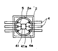
1 As shown in Figs. 1 and 2, a package 1 comprises a
package body 2 ~or carrying a semiconductor device chip
41 and a lid 3 for sealing the semiconductor device chip
41 in the package body 2. This hermetic seal is
per~ormed by adhering the lid 3 to the package body 2.
Six leads are separately provided on the both sides o~
the package body 2. Each lead 4 is ~ormed by coating
gold (Au) on an iron-nickel (Fe/Ni) alloy plate. The
distal end Or an inner lead 4a o~ each lead 4 and each
bonding pad 42 o~ the semiconductor device chip 41 ar~ -
electrically connected by the wire bonding o~ an Au wire
5.
As shown in Fig. 3, an annular plating layer 12
constituting an adhesion layer ~or adhering the lid 3 is
~ormed on the upper edge o~ the package body 2. The
plating layer 2a comprises a nickel (Ni) plating layer
12a and a gold (Au) plating layer 12b $ormed on the Ni
plating layer 12a. Similarly, an annular plating layer
13 consisting o~ an Ni plating layer 13a and an Au
plating layer 13b is ~ormed on the lower edge o~ the lid
3. Prior to sealing o~ the package body 2, a seal-like
adhesive (sealing solder) 10 is placed on the plating
layer 12. The adhesive 10 consists o~ a eutectic alloy -
such as a gold/tin (Au/Sn) alloy. The plating layer 12
has almost the same shape as the plating layer 13.
:
The package body 2 is adhered to the lid 3 as
~ollow8. The adhesive 10 is interpoeed between the
2 ~ 1 ~ 3 1 r
1 plating layers 12 and 13, and the plating layer 12 Or
the package body 2 is urged against the plating layer 13
of the lid 3 while the lid 3 is being heated. In this
case, the adhesive 10 is melted between the plating
layers 12 and 13 to form an annular seal portion 51
consisting of eutectic bonds. In this state, at least
one Or the package body 2 and the lid 3 is pivoted to be
coaxial with the plating layers 12 and 13, thereby
completing adhesion. By this pivotal movement, the
plating layer 12 oi the package body 2 can be per~ectly
adhered to the plating layer 13 o~ the lid 3 to
eliminate voids rrom the seal portion 51.
The outer dimensions of the lid 3 are slightly
smaller than those Or the package body 2. There~ore,
sagging Or the molten adhesive 10 and projections o~ the
hardened adhesive on the side sur~aces o~ the package
body 2 can be prevented.
A package sealing apparatus according to the
embodiment oi the present invention will be described
with rererence to Figs. 4 and 6.
This package sealing apparatus comprises a table
21 and a collet 22 including a heating element. The
package body 2 is placed at the center Or the table 21, ~ -
and the lid 3 is held by the collet 22. The table 21 is -
; arranged to be rotatable, and the lower surrace Or the
table 21 is connected to a link mechanism 23 eccentric
, rrom a rotating shart 21a Or the table 21. The link
,~
:
7 -
2~3~:
1 mechanism 23 comprises an arm 24 and a dise 25. A motor
26 is connected to the disc 25 to rotate the disc 25.
The link meehanism 23 is driven upon rotation o~ the
motor 26, and then the table 21 is rotated. In this
embodiment, the motor 26 is rotated by two revolutions,
and the table 21 is then reciprocated twice within an
angle of 30'.
A reeessed chuck portion 22a is ~ormed in the lower
surraee Or the collet 22. The chuck portion 22a is
connected to a vaeuum pump 27. The lid 3 is chucked in
vacuum by the ehuek portion 22a oY the collet 22 and is
eonveyed onto the package body 2. A hydraulic actuator
28 is eonneeted to the upper end o~ the eollet 22, and
the lid 3 whieh has eonveyed onto the paekage body 2 is
urged against the paekage body 2 by the hydraulie ~-
aetuator 28 during adhesion. In addition, sinee the ~ -
eollet 22 ineludes a heating element, the lid 3 is
heated to be 300'C during adhesion.
The pae~age body 2 and the lid 3 whieh are set on ;~
the table 21 are stored together with the lower portion
Or the eollet 22 in a ehamber 29 provided on the table
21. Nitrogen gas (N2) or a mixture o~ nitrogen and
hydrogen gases (N2 + H2) is supplied to the ehamber 29
as a sealing gas. The adhesion operation is per~ormed
in an inert gas (sealing gas) atmosphere. When the
paekage body 2 is hermetieally sealed by the above
adhesion operation, the semieonduetor deviee ehip 41 -~
' . ...
,',''" ,' .
;
'"'''. '
f "-~! j ,. .':', .' ', i
2~J~3~
1 sealed inside the package 1 is kept in an inert
condition by such a sealing gas.
As shown in Fig. 4, the collet 22 and the hydraulic
actuator 28 are fixed on a support plate 30. This
support plate 30 is mounted at the distal end of a
support arm 31 shown in Fig. 5. The support arm 31 is
~ixed on a vertical pivot sha~t 33, and a counterbalance
32 is mounted at the base end portion of the pivot sha~t
33. A gear 33a is ~ormed at the lower portion o~ the
vertical pivot shaft 33 and is meshed with an output
gear 34a of a drive motor 34. Upon forward or reverse
rotation o~ the drive motor 34, the support arm 31 is
pivoted between a position o~ the table 21 and a ~eed -
position oi the lid 3. A convey path 3~ is ~ormed at
the ~eed position o~ the lid 3, so that the lid 3 is
continuously ~ed along the convey path 35.
An operation o~ the package sealing apparatus will
be described below.
The collet 22 which receives the lid 3 at the
position o~ the convey path 35 is moved to the position
Or the table 21 by the drive motor 34. The package body
2 having the adhesive 10 is placed on the table 21. The
collet 22 is driven to coaxially align the plating layer
13 o~ the lid 3 with the plating layer 12 oi the package
body 2. When this positioning is completed, the
hydraulic actuator 28 i8 driven to move the collet 22 -~
downward, thereby coverin8 the lid 3 on the package body
.
20~3. .-:.
1 2 so as to interpose the adhesive between the plating
layers 12 and 13. Meanwhile, the lid 3 and the adhesive
10 are heated to 300 C by the collet 22, and N2 gas or
the like is supplied to the chamber 29. The lid 3 is
urged against the package body 2 by the hydraulic
actuator 28. When the adhesive 10 is melted by heat,
the table 21 is pivotally reciprocated twice, thereby
completing the adhesion operation. -
When the plating layers 12 and 13 have an annular -
shape and the package body 2 is pivoted twice during -
adhesion, the plating layers 12 and 13 are periectly
adhered to each other. As a result, voids can be
eliminated irom the seal portion 51, and a sealing
property oi the package 1 can be improved. ~
In this embodiment, the package body 2 had a size oi ~ -
1.6 mm X 1.5 mm, and each oi the plating layers 12 and
13 had an outer diameter oi 1.3 mm and an inner diameter
oi 1.1 mm. A preiormed body oi an Au/Sn eutectic alloy
(thickness : 30 ~m) was used as the adhesive 10.
In thiC embodiment, the table 21 is provided.
However, the collet 22 may be pivoted. Alternatively,
the table 21 and the collet 22 may be pivoted relative
to each other.
In this case, as a means ior pivoting the table 21
and the collet 22, ior example, a stepping motor may be
used in place oi a lin~ mechanism used in this
embodiment.
,' - , .
1 0 , . . . .
. .. ' ....