Note: Descriptions are shown in the official language in which they were submitted.
PLAJ : O 1'T
~~ ~ ~_~:'~~v~
BATTERY FOWERED IN~°TWNF AMPIrI~'IIER
This invention relates generally to a battery aperated
in-line audio amplifier and, more particularly, to an audio
amplifier that employs high and low current modes of
operation to extend battery life.
Standard telephones typically do not include any
provision for adjusting the volume of the conversation
presented to the receiver portion of the telephone handset.
Accordingly, where there is a poor connection or the user
is hard of hearing, the volume of the conversation may be
undesirably low. The user has little recourse other than
asking the other party to speak more loudly. Therefor, it
is desirable that the user have available an inexpensive
in-line amplifier that is readily attached to a standard
telephone and adjustable to the user's desired comfort
level. Zn order for the in-line amplifier to be readily
attachable to a standard telephone, it requires access to
an independent source of electrical power. To avoid
modifications of the telephone it is desirable that this
independent electrical power source be in the form of a
readily interchangeable battery.
However, use of a battery as the electrical power
source for the in-line amplifier imposes severe limitations
on the design of the in-line amplifier. For example, an
operational amplifier used in the in-Line amplifier
typically lacks the current driving capability to properly
operate the receiver of the telephone handset beyond
' -2-
relatively low level conversation. Therefor, an output
stage, such as an emitter follower that draws current
directly from the battery, is employed. High quality
reproduction of the audio signal can be achieved by using
a class A output stage, however, class A output stages
typically suffer from low efficiency and high quiescent
currents. It should be apparent that the use of a class A
output stage will severely shorten the life of the battery
and necessitate undesirably frequent changing of the
to battery.
Alternatively, class B output stages are well known
for their high efficiency and low quiescent current draw.
However, class B output stages are equally well known for
the cross over distortion resulting from the dead band
surrounding the zero voltage level. This dead band is, of
course, caused by the complimentarily connected transistors
in a class B output stage being simultaneously biased
"off." Thus, while the battery life of such a device would
be greatly enhanced over class A output stage, the audio
signal presented to the receiver of the telephone handset
would be unacceptably distorted.
Further, it should be appreciated that use of battery
power for the in-line amplifier dictates that the battery
will periodically discharge to such a low level as to be
unable to operate the amplifier. At this point, the
amplifier not only does not amplify the audio signal, but
also blocks the audio signal from being delivered to the
telephone handset. Thus, the user is presented with the
alternatives of removing the in-line amplifier or replacing
the battery so that the telephone is once again operable.
Neither alternative is desirable. Rather, it is preferable
that in-line amplifier should be capable of controllably
enhancing the audio signal without undesirably blocking the
audio signal.
_3_
The present invention is directed to overcoming one
or more of the problems set forth above.
The primary object of the present invention is to
provide an apparatus that amplifies audio signals using
power supplied by a battery, but minimizes the current
required from the battery.
Another object of the present invention is to provide
an audio amplifier that has an extremely low quiescent
current.
Yet another object of the present invention is to
provide an audio amplifier that effectively by-passes the
amplification stage in response to low battery voltage.
Still another object of the present invention is to
provide an audio amplifier that has high and low current
modes of operation in order to extend battery life.
Still another object of the present invention is to
provide an audio amplifier that reduces crossover
distortion caused by the use of a class B output stage.
To attain these and other objectives, an apparatus is
provided for controllably amplifying an audio signal
delivered to a receiver. The apparatus includes a battery
adapted to provide electrical power to the apparatus and a
means for detecting the voltage level of the battery and
delivering first and second signals in response to the
battery voltage being respectively greater than and less
than a preselected level. Further, meant receives the
audio signal and amplifies the audio signal in response to
receiving the first signal. Conversely, means receives the
audio signal and by-passes the amplifier means to deliver
the audio signal directly to the receiver in response to
receiving the second signal.
Other objects and advantages of the invention will
become apparent upon reading the following detailed
description and upon reference to the drawings in which;
Fig. 1 is a general block diagram of the instant
apparatus;
Fig. 2 is a detailed electrical schematic of one
embodiment of the instant apparatus;
Fig. 3 is a graphical representation of the transfer
characteristic of a class B output stage;
Fig. 4 is a graphical representation of the crossover
distortion typically caused by a complimentary emitter
follower.
While the invention is susceptible to various
modifications and alternative forms, specific.embodiments
thereof have been shown by way of example in the drawings
and will herein be described in detail. It should be
understood, however, that it is not intended to limit the
invention to the particular forms disclosed, but on the
contrary, the intention is to cover all modifications,
equivalents, and alternatives within the spirit and scope
of the invention as defined by the appended claims.
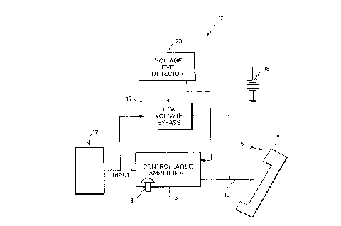
Fig. 1 illustrates a general block diagram of the
apparatus 10. The apparatus 10 has an input line 11
connected to the base of a telephone unit 12 and an output
line 13 connected to a handset 14 and, in particular, to
the receiver portion 15 of the handset 14. .".
-5-
The input line 11 and output line 13 are alternatively
connected together through either a controllable amplifier
16 or a low voltage bypass 17. The apparatus 10 is powered
via a source of electrical energy, such as a battery 18.
The use of the battery 18 dictates that the apparatus 10
periodically discharges the battery 18 to such a level as
to require replacing the battery 18. It is preferable,
therefor, that the apparatus 10 be capable of passing the
audio signal from the base unit 12 to the receiver 15
independent of the state of charge of the battery 18.
Thus, the low voltage bypass 17 is provided as an
alternative connection between the receiver 15 and base 12
when the voltage level of the battery 18 is insixfficient to
properly operate the controllable amplifier 16.
It should be appreciated that the apparatus 10 is
intended for use on telephones of individuals who are hard
of hearing and require additional amplification of the
audio signal in order to properly carry on a telephone
conversation. In order to accommodate adjustment of the
level of amplification, a potentiometer 19 is provided in
the apparatus 10 and is directly accessible by the user of
the telephone to adjust the comfort level of the
amplification. Alternatively, a resistor controlled by a
field effect transistor could be employed to allow for
pushbutton adjustment of the amplification.
In order to determine when the voltage level 18 is at
a minimum operating level, a voltage level detector 20 is
provided. The voltage level detector 20 includes a pair
of outputs connected respectively to the low voltage bypass
17 and the controllable amplifier 16. Ordinarily, when the
voltage level of the battery exceeds the minimum
preselected operating voltage level, the voltage level
detector 20 provides electrical power to the controllable
amplifier 16 so as to allow for amplification of the signal
6 ~~I ~~~~
delivered from the base unit 12 over the input line 11,
When, however, the voltage level of the battery 18 falls to
a level below the preselected minimum operating voltage,
the voltage level detector 20 delivers a control signal to
the low voltage bypass 17 providing a substantially direct
connection between the input and output lines 11, 13.
Further, the voltage level detector 20 also discontinues
delivering power to the controllable amplifier 16 in
response to the battery voltage level falling below the
preselected minimum operating voltage.
Referring now to Fig. 2, a detailed electrical
schematic of the apparatus 10 is illustrated: The low
voltage detector 20 generally includes those elements shown
within the dashed line 20. A pair of serially connected
resistors 22, 24 form a voltage divider network for
determining when the battery voltage level has dropped
below its preselected minimum operating voltage. The
junction of the resistors 22, 24 is connected to the base
of an NPN type bipolar junction transistor 26. The emitter
of the transistor 26 is connected to system ground, while
the collector of the transistor 26 is connected through a
resistor 28 to the base of a PNP type bipolar junction
transistor 30 and to the positive terminal of the battery
18 through a resistor 32. The emitter of the transistor 30
is also connected to the positive terminal of the battery
18, while the collector of the transistor 30 is connected
to the low voltage bypass 17> y
It should be noted that system ground corresponds to
the negative terminal of the battery 28 and to the input
return line connected to the base unit 12. The electrical
connection between the handset 14 and base unit 12 '
typically includes four wires, two of which are connected
to the receiver portion 15 and two of which are connected
to the transmitter portion.
_7_
The low voltage bypass 17 includes a field effect
transistor 34 that has its gate connected to the collector
of the transistor 30, its source connected to the input
line 11, and its drain connected to the receiver 15.
Thus, it should be appreciated that as long as the
voltage appearing at the junction of the resistors 24, 22
is greater than the bias voltage of the transistor 26,
transistor 26 remains biased "on" and communicates current
from the battery 18 through the resistors 32, 28. The
voltage drop across the resistor 32 is sufficient to bias
the transistor 30 "on," thereby allowing current to flow
from the battery 18 through the transistor 30 to the. low
voltage bypass 17. This current provided to the low
voltage bypass 17 biases the field effect transistor 34
"off" and eliminates the direct connect~.on between the
input line 11 and receiver 15. However, when the voltage
of the battery 18 falls to a sufficient level (i.e. 4.5
volts) such that the voltage appearing at the junction of
the resistors 24, 22 is less than the bias voltage level
of transistor 26, then transistor 26 is biased "off" so
that no current flows through the resistor 32 and the
transistor 30 is biased "off." Since the transistor 30 is
biased "off," no current flows to the low voltage bypass
17 and the field effect transistor 34 is biased "on,"
thereby bypassing the audio signal present on the input
line 11 directly to the receiver 15 and eliminating the
controllable amplifier 16. Therefor, it should be
appreciated that when the battery 18 falls below the
minimum operating voltage of the apparatus 10, the voltage
level detector 20 signals the low voltage bypass 17 to
interconnect the input line 11 directly to the output line
13 and receiver 15.
s , : ; ..::.
_g_
In this manner, the controllable amplifier 16 does not
block the audio signal from being delivered to the receiver
15. Rather, when battery voltage falls below the minimum
operating level of the controllable amplifier 16, the
apparatus reverts to normal unamplified operation by
bypassing the controllable amplifier 26.
Additionally, the collector of the transistor 30 is
also connected to the base of the transistor 26 through a
resistor 38. In this manner, the switching level of the
transistor 26 is provided with a small amount of hysteresis
(preferably .5v}. This hyst~resis prevents rapid switching
of the transistor 26 when the battery voltage is
substantially equal to the minimum operating voltage of the
apparatus 10. When the transistor 30 is biased "on" it
delivers a small amount of current through the resistor 24,
thereby enhancing the voltage level appearing across the
resistor 24 at the base of transistor 26. Thus, when the
transistor 30 is biased °'on," the voltage level presented
across the resistor 24 is slightly elevated by the current
provided by the transistor 30. However, when the
transistors 30 and 26 are biased "off," no additional
current is provided through the transistor 30 to the
resistor 24. Thus, the voltage level appearing across the
resistor 24 is not enhanced and is slightly lower (i.e.
approximately .5V) than when the transistor 30 is biased
"on."
An NPN type bipolar junction transistor 42 also has
its base connected the collector of the transistor 30. The
collector of the transistor 42 is connected to the positive
terminal of the battery 18, while the emitter of the
transistor 42 is connected to the controllable amplifier
16. Thus, it should be appreciated that as long as the
voltage level of the battery 18 exceeds the minimum
operating voltage level of the apparatus 10, the transistor
_g_
~.~ °~~t;~~
42 is biased "on" by the voltage drop occurring across the
resistor 40 from the current delivered through the
transistor 30. Thus, ordinarily the battery 18 provides
current through the transistor 42 to the controllable
amplifier 16. However, when the voltage of the battery 18
drops below the minimum operating voltage level, the
transistor 30 is biased "off" and no current is provided to
the resistor 40. Thus, the voltage drop across the
resistor 40 is insufficient to bias the transistor 42 °'on,"
thereby interrupting the supply of power 1.8 to the
controllable amplifier 16. rt should be appreciated that
the signals supplied by the voltage level detector 20 to
the low voltage bypass 17 and controllable amplifier 26 are
complimentary in nature.
The input signal from the telephone base unit 22 is
communicated over the input line 11 to the controllable
amplifier 16 where it is presented across potentiometer 19
and resistor 44. The potentiometer 19 allows for
adjustment of the amplifier gain, and the resistor 44
limits the lowest level of the gain adjustment. That is
to say, if the potentiometer l9 is adjusted to an ohmic
value of zero, the resistor 44 is still within the circuit
and the voltage drop occurring across resistor 44 accounts
for the minimum voltage that is presented to the
controllable amplifier 16.
A capacitor 46 couples the audio signal to the
noninverting input of an operational amplifier 48. A noise
reducing capacitor 50 is also connected to the noninverting
input of the operational amplifier 48 and acts to eliminate
radio frequency interference by bypassing that interference
to system ground.
A DC offset is added to the audio signal via a pair
of resistors 52, 54 in that they are connected to the
-10-
~;~'.~~~
positive terminal of the battery 28 through the transistor
42 and to system ground. Thus, by selecting the relative
values of the resistors 52, 54, the nC offset is adjusted
to the desired level.
The inverting input of the operational amplifier 48
also includes a feedback circuit having a feedback resistor
56 connected between its output and inverting input.
Further, a resistor 58 and serially connected capacitor 60
20 are also connected between the inverting input of the
operational amplifier 48 and system ground. The resistor
58 and capacitor 60 form an AC return to system ground and
set the maximum gain at approximately 26 dB. The time
constant of these components also gives a low frequency
25 roll-off, dropping the gain by approximately 5 dB at 300
Hz.
The output of the operational amplifier 48 is
connected to a complimentary emitter follower formed from
20 a pair of bipolar junction transistors 62, 64 having their
emitters connected together and their bases connected to
the output of the operational amplifier 48. The transistor
62 is of the NPN type, while the transistor 64 is of the
PNP type. The collector ~f the transistor 62 is connected
25 through the transistor 42 to the positive terminal of the
battery 28, while the collector of the transistor 62 is
connected through a parallel combinat~.on of a resistor 66
and capacitor 68 to system ground, as well as to the base
of a NPN type bipolar junction transistor 70. The emitter
30 of the transistor 70 is connected to system ground while
the collector of the ransistor 70 is connected through a
resistor 72 to a control input port of the operational
amplifier 48. A resistor 74 is connected in parallel with
the serial combination of the transistor 70 and resistor
35 72. Therefor, when the transistor 70 is biased °'on," the
parallel combination of the resistor 72, 74 are connected
-11-
to the control input port of the operational amplifier 48.
However, when the transistor 70 is biased "off," only the
resistor 74 is connected to the control input port of the
operational amplifier 48.
Thus, the operational amplifier 48 is controllably
switched between first and second modes of operation by
controlling the switching of the transistor 70.
Preferably, the operational amplifier is part number OP-
32 produced by Precision Monolithic Incorporated located at
1500 Space Park Drive, Santa Clara, California 95050. The
operational amplifier 48 is controllably switchable between
a high power and low power mode of operation. When the
operational amplifier 48 is configured to operate in the .
high power mode of aperation; the slew rate of the
operational amplifier 48 is greatly enhanced so as to allow
the operational amplifier 48 to track rapidly varying audio
signals. For example, when the audio signal presented to
the operational amplifier 48 is of a large magnitude, the
slope of the audio signal is significantly greater than
when the peak-to-peak magnitude of the audio signal is much
smaller. Therefor, when the audio signal is detected to be
greater than a preselected magnitude, the operational
amplifier 48 is switched to the high power mode of
operation by biasing the transistor 70 "on."
While the high power mode of the operational amplifier
48 is better suited to reproducing~the high amplitude audio
signals without clipping the peaks thereof, it also
requires greater power from the battery 18 in order to
operation. Thus, when a conversation of a low or normal
volume occurs, the operational amplifier configured in the
low power mode is capable of supplying sufficient current
to drive the receiver 15. Thus, to extend the life of the
battery by reducing the quiescent current draw, the
operational amplifier 48 is switched to the low power mode
-12-
of operation by biasing the transistor 70 "off.'° only when
the peak values of the audio signal exceed the slue rate of
the operational amplifier 48 is the operational amplifier
48 switched to the high powered mode of operation.
The transistors 62, 64 form a complimentary emitter
follower to provide the required current drive for the
receiver 15. In order to conserve current, the transistors
62, 64 are not supplied with a bias current. While this
configuration would normally result in excessive cross-
over distortion, the open loop gain of the operational
amplifier 48 is used to significantly reduce this cross-
over distortion effect. A resister 76 is connected between
the output of the operational amplifier 48 and the emitters
of the transistor pair 62, 64. The resistor 76 couples low
level audio signals directly to the receiver 15 to smooth
the transition from the low to the high signal level. This
effect is described in greater detail in conjunction with
the discussion of Figs. 3 and 4 below.
A series combination of a capacitor 78 and resistor
80 are disposed between the resistor 7~ and receiver 15.
The capacitor 78 blocks the DC component of the audio
signal while coupling the amplified audio signal. The
resistor 80 operates as a current limiting resistor to
limit the maximum current provided to the receiver 15.
Fig. 3 illustrates the transfer characteristic for a
standard class B output stage. For example, the
complementary emitter follower, shown in Fig. 2, would have
the same transfer characteristic absent the resistor 76.
The dead band region, generally indicated as element number
90, corresponds to the bias voltage for the transistors 62,
64. It should be appreciated that in the region of -.7V to
approximately .7V neither of the transistors 62, 64 is
biased "on." Therefore, no signal would pass to the
-13-
receiver 15 absent the resistor 76. In the regions above
and below .7V and -.7V respectively the transistors 62, 64
are respectively biased "on" and linearly track the input
voltage.
The dead band region 90 accounts for the crossover
distortion experience by class B output stages. This
crossover distortion can best be appreciated by considering
its affect on a sine wave passed through the output stage.
l0 Referring to Fig. 4, the sine wave audio signal is shown
relative to the output stage transfer characteristic and
its resulting output. It can be seen that the ultimate
output of the class B output stage generally corresponds to
the input sine wave, with slight reductions in magnitude,
except at the 0 voltage crossings. Here, the dead band
regions produce a discontinuous distortion of the sine
wave, as shown at 92.
The transistors 62, 64 are never biased '°on" at the
same time and, in fact, in the deadband region neither of
the transistors 62, 64 are biased ''on" as the sine wave
increases from the zero voltage up to .7V both. of the
transistors Ei2, 64 are biased "off.°° Above .7V the
transistor 62 is biased "on" and the battery 18 supplies
current through the transistor 62 to the receiver 15. When
the sine wave again falls below .7V both transistors 62, 64
are biased '°off" until the signal falls below minus .7V.
At this point the transistor 64 is biased °'on" and the
capacitor 68 supplies current to the receiver 15 through
the transistor 64. At the same time, the voltage level of
the capacitor 68 is at a sufficient level to bias the
transistor 70 "on," thereby converting the operational
amplifier 48 to the high power mode of operation. The
resistor 66 prevents the capacitor 68 from discharging
immediately after the transistor 64 is biased "off.°'
Rather, the time constant of the resistor 66 and capacitor
_14_
68 is sufficient to insure that the operational amplifier
48 is not continuously toggled between the high and low
power modes of operation, but will remain in the high power
mode of operation for a sufficient time period after the
negative peak value of the audio signal does not exceed the
minus .7V level.
The addition of the resistor 76, interconnecting the
output of the operational amplifier 48 with the emitters
of the transistors 62, 64, results in the audio signal
output of the operational amplifier 48 being passed to the
receiver at all times. While the signal generally has
insufficient current driving capabilities to operate the
receiver at high output levels, it does have sufficient
current driving capabilities to operate the receiver 15 at r
low output powers. Therefor, the significant portion of
the audio signal passed through the resistor 76 generally
only corresponds to the deadband region of the
complementary emitter follower. In other words, the low
power audio output signal from the operational amplifier
48 controls the operation of the receiver 15 in the dead
band region to provide an overall generally continuous sign
wave, free from the crossover distortion. Instead of
passing nothing during the deadband region, the resistor
76 couples the audio signal from the operational amplifier
48 to the receiver 15.