Note: Descriptions are shown in the official language in which they were submitted.
2~6~L9
METHOD FOR FORMING CONDUCTIVE TRACES
ON A SUBST~TE
Backq~ound of the Invention
The present invention generally relates to the
formation of electrical traces on a substrate, and
more particularly to the formation of electrical
traces using an ink jet system to apply a circuit
pattern, followed by the application of a thin film
metal layer to the pattern.
The development of increasingly sophisticated
computer and electronic systems has created a
corresponding need for circuit production methods of
improved efficiency and economy. In order to achieve
these goals, many circuit fabrication methods have
been developed and used. For example, U.S. Patent No.
4,668,533 to Miller involves a printed circuit
production method which uses an ink containing a
conductive metal or metal-containing activator. In a
preferred embodiment, the ink is delivered using an
ink jet system, followed by the application of a
secondary metal layer using an electroless metal
plating solution. Other methods of circuit
fabrication involve the use of screen printing
techniques which are well known in the art.
Howevar, a need remains for an improved method of
manufacturing conductive circuit traces in a rapid and
efficient manner with a minimal number of process
steps. The present i~vention satisfies this need, as
described herein below.
Summary of the Invention
It is an object of the presen~ invention ~o
provide a circuit fabrication method which is capable
- ., .
,
. : :~ , .:
201~649
of producing conductive traces on a substrate in an
efficient and rapid manner.
It is another object of the invention to provide
a circuit fabrication method which uses a minimal
n~mber of process steps.
It is another object of the invention to provide a
circuit fabrication method which is readily adaptable
to large-scale, mass production manufacturing
conditions.
It ls a further object of the invention to provide
a circuit fabrication method which is usable with a
wide variety of substrates.
It is a still further object of the invention to
provide a circuit fabrication method which uses
readily available, economical materials.
It is an even further object of the invention to
provide a circuit ~abrication method which use~ ink
jet technology to deliver an ink pattern to a
substrate, followed by the application of a metal
layer thereto.
In accordance with the foregoing objects, a
fabrication method for efficiently applying
electrically conductive circuit traces to a substrate
i5 disclosed. The method uses an ink composition which
is appiied to a selected substrate by an ink jet
delivery sy~tem. The ink includes an adhesive in
combination with other additives, including one or
more solvsnts. The ratios and proportions of these
ingredients may be experimentally varied, depending on
the substrate to which the ink is applied and other
extrinsic factors. Preferred substrates comprise
thermoplastic materials including but not limited to
ABS (acrylonitrile-butadiene-styrene), PV~ (polyvinyl
chloride), and PC (polycarbonate) as weIl as polyester
film. The ink is delivered by the ink jet system in a
selected pattern, followed by placement on ~he pattern
,
:; :
2 ~ 9
of a flexible film sheet having a detachable metal
layer thereon. The metal layer is urged downward
against the pattern on the substrate with the
application of heat and pressure thereto. This causes
adhesion of the metal layer to the pattern. The film
is then removed, leaving the adhered metal layer on
the pattern. As a result, a pattern of conductive
traces substantially identical with the ink pattern on
the substrate is produced.
These and other objects, ~eatures, and advantages
of the invention will become apparent from the
following Detailed Description of a Preferred
Embodiment and Drawings.
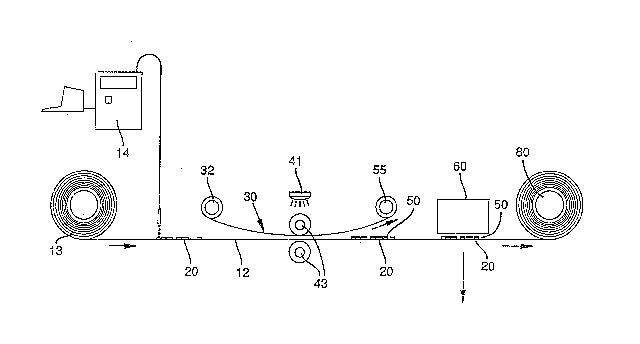
Brie~ ~escriPtion of the ~rawinqs
Fig. 1 is a schematic representation o~ the
process steps, materials, and components used to
produce conductive traces on a substrate in accordance
with the invention.
Fig. 2 is cross sectional view of a flexible film
sheet having a metal layer thereon used in connection
with the invention.
Fig. 3 i an enlarged schematic representation
showing the formation of a conductive trace pattern on
a substrat~ using an adhesive-based ink composition.
Detailed Desc~ietion o~_a ~refer~ed Embodiment
The present invsntion involves an improved method
for producing conductive circuit trace~ in a highly
efficient and economical manner. In accordance with
the invention, an ink composition is first used to
form a selected circuit pattern on a substrate. With
reference to Fig. 1, a substrate 12 i3 illustrated. A
wide variety of substrates known in the art may be
used, including thin-film polyester, ABS
(acrylonitrile-butadiene-styrene) plastic, PC
.
,,
; .,
2~64~
-- 4
(polycarbonate) plastic, PVC (polyvinyl chloride~
plastic, and PC/ABS (50:50) blends. Other substrates
may be used, and the invention shall not be limited to
those listed above.
To implement the present invention on a mass-
production scale, it is desirable to dispense the
substrate 12 from a roll 13 (Fig. 1.) althou~h the
substrate 1~ may consist of a single, flat sh~e~ if
desired. As the substrate 12 is delivered from the
roll 13, it moves toward and through a computer
controllable ink jet printing apparatus 14 known in
the art. In a preferrsd embodiment, a thermal ink jet
printing system is u~ed. Typical thermal ink jet
systems include an ink reservoir in fluid
communication with an orif ice plate and resistor
assembly. These types o~ systems are known in the
art, and described in the Hewlstt-Packard Journal, May
1985, Vol. 36, No. 5. In addition, exemplary ink jet
systems with which the invention may be used are
illustrated in U.S. Patents 4,500,895; 4,794,409;
4,791,438; 4,677,447: and 4,490,728. However, the
invention shall not be limited to any particular type
of ink ~et system, and may be implemented using a wide
variety of ~ystems known in the art, including those
listed above.
The ink ~et printing apparatus 14 is designed to
dispense ink in a selected circuit pattern 20 on the
substrate 12 (Figs. 1 and 3.) The geometry of the
circuit pattern 20 may be varied as de~ired, depending
on the ultimate use for which the circuit i9 intended.
In a preferred embodiment, the pattern 20 will have a
thickness of about 0.5 - 2.0 mil (1.0 mil -
preferred~.
The printing apparatus 14 is supplied with a
specially formulated ink composition designed to
adhere to the substrate 1~ in a rapid and secure
,
20146~9
manner. In accordance with the invention, the
composition includes about 5 - 40% by weight adhesive
(30% by weight = preferred), and about 60 - 95% by
weight solvent (70% by weight = preferred.) A
preferred adhesive usable in the invention is a
product manufactured by the Loctite Corporation of
Cleveland, Ohio under the name "Loctite 408." This
material consists of a cyanoacrylate-based compound.
Another adhesive which may be used is manufactured by
Emhart Australia Pty. Ltd. of Yictoria, Australia
under the name "Bostik Super Bond." However, the
present invention shall not be limited to the specific
adhesives described above, and other adhesives known
in the art may be used accordingly. These adhesives
should be non-toxic, non-flammable, have a viscosity
of about 5 - 100 cps, and a surface tension of about
20 - 60 dynes/cm.
A~ previously indicated, the adhesive i5 combined
with one or more solvents. Exemplary solvents include
ethylene glycol phenyl ether, gamma-butyrolactone,
methyl ethyl ketone, water, and mixtures thereof.
Other solvents known in the art may be used, and the
invention shall not be limited to the solvents listed
above. In addition, the solvents may be mixed in a
variety of e~perimentally determined combinations,
depending on the substrate/adhesive involved, as well
as type of ink jet delivery system being used.
A variety of specific ink compositions produced in
accordance with the invention are described below in
the ~ollowing Examples:
~L
COM~QNENT WT
Loctite 408 (adhesive) 30
gamma butyrolactone (solvent) 50
'
.
201~9
methyl ethyl ketone (solvent) 10
ethylene glycol phenyl ether (solvent) 5
water (solvent) 5
100%
~XAMPLE 2
COMPONENT ~ WT ~_
Bostik Super Bond (adhesive) 30
gamma butyrolactone (solvent) 50
methyl ethyl ketone (solvent) 10
ethylene glycol phenyl ether (solvent) 5
water (solvent) 5
. - -
100%
EXAMP~JE 3
COM~ONENT ~ WT
Loctite 408 (adhesive) 40
gamma butyrolactone (solvent) 50
methyl ethyl ketone (solvent) 5
water (solvent) 5
- :
100~
In a preferred embodiment, the ink composition
will have a viscosity of about 5 - 25 cps (10 cps =
optimum), and a surface tension of about 30 - 60
dynes/cm (50 dynes/cm - op~imum.)
Following application of the ink pattern 20 to the
substrate 12, a thin, flexible sheet of metallized
film 30 is applied to the pattern 20. The film 30 is
pre~erably provided in a roll 32, and is more
specifically i}lustrated in Fig. 2. With continued
refersnce to Fig. 2, the film 30 includes a backing
layer 36 about 5.0 mil thic~ ~1 mil = 25.4 mi~rons)
. : ~, ; . .
.
., : ~ ......... ~ ',. . .
. . : . . .
2014~9
prefarably manufactured of a plastic material known in
the art including but not limited to c~llophane or
polyester. Detachably secured to the backing layer
36 by an adhesive (not shown) is a metal layer 40
which is about 2.0 mil thick. The metal layer 40 may
be manufactured from a wide variety o~ metals and
alloys including but not limited to ~old, copper,
silver, aluminum and mixtures thereof. The film 30
and technical details relative thereto are
specifically described in U. S. Patent 3,519,512 which
is incorporated herein by reference. Also, the film
30 is commercially available from Omnicrom Systems
Limited, U.K.
In use, the film 30 is urged downward against the
pattarn 20, with various portions 42 of the metal
layer 40 contacting the pattern 20, as illustrated in
Fig. 3. In a preferred embodiment, this step is
accomplished simultaneously with the application of
heat and pressure to the film 30 and pattern 20. An
infra-red lamp, oven, or other conventional heating
apparatus 41 is used to heat the film 30 to a
temperature of about 20 - 250 degrees C, with a sub-
range of about 50 - 70 degrees C being preferred. In
addition, the film 30 is applied to the pattern 20
using a downward pressure of about 3 - 5 atmospheres
(1 atm - 10 newton~sq. cm.) This pressure is
ganerated using a pinch roller assembly 43 kno~n in
the art or other comparable pressure-generating
device. The temperature and pressure levels described
above enable the adhesive in the ink to securely
engage and affix the portions 42 of the metal layer 40
to the substrata 12. The unaffixed portions 44 of the
metal layer 40 surrounding the portions 42 shown in
Fig. 3 remain detached from the substrate 12.
After the passage of about 3 - 20 seconds, the
film 30 is withdrawn from the substrate 12. The
:' ' .' ,, ''
.
.
2~14649
portions 42 of the metal layer 40 contacting the
pattern 20 tear away from the metal layer 40 and
remain adhered to the substrate 12, thus forming a
metal trace pattern 50 on the substrate 12. The
pattern 50 has a configuration identical with that of
the initial pattern 20. The unaffixed portions 44 of
the metal layer 40 remain attached to the backing
layer 36 of the film 30. In a preferred embodiment,
the remaining film 30 is wound onto a residue roll 55.
The substrate 12 with the completed trace pattern 50
thereon is then cut as desired using a cutter 50 known
in the art to produce individual circuit units 70
suitable ~or use in a wide variety of applications.
In addition, any residual substrate 12 is preferably
fed onto a collection roll 80, as illustrated in Fig.
1.
The present invention represents a highly
efficient method for applying metal trace patterns to
a substrate. It is especially suitable for use in
high-spaed, mass production manufacturing facilities.
In addition, the use of an ink je~ sys~em to apply an
initial pattern to the substrate enables the pattern
to ba appliQd in a highly precise and controlled
manner.
Accordingly, it is anticipated that suitable
modifications may be made to the invention by
individuals skilled in the art which are entîrely
within the scope of the invention. For example, the
chemicals used to prepare the ink composition, as well
as the matsrial~ used to prepare the metallized film
may be selectively varied. Thus, the present
invention shall only be construed in accordance with
the following claims:
; , -: ,
~ .:
.