Note: Descriptions are shown in the official language in which they were submitted.
- 2~1~3~9
RADIO TELEPHONE SUITABLE FOR
PORTABLE AND VEHICLE-MOUNTED USE
BACKGROUND OF THE INVENTION
The present invention relates to a radio apparatus
and, more particularly, to a radio telephone to be
used as a portable or a vehicle-mounted telephone.
A conventional radio telephone is energized by
a battery in portable use and by a vehicle battery
in vehicle-mounted use. In both cases, a DC voltage
is applied to a receiver section through a voltage
stabilizer. The voltage to be applied to the receiver
section is minimized to save the battery power in the
portable use. As a result, in the vehicle-mounted use,
receiver performance such as an intermodulation (IM)
characteristic and reception sensitivity is sacrificed
for the power saving. On the contrary, if the voltage
is increased to improve the receiver performance, the
life of the battery for portable use will be shortened.
SUMMARY OF THE INVENTION
An object of the present invention is, therefore,
to provide a radio telephone suitable for both portable
and vehicle-mounted use.
Another object of the present invention is to
provide a radio telephone capable of saving power in
,-l' ~
- 2 - 2Q14~69
portable use while improving the receiver performance
in vehicle-mounted use.
Yet another object of the present invention
is to provide a radio telephone having an improved
IM characteristic and reception sensitivity in its
vehicle-mounted use.
A further object of the present invention is
to provide a radio telephone consuming less power
in its portable use.
According to the present invention, there is
provided a portable radio telephone comprising, a receiver
section which includes at least an RF amplifier and
a first frequency mixer. The telephone also comprises
a battery which supplies a first voltage to the receiver
section when the telephone is in portable use. When
the telephone is mounted on a vehicle, a vehicle battery
applies a second voltage which is higher than the first
voltage, to the RF amplifier and to the frequency mixer.
By this higher voltage supply, the intermodulation
characteristic and reception sensitivity of the receiver
section can be improved in the vehicle-mounted use.
On the other hand, battery saving can be achieved by
the lower voltage supply in the portable use.
BRIEF DESCRIPTION OF THE DRAWINGS
The above and other object, features and advantages
of the present invention will become more apparent from
_ _ 3 - 2~ 9
the following description referring to the accompanying
drawings, in which:
Fig. 1 is a block diagram showing a radio telephone
embodying the present invention;
Fig. 2 is a block diagram illustrating a power supply
source to be connected to the Fig. 1 telephone;
Fig. 3 shows a graph demonstrating a IM characteristic
and reception sensitivity with respect to a supply voltage
which were obtained from the telephone shown in Fig. l;
and
Fig. 4 is a schematic circuit diagram showing an
RF amplifier and a first frequency mixer in the Fig. 1
telephone.
DETAILED DESCRIPTION OF THE PREFERRED EMBODIMENTS
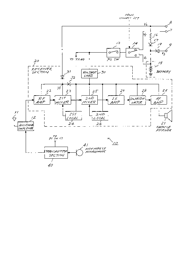
In Fig. 1, a radio telephone 1 includes an antenna 11
picking up a radio frequency (RF) signal and radiating
an RF signal. The picked-up RF signal is supplied to
a receiver section 20 through an antenna duplexer 12.
The receiver section 20, which will be described in
detail later, demodulates the supplied RF signal to
provide an audio frequency (AF) signal to an earpiece
receiver or speaker 21. In response to the AF signal,
the speaker 21 produces an audible signal.
An audible signal which is picked up by a mouthpiece
microphone 41 is supplied to a transmitter section 40
201~9
-- 4
at which the audible signal is subject to modulation and
frequency conversion to become an RF signal. The RF signal
from the transmitter section 40 is transmitted through
the antenna duplexer 12 and antenna 11 to a mobile base
station (not shown), for example. The earpiece receiver 21
and the microphone 41 may be accommodated in the earpiece
and mouthpiece portions of a handset (not shown) of the
telephone 10.
The radio telephone 10 further includes a rechargeable
battery 15 from which a direct current (DC~ voltage V0
is to be supplied through a power supply switch 13 and
a power source switch 14 to both the receiver section 20
and the transmitter section 40. The battery 15 may be
attached to or built in the radio telephone 10. The
power source switch 14 is also connected to a terminal 7
to which a DC voltage Vl is to be applied from a DC/DC
converter 35 connected to a vehicle battery 34 (see
Fig. 2). The switch 14 connects the terminal 7 to the
power supply switch 13 when the radio telephone 10 is
mounted on a vehicle for vehicle-mounted use. On the
other hand, the switch 14 connects the battery 15 to
the power supply switch 13 when the telephone 10 is
removed from the vehicle for portable use. The switch
14 may manually or automatically be controlled. To
achieve the automatic control, a connection detector
may be provided which detects an electrical coupling
2 ~ 9
between the radio telephone 10 and a vehicle battery.
Such a connection detector is disclosed in USP 4,654,882
which is assigned to the same assignee as the present
application and incorporated herein.
When the radio telephone 10 is mounted on a vehicle,
a voltage V2 is applied from the vehicle battery 34
(Fig. 2) to the receiver section 20 though a resistor 38.
The voltage V2 is also applied to the rechargeable
battery 15 through a resistor 16 and a diode 17 in order
to charge the battery 15. The battery 15 is also charged
Dy a DC voltage V3 which is applied through a terminal 9
and a diode 18. The voltage V3 may be obtained from a
commercial alternating current (AC) voltage using an
AC/DC converter 36 to which an AC plug 37 is connected
(see Fig. 2). The voltage V2 is higher than the voltage
V0, Vl and V3 and may be 13.8 volts, for example. The
voltages V0, Vl and V3 may be substantially equal to
each other and V0 and Vl may be 7 volts and V3, 7.7 volts.
The receiver section 20 is a double superheterodyne
type receiver, which is well known in the art and thus
will be briefly described below. The receiver section 20
comprises an RF amplifier 22 for amplifying an RF signal
which is supplied from the antenna 11 through the antenna
duplexer 12. The RF amplifier 22 supplies the amplified
RF signal to a first frequency mixer or connecter 23 to
which a first local oscillation signal is also supplied
- 6 - 2 ~ 1 L~ g ~ ~
from a first local oscillator 24. The first mixer 23
frequency mixes the RF signal and the first local
oscillation signal to produce a first intermediate
frequency (IF) signal.
The first mixer 23 supplies the first IF signal to
a second frequency mixer or connector 25 to which a
second local oscillation signal is also supplied from
a second oscillator 26. The second mixer 25 frequency
mixes the first IF signal and the second local oscillation
signal to produce a second IF signal. The second mixer 25
supplies the second IF signal to an IF amplifier 21 which
amplifies the second IF signal and supplies the amplified
signal to a demodulator 28. The demodulator 28 demodulates
the second IF signal to produce an audio frequency (AF)
signal and supplies the AF signal to an AF amplifier 29.
The amplifier 29 amplifies the AF signal and supplies the
amplified AF signal to the earpiece receiver 21 from which
the AF signal is outputted as an audible signal.
The receiver section 20 further includes a voltage
stabilizer 30 to which one of the voltages V0 and Vl is
applied through the switches 13 and 14. The stabilizer 30
supplies a stabilized voltage of 5 volts, for example, to
the RF amplifier 22 and the first mixer through a diode 32
and to the other elements 24 to 29 directly. To the RF
amplifier 22 and the first mixer 21, the vehicle battery
voltage V2 is to be applied through a diode 31. Thus,
2~3 ~3
when the radio telephone 10 is mounted on a vehicle, the
higher voltage V2 is applied to the RF amplifier 22 and
the first mixer 23. In this case, the lower voltage Vl
is applied to the other elements 24 to 29. When the radio
telephone 10 is demounted from the vehicle for portable
use, the lower battery voltage V0 is applied to all the
receiver section elements 22 to 29.
Fig. 3 shows an IM characteristic with respect to a
voltage Vcc applied to the RF amplifier 22 and the first
mixer 23. Fig. 3 also shows a reception sensitivity (RS)
vs. voltage Vcc characteristic. These characteristics
have been measured using a mack-up set. It can be seen
from the IM vs. voltage Vcc characteristic 51 that as
the voltage Vcc increases, the IM characteristic is
improved. Similarly, it can be seen from the RS vs.
voltage Vcc characteristic 52 that as the voltage Vcc
increases, the reception sensitivity also increases.
Thus, when the higher voltage is applied to the RF
amplifier 22 and the first mixer 23, both the IM and
RS characteristics can be improved.
It should be noted that to improve the IM and RS
characteristics the higher voltage may be applied to
only one of RF amplifier 22 and first mixer 23. In
this case, applying the higher voltage to the first
mixer 23 gives a better result than to the RF amplifier
22.
' s~
-- 8 --
In Fig. 4, the RF amplifier is composed of impedance
matching circuits 221 and 225, a bias circuit 223 and
an NPN transistor 224. The matching circuit 221 includes
a capacitor 101 one of whose ends is connected to a
terminal 226 to which the antenna duplexer 12 is
connected. The other end of capacitor 101 is grounded
through an inductor 103. The junction of the capacitor
101 and the inductor 103 is connected to one end of
capacitor 102 whose other end`is connected to the base
10of transistor 224. The collector of transistor 224 is
connected to the terminal 33 through a resistor 104 of
bias circuit 223. A resistor 105 of bias circuit 223
is connected between the collector and base of transistor
224. The emitter of transistor 224 is grounded.
15The matching circuit 225 includes a capacitor 106
one of whose ends is connected to the collector of
transistor 224. The other end of capacitor 106 is
connected to ground through an inductor 108. The
junction of the capacitor 106 and the inductor 108 is
connected to one end of capacitor 107 whose other end
is connected to the output of RF amplifier 22.
The first mixer 23 is composed of two band-pass
filters (BPFs) 231 and 232, impedance matching circuits
233 and 236, a bias circuit 234 and an NPN transistor 235.
The input of BPF 231 is connected to the output of RF
amplifier 22. The input of BPF 232 is connected to the
- 9 - 2~&1~
output of first local oscillator 24. The outputs of
BPFs 231 and 232 are connected to the matching circuit 233.
The matching circuit 233 includes a capacitor 301 one of
whose ends is connected to the outputs of BPFs 231 and 232.
The other end of capacitor 301 is connected to ground
through an inductor 303. The junction of the capacitor
301 and the inductor 303 is connected to one end of
capacitor 302 whose other end is connected to the base
of transistor 235. The collector of transistor 235 is
connected to the terminal 33 through a resistor 304 of
bias circuit 234. A resistor 305 of bias circuit 234 is
connected between the collector and base of transistor 235.
The matching circuit 236 includes a capacitor 306
one of whose ends is connected to the collector of
transistor 235. The other end of capacitor 306 is
connected to ground through a capacitor 309. The junction
of the capacitors 306 and 309 is connected to one end
of inductor 308 whose other end is grounded through a
capacitor 310. The other end of inductor 308 is also
connected through a capacitor 307 to a terminal 238 which
in turn is connected to the input of second mixer 25.
In operation, an RF signal is applied from the
antenna duplexer 12 to the base of transistor 224 through
the terminal 226 and the matching circuit 221. The
transistor 224 amplifies the RF signal and outputs the
amplified RF signal at its collector. The amplified
lo - 2 ~ 9
RF signal is then supplied to BPF 231 through the matching
circuit 225. Operating and bias voltages are applied to
the collector and base of transistor 224 through the
terminal 33 and the bias circuit 223. As the applied
voltages increase, the IM and RS characteristics are
improved, as shown in Fig. 3.
BPF 231 filters the amplified RF signal to pass and
supply a desired RF signal to the base of transistor 235
through the matching circuit 233. BPF 232 filters the
first local oscillation signal to pass and supply a
desired local oscillation signal to the base of transistor
235 through the matching circuit 233. The transistor 235
frequency mixes the supplied RF and local oscillation
signals with its nonlinear characteristic to provide a
first IF signal at its collector. The first IF signal
is supplied to the second frequency mixer 25 through the
matching circuit 236 and the terminal 238. operating
and bias voltages are applied to the collector and base
of transistor 235 through the terminal 33 and the bias
circuit 234. As the applied voltages increases, the IM
and RS characteristics are improved, as shown in Fig. 3.