Note: Descriptions are shown in the official language in which they were submitted.
2014994
:'
PROTECTED INFORMATION TRANSFER SYSTEM
BACKGROUND OF THE INVENTION
J
Field of the Invention
, ~
This invention relates to systems for transferring
data onto a data bus and reading data from a data bus
and, more particularly, to such information transfer
systems which protect the data bus and prevent the
transfer of erroneous information.
Description of the Prior Art
Typically, information being carried on a data bus
is either read or updated by directly connecting an
add/drop module to the data bus at one of many module
receiving points. In these systems, data is received
("dropped") from the data bus by reading the particular
information directly from the bus through a bus
receiver or amplifier. In order to transmit data or
add data to the bus, a tri-state bus driver is
typically employed at each module receiving location.
In operation, the tri-state bus drivers are
disabled by being placed in a high impedance state
during the time slots when no data is to be transmitted
`T
,. ..
2014994
onto the data bus. In order to control the proper
switching of the tri-state bus drivers, a driver
enable/disable control circuit is required. Whenever
data is to be transmitt~d onto the data bus, the tri-
state bus drivers must be enabled at the precisely
'A desired time slot in order to allow the data from the
add/drop module to be properly transmitted onto the
data bus.
, In using such prior art systems, problems are
j typically encountered primarily due to the need for tri-
state bus drivers. These problems include: timing
problems resulting from the requirement that only one
tri-state bus driver be enabled at any one time; a
relatively high failure rate of tri-state bus drivers;
', and corruption of the data on the data bus often -
occurring due to the requisite connection and
disconnection of add/drop modules to the data bus.
Before the add/drop module can add or transmit
data onto the data bus, the particular tri-state bus
driver must be enabled. This timing is critical, if
the tri-state bus driver is to be capable of adding
data to the data bus during a precisely timed time
slot. In addition, care must be exercised to assure
, that only one tri-state bus driver is enabled at any ~ -
one time, since allowing more than one tri-state bus
., .
.l
~ ",
2014994
driver to be enabled si~ultaneously can damage the tri-
state bus drivers and can cause data errors.
In order to prevent more than one tri-state bus
driver from being enabled at any one time, these prior
art systems are operated with a sufficient timing
margin between time slots, in order to assure that all
tri-state bus drivers achieve the high impedance state
before any other tri-state bus driver is enabled in -
order to allow data transmission onto the bus.
In addition to these drawbacks, these prior art
systems also suffer from the inability of preventing
corruption of the data on the data bus caused by bus
driver failure. When a tri-state bus driver fails, the
failure mode is often a short circuit to a voltage
supply rail which results in the corruption of data on
the data bus. Furthermore, a failure in the tri-state
bus driver enable circuit when an add/drop module is
present can corrupt the data by allowing data from the
add/drop module to be transmitted onto the data bus
continuously.
A further problem inherent in these prior art
systems is the inability of the add/drop module to be
connected or disconnected to the data bus without
guaranteeing that the data will not be corrupted.
Often, transient conditions caused by connecting or
,~
1 ' '
.~ .
201~9~4
disconnecting the additional load to the data bus will
cause the signal level on the data bus to change.
These changes in the signal level can be larqe enough
to be interpreted as data, thereby resulting in data
- corruption. It is essential that the tri-state bus
driver be disabled when the add/drop module is being
connected to the bus.
SUMMARY OF THE INVENTION
It is a principal object of the present invention
to provide an information transfer system, for adding
or reading data to or from a data bus, which protects
the data bus from being corrupted.
Another object of the present invention is to
provide a protected information transfer system which
eliminates dependency upon the timing of a tri-state
bus driver enable circuit.
, Another object of the present invention is to
provide a protected information transfer system which
is not sensitive to failure of tri-state bus drivers or
the enable circuitry associated therewith.
A further object of the present invention is to
, provide a protected information transfer system for
data buses which eliminates the sensitivity of the data
;
. I .
; ~ .
2014994
. 65993-184
~:`
bus to the connection or disconnection of add/drop module~.
-~ Another object of the present invention is to provide a
protected information transfer Rystem for data buses which com-
pletely eliminates the need for tri-state bus drivers to attain
the desired data transfer~
~ The present invention achieves the above objects and
'-3, overcome~ the prior art shortcoming~ by providing one or more
add/drop interface circuitq, each of which is connected in 3eries
with a data bus and is constructed for interconnection with an
add/drop module. Furthermore, each add/drop interface incorpora-
tes control means for selecting the data to be outputted from the
interface and for assuring that the output data has the proper
timing. In addition, any data added to the data bus is also
monitored and added in the precisely desired time slot.
~ In summary, the invention provides an information
i transfer system, adapted for use with add/drop modules for read-
ing data from a data bus and/or adding data to a data bus, 3aid
~y~tem including at least one add~drop interface connected in
series with the data bus and constructed for connection to an
add/drop module, said interface compri~ing:
a data input for connection to the data bus;
a data output for connection to the data bus;
means for connecting to an add/drop module, said mean~ -
including a module output connected to the data input for provi-
ding data from the data bus to the add/drop module, a module
;';'
,.
,'
- 5 -
,
:"
:1
r
~ . ?
201~994
65993-184
input for receiving data from the add/drop module, and signal
means for receiving a module preqent signal from the add/drop
: module;
multiplexing means having a first input connected to
the data input for receiving data from the data bu~ and a second
- input connected to the m~dule input for receiving data from the
add/drop module, said multiplexing means béing responsive to an
output control signal for selecting the data on one of qaid first
and ~econd inputs, and for tran~mitting said ~elected data to the
data output for transmiqæion on the data bus; and
control means connected to the mean~ for connecting to
~ an add/drop module for receiving the module present signal there-
-~ from and for providing said output control signal to said multi-
plexing means in response to said module present signal, whereby
said multiplexing means tran~mits the data received from the
add/drop module when a module is present, and tran~mit~ the data
received from the data bus when an add/drop module i8 not
:~ present.
The add/drop interface of a preferred embodiment of the
~1 20 pre~ent invention al~o includes a filter mean~ which delays
¦ connection of an add/drop module to the data bus to prevent any
transient conditions from affecting the data bus. In this way,
1 transient conditions often caused by the connection of dis-
1 connection of any add/drop module are prevented from affecting
the data bus.
.j . .'. .
`"
.: - 5a - :
1 .
201~994
DESCRIPTION OF THE DRAWINGS
For a fuller understanding of the nature and
objects of the present invention, reference should be
made to the following detailed description taken in
connection with the iaccompanying drawings in which:
Figure 1 is a circuit diagram showing the
conventional prior art construction for transferring
information to and from a data bus;
Figure 2 is a circuit diagram showing the
protected information transfer system of the present
invention; and
Figure 3 is a detailed circuit block diagram
showing the add/drop interface employed in the
protected information transfer system of the present
invention,
,~ :
DETAILED DESCRIPTION OF THE PREFERRED EMBODIMENT
In order to best understand the unique advantages
attained by the protected information transfer system
of the present invention, a conventional prior art
~ system is shown in Figure 1. As shown therein, a
;, single add/drop module 21 is directly connected to a
data bus 20 through a bus receiver 22 and a tri-state
I -6- :
,.~ , .
,~. ~ . .
~ ~ ,
201~994
bus driver 23. Bus receiver 22 communicates with the
add/drop module 21 connected thereto to read
information from the data bus when activated. Tri-
state bus driver 23 is used to transfer information
from add/drop module 21 to data bus 20, when enabled.
In order to prevent information from being
erroneously added to data bus 20 from add/drop module
21, this prior art system requires a tri-state bus
driver enable/disable circuit 24, which is connected
between add/drop module 21 and tri-state bus driver
23. When the tri-state bus driver is to be disabled,
the enable/disable circuit places tri-state bus driver
23 in a high impedance state, thereby isolating the
module from the data bus and preventing information
from being transmitted from module 21 to data bus 20.
When information is to be added from module 21 to
data bus 20, tri-state bus driver enable/disable
circuit 24 must enable tri-state bus driver 23 during a
precisely desired time in order to iassure that the
information is transferred from module 21 to a precise
time slot on data bus 20. In addition, at the precise
time the information has been fully transferred,
enable/disable circuit 24 must disable tri-state bus
driver 23 by returning the bus driver to its high
impedance state.
-7- -
'. :~
~: '
2014994
As is apparent to one of ordinary skill in the
art, the prior art system shown in Figure 1 represents
one connection of a plurality of connections used to
add and read information from a typical data bus.
Consequently, as detailed above, the difficulty
typically encountered with such prior art systems is
substantial due to the plurality of tri-state bus
drivers being employed and the fact that the timing of
each of these tri-state bus drivers must be carefully
controlled. Consequently, inherent restrictions are
imposed on the system, rendering the entire information
transfer system susceptible to all of the difficulties
- and drawbacks detailed above.
' By employing the present invention, all of the
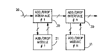
j prior art problems resulting from the use of tri-state3 bus drivers are completely eliminated. As shown in
Figure 2, the present invention eliminates the need for
tri-state bus drivers by connecting an add/drop
~ interface 30 directly in series with data bus 20 for
j each add/drop module connection point desired. Each
add/drop module 21 is connected directly to an add/drop
` interface 30. In this way, the protected information
transfer system of the present invention is attained.
' ~, .'
'l ~
-~ :
. .
,
2014994
In order to provide the desired protected
information transfer system, each add/drop interface
incorporates the necessary circuitry to protect the
data bus 20 at each connection point for an add/drop
module 21. Each add/drop interface 30 comprises the
requisite circuitry to eliminate the need for tri-state
drivers, thereby providing data bus 20 with protection
from driver failure. The circuitry also prevents
connections or disconnections of modules to or from the
data bus from corrupting the data on the bus.
In order to best understand the operation of
add/drop interface 30 of this invention, reference
should be made to Figure 3, wherein the circuit
construction of add/drop interface 30 is shown in
detail. By referring to Figure 3 along with the
following detailed disclosure, the operation and
construction of the protected information transfer ~-
system of the present invention can best be understood.
Add/drop interface 30 of the present invention
incorporates three principal components, a multiplexer
controller 31, a data multiplexer 32 and a delay flip- -
flop 33. In addition, add/drop interface 30 also
incorporates a line receiver 36, a line driver 37, and
a retiming flip-flop 38.
.
2014~4
In the preferred embodiment, add/drop interface 30
is connected in series with the data bus with an input
25 from the data bus to interface 30 being connected to
lines 40, 41 and 42 of interface 30. Line 40
represents a through data path, since it carries the
data from the data bus through delay flip-flop 33 to
data multiplexer 32. Line 41 transmits data to
multiplexer controller 31, via line 48, while
controller 31 drives data multiplexer 32 by
transmitting control signals along line 45.
Preferably, the clock signal from the data bus is
separated from line 41 and is transmitted on line 50
directly to an interface output 47 which is connected
to the data bus. The same clock signal is also
transmitted on line 51 to retiming flip-flop 38. In
this way, interface 30 assures that the information
transmitted as the output to the data bus has the
proper timlng.
In order to add information to or read information
from the data bus, an add/drop module is connected to
line driver 37 and line receiver 36. In addition,
whenever an add/drop module is connected to interface
30, a module present signal is delivered from add/drop
module 21 to multiplexer controller 31 on line 39. In
this way, any information to be read by the add/drop
,''~
:-`
:
, ~ i "~.,",~,," ",~, ,,,",,,,,,",, " ,~, ",", ,,,,"~, ,;" ~ ,, ";,,, ~ ",
2014994
module is transmitted on line 42, through line receiver
36 to the add/drop module on line 52, while any
information to be added to the data bus is transmitted
from the add/drop module to line driver 37 on line 53,
and then to retiming flip-flop 38 on line 54.
As clearly shown in Figure 3, data multiplexer 32
receives two inputs, one from delay flip-flop 33 on
line 40, which represents the through data path. The
second input is from retiming flip-flop 38 on line 46,
which represents the add/drop data path.
The function performed by data multiplexer 32 is
to select which data path, the through data or the
add/drop data, is to be presented to the output 47 of
the add/drop interface 30 or delivery to the data
bus. This path selection by the data multiplexer 32 is
controlled by the multiplexer controller 31, based upon
the several factors detailed below.
Delay flip-flop 33 provides the necessary delay in
the through data path to equalize the delay in the
add/drop data path to within one data clock period. As -~
a result, this delay insures that the phase of the
frames arriving at both inputs to data multiplexer 32 -
are the same.
' ~;Z
~ ~ -11- ~ .,
l .-,
."1 ,
2014994
In addition to cont:rolling data multiplexer 32,
multiplexer controller 31 provides error monitoring in
order to protect against failures. This error
monitoring is performed by comparing an error checking
data pattern which is carried on the data bus at both
the input 25 and output 47 of the add/drop interface.
In order to provide this error checking, multiplexer
controller 31 monitors the data bus input along lines
41 and 48, while monitoring the output to the data bus
on line 49. The specific error checking data pattern
to be used is not important as long as the pattern is
present and the timing of the pattern is known to the
multiplexer controller 31.
In operation, multiplexer controller 31 checks the
pattern received on line 48 from the data bus input 25
with the pattern received on line 49 from the data bus
output 47. If the error checking pattern does not
match, an error is declared. In addition, an error
flag is set based upon a predetermined number of errors
declared. Multiplexer controller 31 incorporates an
instruction set which establishes the predetermined
number based upon the type of data being transported on
the bus.
. 5
.j :
1 -12-
. , .
,...
'1
:, .
201~994
Another feature provided by the information
transfer system of this invention is the incorporation
of means in multiplexer controller 31 to assure that
the data being transmitted on the data bus is not
corrupted by transients created by the connection or
disconnection of the add/drop module. In the preferred
embodiment, when the add/drop module is connected and
the module present signal changes from NOT SET to SET,
the module present signal transmitted to multiplexer
controller 31 is filtered or delayed for eight frames
before multiplexer controller 31 sets the module
present flag. In this way, transient conditions caused
by the connection of the add/drop module are dissipated
before the data multiplexer 32 connects the add/drop
data path to the data bus. In the case of
disconnection of the add/drop module, the multiplexer
controller 31 can be provisioned prior to disconnection
so that the data multiplexer 32 switches to the through
data before the module is disconnected.
In operation, multiplexer controller 31 normally
drives the data multiplexer 32 to select and transmit
the through data being received on line 40. In this
way, the data being received by add/drop interface 30
from the data bus is transmitted through delay
flip/flop 33 to data multiplexer 32 and then to output
-13-
201A994
47 from data multiplexer 32 for transmission to the
data bus as the output of add/drop interface 30.
Alternatively, multiplexer controller 31 drives
data multiplexer 32 to select the add/drop data path,
being received by data multiplexer 32 on line 46, when
a signal is received by multiplexer controller 31 on
line 39, representing a module present signal, and the
module present flag has been set without any error flag
being set. When these conditions are met, data
multiplexer 32 receives the data from line 46
representing the add/drop data path and delivers the
data to output 47 of add/drop interface 30.
As discussed above, retiming flip-flop 38 is
employed to assure that the data transmitted to line 46
has the proper timing for delivery to the data bus. To
assure maintenance of this timing, line 51 delivers the
clock signal from the data bus to retiming flip-flop
38, thereby assuring that the output of flip-flop 38 is
properly timed.
Although the add/drop interface of the present
invention can be employed in a variety of data bus
applications, the present invention is directly
applicable to add/drop multiplexers used in
telecommunications networks. In particular,
telecommunication signals typically employ a time
-14-
20149g4
division multiplex frame format, such as SONET OC-N.
These signals can easily be transmitted on the
protected add/drop data bus o~ the present invention.
In particular, the framing pattern incorporated into
these signals is easily used as the error checking
pattern, and a frame strobe signal derived from the
framing pattern is easily employed to identify the
framing pattern. Furthermore, the serial bit stream of
the tele~ommunications signal could be easily converted
to a parallel format in the interface.
By employing the add/drop interface of the present
invention, the data bus is protected against failure,
as well as beinq protected against data corruption
often occurring when an add/drop module is connected or
disconnected to the data bus. In addition, the present ~
invention allows add/drop multiplexers to be - -
constructed with an internal data bus having access to
all of the information content of the time division
multiplex frame at all points along the data bus. In
this way, interfaced systems having varying and mixed
information bandwidths can be connected to the data
bus.
It will thus be seen that the objects set forth
above, and those made apparent from the preceding
description, are efficiently attained and, since
-15-
65993-184 20~4994
cartain changes may be made in the above circuit
without departing from the scope of the invention, it
is intended that all matter contained in the above
description or shown in the accompanying drawings shall
be interpreted as illustrative and not in a limiting
sense.
It is also to be understood that the following
claims are intended to cover all of the generic and
specific features of the invention herein described and
all statements of the scope of the invention, which as
a matter of language, might be said to fall
therebetween.