Note: Descriptions are shown in the official language in which they were submitted.
`` 2~15~11
Optical communication technology includes wavelength
multiplexing techniques which can transmit optical signals with
a plurality of different wavelengths simultaneously and allot
different information to different wavelengths in order to
effectively utilize transmission path. This type of technique
needs optical receivers with a function which enables the
separation of optical signals according to their wavelengths.
The present invention relates to an optical receiver of this
type. More particularly, the present invention relates to an
optical receiver which has a function of separating multiplex
optical signals according to their wavelengths when the
spectrum of the wavelengths of the optical signals is narrow
and stable.
Fig. 1 is a schematic view which illustrates an
example of a conventional optical receiver;
Fig. 2 is a schematic view which illustrates another -
example of a conventional optical receiver;
Fig. 3 is a graph showing output characteristics of
the example of the conventional optical receiver shown in
Fig. 2;
Figs. 4 through 11 are to explain a first embodiment
of an optical receiver of the present invention, in which:
.~ "~
~' -'.
- 1 - . -.
` ~01~211
Fig. 4 is a schematic perspective view illustrating
the configuration of the optical receiver according to the
first embodiment of the present invention;
Figs. 5A and 5B each are a first diagram showing an
example of optical power distribution in an optical multimode
circuit for explaining the first embodiment of the present
invention;
Figs. 6A, 6B, 6C and 6D each are a second diagram
showing another example of optical power distribution in an
optical multimode circuit for explaining the first embodiment
of the present invention;
Figs. 7A, 7B, 7C and 7D each are a graph showing - ~.
optical power distribution of an optical multimode waveguide at .
its output terminal surface, which is intended to explain the
wavelength resolution of the optical multimode waveguide used :
as the optical multimode circuit in the first embodiment of the :~
present invention; . -
Figs. 8A, 8B and 8C each are a graph showing ~ ~
experimental results illustrating the operation of an optical ~ ~ -
receiver according to the first embodiment of the present ::-
invention, in which:
Fig. 8A is a graph showing a transmission waveform
pattern at an optical input portion;
, ! --2
''il~ ~ .'.''-.
',, . ,.'.
*/ ,'~ ''`'~ ,' ' ' "' . "',."`'''' ' .j';' ," , ' ' . . ' ' ' '
2û1~211
Fig. 8B is a graph showing a waveform pattern at a
photo-detector array;
Fig. 8C is a graph showing a waveform pattern of
branched light at an output side of a neural network;
Fig. 9 is a schematic perspective view of the optical -
receiver according to the first embodiment of the present
invention in which heterodyne detection mechanism is included;
Fig. 10 is a diagram showing an example of the neural
network having a self learning function;
Fig. 11 is a timing chart showing the action of the ~ -
neural network shown in Fig. 10;
Fig. 12 is a schematic perspective view of an optical
receiver according to the second embodiment of the present
invention;
Fig. 13 is a schematic perspective view of an optical
receiver according to the third embodiment of the present
invention;
Figs. 14 through 17A, 17B, 17C and 17D each are to
explain an optical receiver according to the fourth embodiment - -
of the present invention, in which:
i~ A
. .:
2015211
Fig. 14 is a schematic perspective view of the optical
receiver according to the fourth embodiment of the present
invention;
Fig. 15 is a schematic perspective view of a hologram
element, illustrating a mechanism for memorizing patterns in
the hologram element;
Figs. 16A and 16B each are a diagram exemplifying
optical power distribution at terminal surface for each
wavelength of output light from the optical multimode circuit
used in the fourth embodiment of the present invention~
Figs. 17A, 17B, 17C and 17D each are a diagram
exemplifying optical power distribution at terminal surface of -~
wavelength multiplexed optical signals of output light from the
optical multimode circuit used in the fourth embodiment of the
present invention;
.
Fig. 18 is a schematic perspective view of the
configuration of an optical receiver according to the fifth
embodiment of the present invention;
. .
Fig. 19 is a plan view of the configuration of an
optical receiver according to the sixth embodiment of the
present invention; ~
, ..'
. - ~ . .
, ~ ~ 4 ~ -
''.'.'' ~ '
2al1521~
Fig. 20 is a plan view of the configuration of an
optical receiver according to the seventh embodiment of the
present invention;
Fig. 21 is a plan view of the configuration of an
optical receiver according to the eighth embodiment of the
present invention;
Figs. 22 _hrough 26 each are to e~plain the ninth
embodiment of the present invention, in which:
Fig. 22 is a plan view of the configuration of an
optical receiver according to the ninth embodiment of the - --
present invention;
Fig. 23 is a graph showing optical power distribution -
on a photo-detector array;
Fig. 24 is a graph showing distribution of
photocurrent when signal light with a wavelength Al is
received by the photo-detector array;
Fig. 25 is a graph showing distribution of --
photocurrent when signal light with a wavelength ~ 2 is
received by the photo-detector array; and
,. ~ .
~; A ~
201 ~211
Fig. 26 is a graph showing distribution of
photocurrent when signal light with a wavelength A n is
received by the photo-detector array.
Fig. 1 sh~ws an example of a conventional optical
receiver. As shown in Fig. 1, wavelength-multiplexed signal
beam 1 is scattered by an angle scatter element 3 after being
transmitted through an optical fiber 2 and transmitted light
rays are detected by respective photodetectors 4-1 to 4-5 which
receive corresponding light rays scattered at respective
scatter angles. In Fig. 1, reference numerals 5 and 6 indicate
an incident side lens 5 and an outgoing side lens 6. As will -
be clear Çrom the above-described configuration, the
conventional optical receiver is a device constructed so as to ~-
detect differences in angle in terms of differences in
position. Therefore, with the optical receiver, smaller
differences in scatter angle give rise to smaller differences
in position, which makes detection of differences difficult
accordingly. Generally, allowadce in the difference in
position is small, e.g., as small as several tens micrometers :
(~m), when the optical receiver is used to divide
wavelength-multiplexed light of which distance between adjacent -
wavelengths is in the order of 10 nm, and for this reason high
accuracy on the order of micrometers ~m) is required for
optical coupling the angle scatter element 3 with the
photodetector 4. This increases production costs of the device. -~
~v ',,'' ':
._^~ ,,
;l'.`'' ' :','.. ',' ,',' .'.'' ~'i'; ' 'i ' , ' ';, ' '', '' ' ' '.~' `; I :' ' ' '
20i~21~
In additi~n, it is natural ~hat the conventional
optical receiver deteriorates its demultiplexing
characteristics even with a slight fluctuation in the
wavelength of light source because it requires high precision
on the order of micrometers in the optical coupling of the
angle scatter element with the photodetector.
As will also be clear from the configuration shown in
Fig. 1, the variation of the wavelength of the light source
results in difference in the scatter angle for signal light,
which requires for alterations in the design of the device.
Therefore, the optical receiver lacks sufficient flexibility in
its response toward changes in conditions such as fluctuation
in wavelength.
As described above, the conventional optical receiver
is disadvantageous in that it is uneconomical since its
production cost is high and it haæ poor demultiplexing
characteristics as well as it has poor flexibility towards -
various conditions upon measurement. ;
As another example of conventional optical receivers -
there is known a device which has a configuration as shown in
Fig. 2. Thiæ type of optical receiver includeæ a combination
of an optical receiver with an optical demultiplexer which
realizes Mach-Zehnder interferometer that has been well known ;
in the field of classical optics using optical waveguides. ;~-
1- A ~ :
~ .
2~1~211
In Fig. 2, symbols 7A through 7F indicate single mode
optical waveguides, 8A and 8B directiunal couplers, 9A through
9D ports, and lOA and lOB optical elements. The two
directional couplers 8A and 8B are connected to each other via
the two single mode optical waveguides 7A and 7B. The optical
circuit shown in Fig. 2 has four ports 9A, 9B, 9C and 9D. The
two single mode optical waveguides are different from each
other in their length. Therefore, considering the case where
optical signals are launched into the port 9A, the optical
signals which have been separated with the directional coupler
8A and transmitted separately through the single mode optical
waveguides 7A and 7B, respectively, are synthesized again in
the directional coupler 8B, the optical signal which has been
transmitted through the single mode optical waveguide 7A has a
phase different from that of the optical signal which has been
transmitted through the single mode optical waveguide 7B. The
phase difference varies depending on the wavelength (or
frequency) of the optical signals. The outputs from the ports
9C and 9D are determined depending on the phase difference.
Fig. 3 shows output characteristics obtained at the
ports 9C and 9D, e.g., in the case where the separation ratio
is 1 : 1 assuming that the wavelengths (or frequencies) of the
two optical signals launched into the port 9A are fl and
f2, respectively. In this case, the optical output at the
port 9C is high and that at the port 9D is low at the
wavelength fl and on the contrary the optical output at the
port 9C is low and that at the port 9D is high at the
201~211
wavelength f2. Utilizing these characteristics, the device
can be used as an optical demultiplexer which allows signals
fl and f2 launched into the port 9A to branch and be
outputted from the ports 9C and 9D, respectively. Therefore,
in the conventional optical receiver described above, in order
to separate individual signals according to respective
wavelengths from wavelength multiplexed optical signal, it has
been so designed that photodetectors 10A and 10B are connected
to the output ports 9C and 9D, respectively, so that electric
signals OA and OB obtained from the respective photodetectors
can be utilized as they are. That is, the electric signals OA
and OB have been utilized as electric signals which correspond -
to optical signals with wavelengths (or frequencies) fl and
f2, respectively~
However, in the case where optical receivers are to be
realized with the conventional configuration as shown in
Fig. 2, subtle difference in the length and position of the
optical waveguides gives a great influence on the wavelength
separation characteristics of the devices since they utilize
interference between the optical waveguides. For this reason,
there has been required high technique for designing and
producing optical circuits, and if such technique were
available the temperature of the optical circuits produced must
be controlled with a precision of less than 1/10 C and thus
their characteristics tend to vary absent such temperature
control. Further problem is that the configuration of the
optical circuit becomes more complex with increased number of
A
~ .................... ' ~ .
2~1~211
the wavelengths to be used, which causes increase in the scale
of the circuit and deterioration of loss characteristics.
An object of the present invention is to provide an
optical receiver which can separate a plurality of optical
signals with different wavelengths in wavelength multiplexed
optical communication in which a light source with a narrow and
stable wavelength spectrum, using an optical circuit which is
simple and easy to fabricate.
'. . ' ' .
To attain the above-described object, the present -
invention provides an optical receiver comprising two elements,
i.e., an optical conversion device tA] for converting
difference in wavelength to difference in spatial power
distribution and pattern recognition means for recognizing the
pattern of the spatial power distribution and taking out output
signals.
:
. ~
The optical conversion device [A] as the first element
of the optical receiver of the present invention may be
classified roughly into two groups, i.e., an optical multimode ~
circuit (1) and a diffraction grating ~2). The optical ~ -
multimode circuit (1) is composed of only an optical multimode
waveguide tl]; an optical circuit 12] is composed of an optical
multimode waveguide and a plurality of optical waveguides
connected to an output terminal of the optical multimode
waveguide; and an optical circuit [3] is composed of a
201521 i
combination of a plurality of optical waveguides, a directional
coupler and Y-branch devices.
Therefore, specific examples of the optical conversion
device as the first element [A] of the optical receiver of the
present invention includes the following four types of devices: ~-
(i) an optical multimode waveguide [1] alone;
(ii) an optical circuit [2] composed of an optical
multimode waveguide and a plurality of optical
waveguides connected to an output terminal thereof;
(iii) an optical circuit [3] composed of a combination of a
plurality of optical waveguides, directional couplers
and Y-branch devices; and
(iv) a diffraction grating.
The term "optical waveguide" referred to herein also
includes optical ibers. - ~-
. .
Examples of the pattern recognition means as the
second element ~B] of the optical receiver of the present -
invention include the following three types of devices: ;~
~i) a configuration comprising a photo-detector array
which receives optical signals on optical power
distribution from an optical conversion device and
converts the signals into electric signals, and a
neural network which comprises a plurality of
processing elements and connection elements and
processes the electric signals from the photo-detector
A - 11 - `
, . .
, : .
.. . ~
2~15211
array and takes out output signals that correspond to
individual light signals with respective wavelengths
contained in the multiplex or single wavelength light
signals which are launched into the optical conversion
device; -
(ii) a configuration comprising a hologram element which
receives the optical signals launched from an optical
conversion device, processes the optical signals
according to their wavefront conditions and produces
output lights having optical power distributions which
correspond to individual light signals with respective
wavelengths contained in the multiplex or single
wavelength light signals launched into the optical
conversion device, and a photo-detector array which
receives the output signals from the hologram element ;
and converts the optical power distributions thereof
into electric signals; and :~.
(iii) a configuration comprising the above-described
hologram element, photo-detector array and neural
network.
The neural network is preferably the one which has a
self-learning function.
The present invention will bs described in detail with
reference to attached drawings illustrating preferred
embodiments which are shown by way of example and it should not
be construed that the present invention is limited thereto.
- 12 - :~
,,,, .', ;'::
2~15~11
The first embodiment of the present invention is
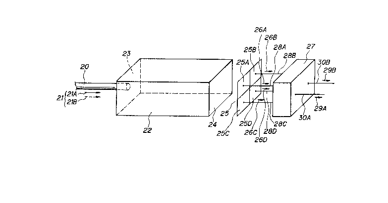
shown in Fig. 4, in which reference numeral 20 is an
optical input portion, 21A and 21B optical signals, 22 a
optical multimode circuit (herein, optical multimode
waveguide alone~, 23 one terminal surface (input terminal
surface) of the optical multimode circuit 22, 24 the other
terminal surface (output terminal surface) of the optical
multimode circuit 22, 25A through 25D photo-detector ~-
arrays, 26A throughout 26D electric signals, 27 a neural
network, 28A through 28D input ports, 29A and 29B output
signals, and 30A and 30B output ports.
As described above, this embodiment is characterized
~y a configuration in which the optical multimode circuit
is connected to the photo-detector arrays and the neural
network in order to separate individual signals contained
in the respective optical signals with different
wavelengths. Therefore, definite difference between this
embodiment and the prior art is in that the former uses an
optical multimode circuit and a neural network. The term
"neural network" as used herein refers to a signal `-
processing network which comprises processing elements
realized by an addition processor in which weighted
addltion of signals from a plurality of input ports are ~;- -
performed and a non-linear processor in which input
signals are processed non-linearly, and connection ~
elements which combine the processing elements with each ~ ;
other, i.e., an optical circuit which has functions of
- 13
,. ~,
~ " ~ " ,,:~"~ .". .;
201521~
recognition, association, learning and the like of input
signals launched into the whole network. For this type of
technology, reference is made, for example, to D. E.
~rr e/harz ~ce/e//~/7d
Rumme~Lb~K~, J.L.~McEll~nd and the PDP Research Group:
"Parallel Distributed Processing~, MIT Press, Cambridge
(1986).
Next, explanation will be made on the operation of
the optical receiver having the above-described
configuration. The optical signal 21 launched into the ~ -
optical input portion 20 contains optical signals 21A and
21B with wavelengths different from each other. After ~
coming out of the waveguide of the input portion 20,the -
optical signals 21A and 21B propagate in the optical
multimode circuit 22 and come out of one terminal surface
24 thereof and enters the photo-detector array 25 and are
combined therein. It should be noted that the
configuration shown in Fig. ~, the optical multimode
circuit 22 is constructed by only a optical multimode
waveguide. In the photo-detector array 25, the
photodetectors 25A, 25B, 25C and 25D convert optical
signals into electric signals 26A, 26B, 26C and 26D,
respectively. The electric signals 26A, 26B, 26C and 26D
enter the neural network 27 from the input ports 28A, 28B,
28C and 28D, respectively, and are processed therein. As
the result, final output signals 29A and 29B are obtained
from the output ports 30A and 30B.
In the embodiment of the configuration shown in Fig.
4, the optical power distribution of the optical multimode
- 14 -
2015~11
circuit 22 on its output side terminal surface varies
depending on difference in the wavelength of the optical
signal 21. This is because a plurality of modes which are
propagatéd in the optical multimode circuit 22 have
propagation constants different from each other in
wavelength dependence and thus there naturally occurs
wavelength dependence in the optical power distribution on
the output side terminal surface 2~ which appears as the
result of interference among the respective modes. The
optical power distribution of a type which appears on a
terminal surface of a optical multimode circuit when light
having a narrow spectrum is propagated in the optical
multimode circuit is generally called as "speckle pattern"
as described in R. E. Epworth: "Modal Noise - Causes and
Cures", Laser Focus, pp. 109-115 (Sept. 1981). Although
the incident optical system on the input side terminal
surface 23 of the optical multimode circuit 22 is
stationary as shown in Fig. 4, difference in the
wavelength of the optical signal 21 gives rise to
different optical power distribution on the output side -
terminal surface 24.
Figs. 5A and 5B show examples of optical power -
distribution on the output side terminal surface 24. Fig.
SA shows optical power distribution when only the optical
signal 21A is launched into the optical multimode circuit
22 while fig. 5B shows optical power distribution when -
only the optical signal 21B is launched into the optical
. ' ' -
- 15 -
''' ' ' ~
' :"
201~211
multimode circuit 22. ~he slashed area indicates optical
power higher than that indicated ~y blank area.
Assume that two optical signals 21A and 21B are
modulated with respect to their intensity with digital
signals bearing different information to form wavelength
multiplexed optical signals which then are introduced into
the optical multimode circuit 22 via the optical waveguide
of the input portion 20. Then, the optical signals can be
in one of four states:
(1) a state in which the optical signals 21A and 21B are
"1" and "0", respectively;
(2) a state in which the optical signals 21A and 21B are
"0" and "1", respectively;
(3) a state in which the both optical signals 21A and 21B
are "1"; and
(9) a state in which the both optical signals 21A and 21B
are "0".
Figs. 6A, 6B, 6C and 6D each show optical power
distribution in the case of the above-described state (l),
(2), (3) or (4) based on the examples shown in Figs. 5A
and 5B. Black area indicates optical power higher than ;
that indicated by slashed area and the slashed area has -
optical power which is between optical power of blank area
and the black area.
As will be apparent from Fig. 6, the optical power -
distribution on the output side terminal surface 24 varies
for each of the four states described above. The four -
optical power distribution patterns shown in Fig. 6A, 6B,
- 16 - :
',. ,
20~5211
6C and 6D, respectively, are detected with the photo-
detector array 25 and the respective electric signals 26
are launched into the neural network 27. The neural
network 27 has a function that enables presetting of its
internal conditions so that corresponding predetermined
output patterns can be generated when predetermined input
signal patterns are introduced. Assuming that the two
output signals 29A and 29B from the neural network 27 have
signal levels El and E2, respectively, the internal
conditions of the neural network 27 can be set up such
that E1 = l and E2 = O when the optical power distribution
is the one shown in Fig. 6A, El = O and E2 = 1 when the
optical power distribution is the one shown in Fig. 6B, E1 - --- -
= 1 and E2 = 1 when the optical power distribution is the
one shown in Fig. 6C, or E1 = O and E2 = O when the --
optical power distribution is the one shown in Fig. 6D.
Figs. 7A through 7D are graphs elucidating by
simulation the extent of variation in pattern caused by -
the optical multimode circuit (actually, optical multimode
waveguide alone). As for the optical multimode circuit
including a core and a clad, a two-dimensional slab form - -
guide which is of multiple mode in the x-direction is
taken as an example. Assuming that there occurs no
penetration of electromagnetic field into the clad the
distribution of electromagnetic field of the n-th mode is
expressed in a scalar amount as follows~
En = sin ~nx/a) (1)
where a indicates the width of the core. ~ -~
- 17 -
,... .
20~211
It is assumed that the core has a refractive index of
1.46, NA and the width of the core are 0.2 and 22.5 ~m,
respectively. These values correspond to the case where
the highest mode number is 6. The length of the guide is
set up to 10 cm. What is connected to the photo-detector
array is near field pattern of a optical multimode
waveguide.
Calculation is performed assuming that six modes
represented by the equation (1) above are excited
uniformly on the input side terminal surface of the
optical multimode waveguide. Fig. 7 shows optical power
distribution on the output side terminal surface when the
wavelength of the optical signal increases by 1 nm ~-
starting fr~m 1,550 nm. From this it follows that in -
order for clear change to be observed in the optical power
distribution, it is necessary and sufficient that there -~
occurs change in wavelength on the order of 1 nm. The
extent of this wavelength dependence is proportional to --
second power of the length and NA of the optical multimode
circuit. -
Furthermore, in order to demonstrate realizability of
the optical receiver according to this embodiment,
experiments have been performed using the same
configuration shown in Fig. 4 except that two photo-
detector arrays and two input/two output type neural
network are used to carry out demultiplexation at a rate
of two wavelength/100 Mbit/s. The results obtained are
shown in Figs. 8A through 8C.
- 18 -
.
20~ 5~11
-Fig. 8A shows the transmitted waveforms for signals
of ~1 (upper trace) and ~2 (lower trace) including four
states~ 2) = (0, 0), (0, 1), (1, 0) or (1,1). The
detected waveforms at the two PD's are shown in Fig. 8B.
The optical signals for ~1 and ~2 are superimposed in each
waveform according to the optical power distribution. The
neural network correctly regenerates the original signals
as shown in Fig. 8C~
From this it follows that even if optical signals 21A ~
and 21B which have different wavelengths and have been - -
modulated with respect to their intensity with different
signals are received at the optical input portion 20 in
Fig. 4 in a wavelength multiplexed state, the original
modulation signals can be regenerated at the output ports
20A and 30B of the neural network 27 in accordance with
the embodiment shown in Fig. 4.
In the above description, an example was taken for
simplicity which used intensity modulated optical signals.
However, the present invention is applicable not only to ~
such intensity modulated cases but also to frequency ~ -
modulated cases. In the case of intensity modulation, the
optical power distributions A-l and A-2 shown in Figs. SA ~
and 5B, respectively, appear or disappear on the terminal ~ -
suxface corresponding to the states of "1" or "0" of the
optical signals 21A and 21B having different wavelengths.
On the other hand, in the case of frequency modulation, -
the optical power distribution assumes two patterns ~-
corresponding to the state "1" or "0" of the optical
- 19 - ',~'.'
2~152t 1
signal 21A. Therefore, there ~ppear four different
patterns for two wavelength multiplexed signal light.
This is because the intensity of light is constant and
only the frequency assumes two values in the case of
digital frequency modulation and therefore there appear
optical power distributions corresponding to the
respective frequencies on the output side terminal surface
24. If the internal conditions of the neural network 27
are set up taking into consideration the four patterns,
the original modulation signals can be regenerated
similarly to the case of intensity modulation. Here, -~
bivalent digital frequency modulation has been explained.
However, the same idea is of course valid for multivalent
digital frequency modulation. -
In the foregoing, although the first embodiment of
the present invention has been explained with reference to
Figs. 4, 5A and 5B, 6A through 6D, 7A through 7D and 8A
through 8C, the configuration of the optical receiver of
the present invention should not be construed as being :
limited to the one shown in Fig. 4 or to those described
in the following embodiments but obviously there may be
made various variations thereon as described, for example,
in (1) to (10) below.
That is, in the first embodiment of the present
invention the following measures may be taken.
(1) In the above description, the number of the optical -~-
signals with different wavelengths is 2, that of the
elements of the photo-detector array 25 is 4, that of the
- 20 -
2 ~
input ports 28 of the neural network 27 is 4, that of the
output ports 30 of the neural network 27 is 2, and that of
the output signals is 2. However, these numbers may be
set up freely depending on the purpose.
(2) Although it has a shape of a three-dimensional optical
waveguide, the optical multimode circuit 22 may be a two-
dimensional optical waveguide in the form of a slab.
~imilarly, the photo-detector array 25 can be made a one-
dimensional array instead of the two-dimensional array.
(3) The optical parts or optical circuits are connected to -
each other directly or through space. However, it is -
possible to arrange a lens system or systems so as to
intervene therebetween at a desired position or positions. ~-
(4) The photo-detector array 25 detects optical power
distribution on the output ~ide terminal surface 24 as it
is. More particularly, near field pattern of the optical --
power on the terminal surface 24 is detected by the photo- -- -
detector array 25. In contrast, the output side terminal ; ~-
surface 24 and the photo-detector array 25 may be
connected to each other in a spatially remote state. In
this case, far field pattern of optical power on the - -
output side terminal surface 24 is detected by the photo- ~;
detector array 25. The far field pattern, like the near
field pattern, varies in accordance with difference in the
wavelength of the optical signal 21. Therefore, processed -
signal output similar to that in the case of the near
field pattern described above can be obtained by
.
- 21 - :
. . -
2~152~1
introducing the electric signal 26 from the photo-detector
array 25 into the neural network 27.
(5) There are two types of input signal light 21 obtained
by wavelength multiplexing signal light which has been
digitally modulated for its intensity. One is a type in
which the wavelengths are synchronized with each other and
the other is a type in which the wavelengths are not in
synchronization. In the present invention, both of them
are applicable. However, in synchronized systems, timing
pulses must be inputted for achieving synchronization for
the non-linear processor in the neural network. Of
course, the synchronized systems can operate at higher
maximum speeds.
~6) The optical multimode circuit 22 may be a small size -
optical circuit, for example, the one which can be placed
in one apparatus or a long optical multimode fiber of, for
example, several tens kilometers long. In the latter
case, the left hand side terminal of the device shown in
Fig. 4 corresponds to the transmission side of the optical
transmission system and the right hand side thereof ~
corresponds to the receiver side of the optical - ;-
transmission system.
~7) The optical input portion 20 is used for introducing
the optical signal 21 into the optical multimode circuit
22. Of course, the optical input portion 22 may be an
optical space beam in place of the optical waveguide as
shown in Fig. 4.
' . ',
- 22 - ~
'' ..', '' '
2~211
(8) Although the photo-detector array 25 and the neural
network 27 are connected to each other directly,
electronic circuits such as amplifiers may be inserted
therebetween, if desired.
(9) Although optical signals containing a plurality of
wavelengths are introduced into the optical multimode
circuit, the same processing as shown in Fig. 4 is
possible when optical signals is of single wavelength if
the wavelength varies continuously or discontinuously with
lapse of time. In this case, the optical power
distribution on the output side terminal surface 24 varies -
according as the wavelength varies, which makes it
possible to detect the variation in wavelength as output ~-
from the neural network 27.
~10) The photo-detector array 25 directly detects the
optical power distribution on the output side terminal ~ -
surface 24 of the optical multimode circuit 22. On the
other hand, in the field of optical communication, there
are in addition to such direct detection technique as ~ - `
described above so-called heterodyne detection technique
or homodyne detection technique in which light from a
local transmission light source provided on the
transmission side is mixed with the optical signal
received before detection can be performed (cf., e.g., -
Shimada: "Coherent Optical Communication", Electronic
information Communication Association, (1988)). The
features of the detection techniques are in that the
influence of thermal noises in the photodetector can be ~ ;
' " '
- 23 - ~
' ' ' .
20~21~
suppressed to thereby improve the sensitivity of
photodetection. In the present invention, the heterodyne
or homodyne detection technique may be adopted.
Fig. 9 exemplifies a configuration of the optical
receiver in the above-described case. In Fig. 9, a part
indicated by reference numeral 31 newly added to the
configuration shown in Fig. 4 is an optical waveguide for
introducing light from the local transmission light source
provided on the receiver side into the optical multimode -
circuit 22. In Fig. 4, the optical waveguide 16 is
connected directly onto the input slde terminal surface 23
of the optical multimode circuit 22. To perform
heterodyne detection, i.e., to detect the received
optical signals (from the optical input portion 20) after -~ -
mixing them with the light from the local transmission ~ -
light source provided on the transmission side (from the -
optical waveguide 31), it is necessary to conduct pre-
mixing sufficiently. Therefore, although there may also
be employed without particular disadvantages a
configuration in which the optical waveguide 16 is
connected directly to the input side terminal surface 23 -~
of the optical multimode circuit 22 as shown in Fig. 9, it
is preferred to use another configuration in which the -
optical waveguide 31 is connected to the optical input
portion 20 on the upstream of the optical multimode
circuit 22.
Although no description has been made hereinbefore,
the neural network 27 may be a hardware composed of one or
-- 2 4 --
.',: .
,:
2~1~211
more electronic or optical circuits, or it may be a
computer which has input and output terminals and is
controlled by a software.
As described above, the neural network 27 is a signal
processing network constructed by a plurality of addition
processor which performs weighted addition of signals from
a plurality of input ports and a plurality of connection
elements which connect non-linear processors to each other
for the input signals, and it is an optical circuit which
has functions of recognition, association, learning and
the like of input signals into the whole network. In the
present invention, it is preferred that the circuit has a
learning function. -
Fig. 10 exemplifies a configuration of an optical -
receiver with such neural network (NN) having a learning
function and Fig. 11 shows a timing chart relative to the
operation thereof. In the case where the neural network -
has a learning function, a learning circuit 40 and a
pattern generator 41 are added as parts of the neural
network 27. The learning circuit 40 renews weight (W) and
threshold value ~)of the neural network 27 in accordance
with the contents of advanced learning. The pattern
generator 41 also generates teacher signals.
Learning operation is as follows. Firstly, the light
source repeatedly launches 24 = 16 patterns as indicated
by ~1 to ~4 shown in Fig. 11. The optical signals are ;
converted into electric signals by the photo-detector
array 25 and then subjected to pattern recognition by the
.
- 25 -
, .:
201~211
neural network 27 to be outputted as signals Dj (j = 1,2,
3 or 9). Since they are subjected to S-form mild
recognition processing, the signals show analog-type
amplitudes. Learning proceeds by comparing the amplitude
of the output signals Oj with that of the teacher signals
tj, and gradually renewing the internal conditions
(weight: Wij, threshold value: ~i) of the neural network
so that the state function E = ~(tj - oj)2 can be minimum.
Upon the comparison, the pattern in which the teacher
signals ti are generated must coincide with the pattern of
signals launched from the light source. For example, the
light source side signals assume fourteenth signal pattern
shown in Fig. 11, learning becomes nonsense unless the
teacher signals are of the same pattern as the fourteenth
pattern shown in Fig. 11. However, it is not always the
case that the patterns coincide with each other when the
launching of the signals is initiated. In Fig. 11, the
teacher signal pattern is eleventh pattern when the light
source side signal pattern is the fourteenth one.
Therefore, there is a need for the synchronization of --
patterns. Pattern synchronization can be realized by
resetting the pattern generator with a reset signal as --
shown in Fig. 10. Generation of reset signals is realized
by NAND gate in the configuration of this embodiment. -
When the signal of the fourteenth pattern is introduced -
into the NAND gate, a reset signal is generated and the
pattern generator begins to produce output starting from O
~zero)-th pattern. As for the input signal to be
- 26 -
201~21 1
introduced into the NAND gate, there can be used signals
O~ which are obtained by recognizing and regenerating the
output signals Oj from the neural network by a recognizer
with a timing clock. Delay due to the light source signal
occurs in regenerated signals OTj, and the amount of delay
in the example shown in Fig. 11 amounts to one time slot
equivalent. - -
After pattern synchronization is achieved, learning
for 16 patterns are performed in a plurality of times, and
the learning circuit sends a learning end signal as soon
as the value of the state function E becomes smaller than ~`
a predetermined value to terminate the learning. -
Fig. 12 illustrates the second embodiment of the ~ -
present invention. The same reference numerals or symbols
are used for the same parts or members as those used in
the first embodiment shown in Fig. 4. Major difference
between the second embodiment shown in Fig. 12 and the
first embodiment shown in Fig. ~ is in that the optical
multimode circuit have different configurations from each -
other. In the first embodiment, ~i) only the optical
multimode waveguide is used while in the second embodiment
there iS used (ii~ an optical circuit constructed by an
optical multimode waveguide and a plurality of optical
waveguides connected to its output side terminal. In this :
embodiment, the number of the optical waveguide is 4. The
four optical waveguides are provided on their output side
- 27 -
:'
2~1~211
terminal with the photo-detector array 25 composed of four
elements 25A through 25D.
Fig. 13 illustrates the third embodiment of the
present invention. The same reference numerals or symbols
are used for the same parts or members as those used in
the first embodiment shown in Fig. 4. Major difference
between the second embodiment shown in Fig. 13 and the
first embodiment shown in Fig. 4 is also in difference in
the configuration of the optical multimode circuit used. -
In the third embodiment, there is used as the optical
multimode circuit an optical circuit constructed by (iii)
a combination of a plurality of optical waveguides,
directional couplers and Y-branch devices. In this
embodiment, the number of the optical waveguide is 4.
Many types of optical circuits can be realized by changing
the combination. Needless to say, the conventional
optical demultiplexer shown as an example of the prlor art
may be included as a part of the optical circuit described
above.
,~ .
Fig. 14 illustrates the fourth embodiment of the
present invention. The same reference numerals or symbols
are used for the same parts or members as those used in
the first embodiment shown in Fig. 9. Major difference
between the fourth embodiment shown in Fig. 14 and the
'-
- 28 -
2~1~2~1
first embodiment shown in Fig. q is in that the pattern
recognition means for recognizing spatial power
distribution is different between the two embodiments. In
the first embodiment, the means is (i) the photo-detector --
array and the neural network while in this embodiment
pattern recognition is performed by (ii) a hologram
element and a photo-detector array.
The output light from the optical multimode circuit
22 is connected to the hologram element. In a hologram
element 71, the output light 70 from the optical multimode
circuit is processed depending on the wavefront conditions
thereof with the information stored in the hologram
element 71 to form output light 72 different from the
output light 70. ~he output light 72 from the hologram -
element is connected to a photo-detector array 73 and :
converted into electric signals. As the result, final
output signals 75A and 75B can be obtained from output
ports 74A and 74B, respectively,of the photodetector 73. -
The hologram element 71 must store or memorize output
pattern 76 from the optical multimode circuit 22 before it -
can operate. For memorization, reference light or wave 77 -~
is used as shown in Fig. 15 in the same manner as in the ~ -
conventional technique to cause interference with signal
light or wave bearing information on the output pattern 76
and the holoqram element is sensitized ~ith the resulting
.
lnterfered pattern. The reference light 77 is irradiated
in the direction at an angle of ~ with respect to the
. . . .
direction in which the output pattern 76 is propagated. ~ ~
~ '
- 29 - ~
. ~ '
2015211
The angle ~ varies depending on the wavelength of the
reference light.
When it is irradiated to the memorized hologram
element 71, the output pattern 76 is diffracted in the
direction of the reference light 77. Therefore, there
arise diffraction waves in directions corresponding the
respective wavelengths, which makes it possible to perform -
wavelength separation. When a spherical wave which is
propagated from a point source of light is used as the
reference wave, diffracted wave becomes a beam which is
focusing on the position of the point source of light, and
therefore wavelength separation is facilitated by
arranging a photo-detector array 73 at the very position
of focusing. In the case where a broad parallel beam is
used as the reference wave, diffracted wave is also a ~-
broad beam which distributes on the photo-detector array ~
73. In the latter case, a neural network is arranged` -
downstream of the photo-detector array in the manner
described hereinbelow in order to perform recognition
processing.
In the embodiment shown in Fig. 14 which has the -
configuration as described above, like the first
embodiment described above, the optical power distribution
appearing on the output side terminal surface 24 of the
optical multimode circuit 22 is different between the case
where only the optical signal 21A having a predetermined
wavelen~th iS launched into the optical multimode circuit
22 and the case where only the optical signal 21B having
. .. ..
. ....
- 30 -
,
~",~,"",,,."""`',,.,.,,",~;,':~ '' ''''"j"''''' " '~'': ~"~
201~211
another predetermined wavelength is launched thereinto.
For example, the optical power distribution shown in Fig.
16A is outputted for the optical signal 21A having first
wavelength while the optical power distribution shown in
Fig. 16B is outputted corresponding to the optical signal
21B having second waveleng~th, and in this manner input
optical signal with different wavelength gives rise to
output optical power distribution of different pattern.
Likewise, when the two optical signals 21A and 21B are
subjected to intensity modulation with respective -
different digital signals and the resulting wavelength -
multiplexed signals are launched into the optical -
multimode circuit 22 via the input optical waveguide 20, -~
the optical signals received may be in one of four states.
'~he optical power distributions on the output side ~ -
terminal surface 29 for the four states are as shown in
Figs. 17A, 17B, 17C and 17D, respectively. The four
distribution patterns are launched into a hologram element -
71. Also in the hologram element 71, like the case where
the neural network 27 described in the first embodiment, -
it is possible to set up the internal conditions thereof
so that hologram output light 72 corresponding to one of
the optical power distribution shown in Fig. 17A -
throughout 17D based on the signal levels of two output
signals 75A and 7SB from a photo-detector array 73.
From the above it follows that even when the optical -
signals 21A and 21B which have different wavelengths and
have been modulated for their intensities with different
- 31 -
201~211
signals are received in the input optical waveguide 20
shown in Fig. 19 in a wavelength multiplexed state, it is
possible according to the embodiment shown in Fig. 11 to
regenerate the original modulation signals also in output
ports 74A and 74B of the photo-detector array 73.
In the foregoing, the case where intensity modulated
optical signals have been exemplified as in the preceding
embodiments in order to simplify the explanation. -
However, the present invention is applicable not only to
the case where intensity modulation is used but also to
the case where frequency modulation is adopted. Likewise, -~
the same idea is no doubt applicable to the case where -
multivalent digital frequency modulation is performed
although description has been made herein on the case of
using binary digital frequency modulation.
Although explanation has been made on the fourth
embodiment as described above, the present invention is
not limited to the configuration shown in Fig. 14 or scope
shown in various embodiments referred to hereinafter but
various variations may be made which are similar to the
variations (1) to (10) described above with respect to the
first embodiment. In this case, care must be taken on -
various modifications in the configuration such as
replacement of the neural network by the hologram element.
Though not described earlier, the hologram element 71
may be the one in which information is stored on a two-
dimensional plate or the one in which information is
. .
., :
- 32 -
201~211
stored three-dimensionally using three-dimensional optical
crystals.
Fig. 18 illustrates the fifth embodiment of the
present invention. The same reference numerals or symbols -
are used for the same parts or members as those used in ;-
the fourth embodiment shown in Fig. 14. Major difference
between the fifth embodiment shown in Fig. 18 and the
fourth embodiment shown in Fig. 14 is in that the optical
multimode circuit 50 which has a new configuration is
provided in the fifth embodiment in place of the optical -
multimode circuit 22 used in the fourth embodiment. The
optical multimode circuit 2~ is a single optical multimode
waveguide while the optical multimode circuit 50 in the
fif~h embodiment is constructed by a-plurality of optical
waveguides (four optical waveguides in this embodiment). -~
In other words, the optical multimode waveguide 51 and the -
four optical waveguides 53 connected to the terminal
surfaces 52 of the optical multimode waveguide function
togéther as the optical multimode circuit 50. This
configuration is similar to that of the optical receiver
according to the second embodiment shown in Fig. 12. The
photo-detector array 73 is connected to the four optical
waveguldes 53 via the hologram element 71.
. ':
.
- 33 -
, - ~
.
2~1~2~1
Fig. l9 illustrates the sixth embodiment of the
present invention. ~he same reference numerals or symbols
are used for the same parts or members as those used in
the third and fourth embodiments shown in Figs. 13 and 14,
respectively. Major difference between the sixth
embodiment shown in Fig. 19 and the fourth embodiment
shown in Fig. 19 is, like in the case of the fifth
embodiment, in that the optical multimode circuit 60 which
has a new configuration is provided in this embodiment in
place of the optical multimode circuit 22 used in the
fourth embodiment. The optical multimode circuit 22 is a
single optical multimode waveguide while the optical
multimode circuit 60 in the fifth embodiment is
constructed by a plurality of optical waveguides. In -
other words, a combination of a plurality of the optical ~ -
waveguides 54 and the optical branching circuit 55 and the
directional coupler 56 connected to each other functions
as the optical multimode circuit 60 in this embodiment.
This configuration is similar t~ that of the optical
receiver according to the third embodiment shown in Fig.
13. In this configuration, many types of optical circuits
can be constructed by changing the combination and
connection of the optical waveguides 54. Of course, the
optical demultiplexer constructed by a single mode optical
waveguide as illustrated in Fig. 2 as an example of
conventional optical demultiplexer is also included in the
.'' " ," -,',
_ 34 ~
20~,21 1
optical receiver accordlng to the present invention as a --
part thereof.
Fig. 20 illustrates the seventh embodiment of the
present invention. In this embodiment, a polarization
separation element 80 is inserted between the optical ~
multimode circuit 22 and the hologram elements 71A and -
71B. After the output light 70 from the optical multimode
circuit 22 is separated into polarized light rays 70A and
70B, the respective polarized light rays 70A and 70B are
connected to the two hologram elements 71A and 71B.
Output light rays 72A and 7?B from the hologram elements ~
71A and 71B, respectively, are connec~ed two photo- --
detector arrays 73A and 73B arranged downstream thereof,
and output signals from the photo-detector arrays 73A and
73B are added and outputted by an addition circuit 81.
Usually, the optical signal 21 launched into the optical
waveguide 20 assumes various polarized states and for this -
reason an optical receiver having polarization independent
optical demultiplexing characteristics can be realized by
adopting the configuration as shown in Fig. 20.
Fig. 21 shows the eighth embodiment of the present
invention. In this embodiment, the neural network 27
described in the first embodiment above is connected at
the downstream of the photo-detector array 73. Utilizing
~ ~ '
- 35 - ~
:, ;'
2~15~1~
the pattern recognition function which the neural network
27 has, this embodiment enables further improvement in its
signal regeneration characteristics.
Fig. 22 shows the ninth embodiment of the present
invention. In Fig. 22, reference numeral 90 indicates a
diffxaction grating, 91 a one-dimensional photodetector
(PD) array arranged linearly, and 27 and 30 are a neural
network and an output port thereof as in the preceding
embodiments. -
Major difference between this embodiment and other -
preceding embodiments is in the use of the optical
conversion device 90.
As shown in Fig. 22, the wavelength multiplexed
signal light 21 is scattered angularly or diffracted by
the diffraction grating 90 to form an angularly scattered
signal light 92 . Here, the wavelength multiplexed signal `
light 21 is a digital signal modified with respect to its
intensity. On the photo-detector array the angularly
scattered (diffracted) signal light 92 is converted into -
an optical power distribution having a single peak per -- -~
wavelength as shown in Fig. 23. As will be apparent from ~
Fig. 23, the optical power distribution varies ~ i
continuously in the direction in which the array is
arranged. However, since the photodetector has a limited
size, the distribution of photoelectric current is ~;
represented by discontinuous or stepwise patterns as shown -
, ~:
- 36 - ~ ~
: ~' , ' -
.-',', .-:. :~
2~15~1 1
in Figs. 29 through 26. When the plural si~nal light rays
are in a state of ~ON~ simultaneously, the distribution of
photoelectric current is linear addition of the respective
photoelectric currents thereof. Pattern recognition
processing by the neural network 27 of such photoelectric
current distribution outputted from the photo-detector
array 91 results in the regeneration of signals
corresponding to the respective wavelengths from the
output ports 30 of the neural network 27.
As stated earlier, the internal conditions of the
neural network 27 can be set up electrically so that it
can generate specified output patterns in accordance with
specified input patterns based on its function. For
example, it can be set up such that a pattern [1, 0, .....
0] is outputted form the output port 30 [l, 2, -----,
n] in response to an input of electric current
distribution as shown in Fig. 29. The number of patterns
to be preset is 2n when the number of wavelength
multiplexing is n assuming that binary signals are used.
In this case, there occurs no deterioration of
demultiplexing characteristics according accompanied by
variation in wavelength since the neural network (N~) -
automatically alters the internal conditions thereof to
ad~ust the demultiplexing wavelength even if vaxiation in
wavelength occurs in the light source. ~
In Figs. 24 through 26, the number of the -- `
photodetector (M) and that of multiplexed wavelengths (n)
must satisfy the following relationship: n ~ M.
- 37 -
2~15~11
As described above, in this embodiment, optical
connection with high precision is unnecessary since the
optical receiver is designed so that optical power
distribution is received by the whole photo-detector
array.
Although this embodiment uses a diffraction element --
is used as angular scattering element, the same operation
can be performed when a prism is replaced therefor. .
'.
. ,. `~,
:. '. ~,
, ~
~;; '
''. ,''''~, ~': '
- 38 - ~
.
'~ ''.,',','''''',-.'"' .