Note: Descriptions are shown in the official language in which they were submitted.
IM~GE RE~DING APPARAlTtlS
BACKGROVND OF THE INVENTION
1 l. Field of the Invention
The present invention relates to automatic gain control
of an image reading apparatus using a line image sensor.
BRIEF DESCRIPTION OF THE DRAWINGS
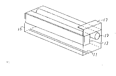
Fig. l is a schematic perspective view showing an
embodiment of the reading unit of the image reading apparatus
according to the present invention;
Figs. 2 and 3 are schematic perspective views showing
examples of arrangement of the same embodiment of the reading
apparatus according to the present invention;
Fig. 4 is a schematic Derspective view showing the
conventional image reading apparatus;
Fig. 5 i5 a block connection diagram showing the
automatic gain control circuit in the conventional image
reading apparatus; and
Figs. 6 and 7 are diagrams showing signal waveforms at
various portions of the automatic gain control circuit of Fig.
5 for explaining the operation of the circuit.
1 2. Description of Prior Art
Fig. 4 is a schematic perspective view showing the
conventional image reading apparatus as disclosed, for example,
in Japanese Patent Unexamined Publication No. Sho-63-316567.
In the drawing, the reference numeral 11 designates a line
image sensor having a multi~row structure for reading a picture
signal; 12, a light source; 13, a rod lens array; 14, an
original; and 15, a white reference plate attached on the
apparatus body at a position adjacent to the original 14.
Here, as the line image sensor 11, used is one long
enough in length to read the original 14 as well as the white
reference plate 15 at the same time.
Fig. 5 shows an automatic gain control circuit in the
conventional image reading apparatus. In the drawing, the
reference numeral 11 designates a line image sensor; ~1 and
22, amplifiers; 23 and 24, analog-to-digital converters
(hereinafter, referred to as A/D converters); 25 and 26, sample
hold circuits; and 27 and 28, amplifiers.
The line image sensor 11 is constituted by an image
sensor having a two-row structure in which one row is
constituted by white (W) elements and yellow (Ye) elements
arranged alternately in this order and the other row is
- constituted by green (G) elements and cyan (Cy) elements
arranged~alternately in this orderl so that a picture signal
is produced from the two rows. One picture element is
constituted by the four adjacent W, Ye, G, and Cy elements.
Next, the operation of the conventional image reading
ap~aratus will be described.
l First, an image of the oriyinal 14 and the white
reference plate 15 irradiated by the light source 12 is focused
on the line image sensor 11 through the rod lens array 13 in
Fig. 4. In Fig. 5, the picture signal put out from the one
row of the line image sensor 11 constituted by the W and Ye
elements is applied to the amplifier 21 so.as to be amplified
therein and the picture signal put out from the other row of
the line image sensor 11 constituted by the G and Cy elements
is applied to the amplifier 22 so as to be amplified therein.
The output S(l) of the amplifier 21 is applied to the
A/D converter 23. As for the picture signal of the white
reference platel the picture signal put out only from the W
elements is sample-held by the sample hold circuit 25 so as to
be utilized as a reference voltage Ref(1) of the A/D converter
23.
The output S(2) of the amplifier 22 flows similarly to
the picture signal S~1). In the case of the picture signal
S(2), however, the picture signal put out only from the G
elements is sample-held by the sample hold circuit 26.
Fig. 6 shows signal waveforms at main portions of Fig.
5. In Fig. 6, S(l) represents a one-line picture signal which
is applied to the A/D converter 23 when scanning is performed
in the direction of line starting from the white reference
plate 15 side; S/H represents a pulse signal which is only the
sample-held picture signal put out from the W elements
corresponding to the white reference plate; and ref (1)
represents a reference voltage applied to the A/D converter 23.
1 Further, the level of the picture signal S(1) is lower in the
vicinity of the opposite ends than the center portion in one
line because of a shading effect of the light source 12 as
shown in Fig.`6.
The reference voltage ref (1) to be applied to the A/D
converter 23 is obtained by amplifying the output of the sample
hold circuit 25 by means of the amplifier 27, as shown in Fig.
5, with a suitable amplification factor (for example, with an
amplification factor ~i ~Ai>l) ) to thereby make correction so
that a one-line picture signal is with~n the range of A/D
conversion.
In the foregoing configuration, even in the case whére
the intensity of light of the light source 12 so fluctuates in
sub-scanning that the picture signal changes, for example, from
S~1) shown in Fig. 7 (a) to S'(1) shown in Fig. 7(b), the
reference voltage ref (1) applied for every line to the A/D
converter 23 changes at the same rate as that of the picture
signal if the white reference is read before reading every
line.
That is, the following expression is established.
ref'(l) = ref(l)*(S'(1)/S(l))
Therefore, the output of the A/D converter 23 is even
reyardless of fluctuations of the intensity of light.
Although description has been made as to the method of
automatically controlling the gain of the picture signal S(l)
in reference to Fig. 6 and Fig. 7(a), (b), quite the same
applies to the output S(2) of the amplifier 22 as for the
~i.
l operation thereof except that in this case the picture signal
from the G elements is sample-held by the sample hold circuit
26 so as to be used as the reference voltage for the A/D
c~nverter 24.
S Thus, the reference voltages ref (1) and ref (2) are
obtained from the picture signals produced from the W and G
elements respectively and the white reference is read by the
A/D converters 23 and 24 in accordance with the reference
voltages ref (l) and ref (2) respectively. Therefore, reading
of the white reference is accurate in comparison with the c~se
of a single system, and each of the outputs of the A/D
con~erters 23 and 24 is even regardless of the fluctuations of
the intensity of light.
Having such a configuration as described above, the
conventional image reading apparatus has a problem in that if
a part of the white reference plate 15 becomes dirty or dust
sticks on a part of the white reference plate 15, the reading
level of the white reference plate 15 falls only in the dirty
portion so that the signal level for one line based on the
reduced reading level relatively rises to thereby cause local
disturbance, such as transversal stripes having higher
luminance than other portions, in an output picture.
-- 5 --
SU~RY OF TH:E _I NVENT I ON
The present invention has been accomplished to solve
the above problem, and is intended to pxovide an image reading
apparatus in which even if- a part of a white reference plate
becomes dirty or dust sticks on a part of the white reference
plate, no local disturbance, such as transversal stripes, is
caused in an output picture.
The image reading apparatus according to the present
invention comprises a reading unit constituted by an integrally
provided optical system formed of a line image sensor, a rod
lens array, a light source, and the like, and a white reference
plate attached on one end of the reading unit.
According to the present invention, since the white
reference plate moves together with the reading unit in
direction of sub-scanning in reading an original, one and the
same portion of the white reference plate is read for every
line so that no variation due to dirt or dust is caused in
reading level. Accordingly, it is possible to prevent
deterioration, such as generation of transversal stripes, from
occurring in the output picture.
, .
2 ~ 2 ~
- DETAI~ED DESCRIPTION OF PREFERRED EMBODIMENTS
An embodiment of the present invention will be
described hereunder with reference to the accompanying
drawings. Fig. 1 is a schematic perspective view showing an
s embodiment of the reading unit according to the present
invention. In Fig. 1, constituent components the same as or
corresponding to those of Fig. 4 are correspondingly
referenced, and duplicate explanation is omitted. In Fig. 1,
the reference numeral 16 designates a reading unit for scanning
o (s-ub-scanning) an original 14 in reading the original. The
reading unit 1~ has an optical system composed of a line image
sensor 11, a light source 12, a rod lens array 13, and the like
which are arranged so as to he able to perform integral
scanning. The reference numeral 17 designates a white
reference plate attached on one end of the reading unit 16 so
as to be moved together with the reading unit 16 in the
sub-scanning direction. The white reference plate 17 is
attached on the reading unit 16 in a manner so that the white
reference surface is located in the same plane on which the
original 14 is mounted as shown in Fig. 2. Alternatively, the
white reference plate 17 is attached on the reading unit 16 in
a manner so that the white reference surface is located just
under a glass plate 18 on which the original 14 is mounted as
shown in Fig. 3.
2 ~ 2 ~
A circuit for processing a picture signal produced from
the line image sensor 11 has the same configuration as that of
the conventional image reading apparatus.
Next, the operation will be described.
~irst, the original 14 and the white reference plate
17 attached on the one end of the reading unit 16 are
irradiated with the light source 12 arranged in the reading
unit 16 so that the respective images of the original 14 and
the white reference plate 17 are focused on the line image
o sensor 11 through the rod lens array 13. A circuit for
processing a picture signal produced from the line image sensor
ll has the same configuration as that of the conventional image
reading apparatus.
Being attached on the reading unit 16, the white
S reference plate 17 is interlocked with the light source 12,
the rod lens array 13, and the line image sensor 11 so that
one and the same portion of the white reference plate 17 is
read for every line.
Even if a part of the white reference plate 17 becomes
dirty, therefore, the reading level of the white reference
plate 17 referred to when the signal level of the original 14
is determined for every line falls at the same rate for all the
lines, so that the white reference does not become different
among the lines. Consequently, the signal level in reading the
2s original relative to the reading level of the white reference
2~1~426
-plate never becomes .different .among the lines even if the
intensity of light of the light source fluctuates, 80 that an
original read.ing signal having a level which is not different
among the lines can be obtained after A/D conversion.
s Accordingly, deterioration in picture quality, such as loca~
generation of transversal stripes, can be prevented to thereby
make it possible to obtain an output which is even in ~uality
over the whole surface of the original 14.
~ lthough description has been made as to the case of
lo reading a color image in the above embodiment, the present
invention provides the same effects as those obtained in the
above embodiment also in the case of performing reading by
means of a monochrome sensor in which no color separation
filter is provided on the .line image sensor il.
15Further, in the above embodiment, the white reference
plate 17 is attached to the reading unit 16 in a manner so that
the white reference plate 17 is located on the right of the
original 14 in the drawings as show in in Figs. 2 and 3. Thus,
it is made possible that the reading unit 16 reads the white
reference plate 17 before performing scanning from the right to
the left for every line to thereby produce a reference voltage
for every line so that the reading of each line can be
performed on the basis of the thus obtained reference voltage.
Alternatively, in the case where the fluctuation of the
intensity of light of the light source 12 is sufficiently
2 ~
gentle relative to the time required for one-line reading of
the line image sensor 11, the configuration may be made changed
such that the white reference plate 17 is attached on the
reading unit 16 so that the white reference plate 17 comes on
the left of the original 14 and the reading unit 16 reads the
white reference plate 17 attached on the left of the original
14 so as to generate a reference voltage after reading for
every line to thereby make it possible that the next line can
be read on the basis of the thus obtained reference voltage.
o - Moreover, although the white reference plate 17 is
attached on the same plane as the original 14 or just under
the glass plate 18 in the above embodiment, the white reference
plate 17 may be attached at any position of the reading unit 16
so long as the white reference plate 17 can be irradiated with
the light source 12 so that the image of the white reference
plate 1~ can be made on the line image sensor 11 through the
rod lens array 13 to thereby make it possible to obtain a
reading signal. Also in this case, the same effects as those
obtained in the above embodiment can be obtained.
As described above, according to the present invention,
the reading unit is constituted by the optical system
integrally provided with the line image sensor, the rod lens
array, the light source, and the like, and the white reference
plate is attached on one end of the reading unit. Therefo~e,
there is an effect in that one and the same portion of the
-- 10 --
2015~2t~
white reference plate is read by the line image sensor every
time an original is read line by line to thereby make it
possible that the gain control can be made on the basis of the
output of the line image sensor. Furthex, even if a part of
s the white reference plate becomes dirty, an even output can be
obtained throughout the whole surface of the original to
thereby make it possible to prevent deterioration, such as
generation of transversal stripes, from occurring in the output
picture.
.