Note: Descriptions are shown in the official language in which they were submitted.
_ 1- 201 5805
ALTERNATOR VOLTAGE TRAN8I~NT MININIZATION
METHOD AND APPARAT~
The present invention relates generally to
electronic voltage regulation of field current in an
alternator which, for example, can form part of a
battery charging system for an automotive vehicle.
More particularly, the invention is directed to a
method and apparatus for using a pair of high voltage
MOS Insulated Gate Bipolar Transistors (MOSIGBT's) to
control the current in a field w;n~ing of such an
alternator to both maintain a desired regulated output
voltage and to protect the alternator and circuitry
connected to the alternator from high voltage
electrical transients generated if the alternator is
disconnected from a load either intentionally or due to
a fault condition. The present invention is
particularly applicable to automotive battery charging
systems and, accordingly will be described with
reference to such a system.
In automotive battery charging systems, voltage
regulation is commonly performed by monitoring an
alternator output voltage/battery voltage and
controlling the current through a field winding of the
alternator to power automotive Ioads and to charge the
battery. If a fault occurs within a charging system,
such as the disconnection of the alternator from the
battery, large transient voltages are generated at the
alternator. The large transient voltages are due to
the energy of self-inductance of the field winding and
can damage the alternator, the regulator and/or other
automotive loads if connected to the alternator output
at the time the fault occurs.
-
2015~o5
88-102 -2-
In the prior art, attempts have been made to
avoid damage by connecting voltage limiting and/or energy
dissipating elements to the alternator output, the field
winding of the alternator or the associated automotive
loads. One example of a prior art attempt at transient
control is illustrated in Murari et al, U. S. Patent No.
4,455,585 wherein integrated circuits manufactured
according to the usual processes for low voltage
integrated circuit structures are employed. In Murari et
al, a zener diode is connected either directly or
switchably in series with a return diode to control a
fault transient such that low voltage structures can be
used. Alternately, the series connected zener diode and
return diode are replaced by a low voltage PNP transistor
which is connected across the field winding. A
conventional regulator is connected to the PNP transistor
base terminal to keep the transistor in the conducting
state to return field current when a field current control
transistor is inoperative and to produce a predetermined
voltage between the collector and the emitter during a
fault condition.
Unfortunately, Murari et al's low voltage PNP
transistor cannot suppress the field decay transient to an
effective level and may shunt the field winding during
normal operation and hence contribute to loss of
alternator regulation. Field winding shunting occurs due
to operation of the low voltage PNP transistor in its
inverse active region as the result of large reverse
voltages which are repeatedly applied across the
collector/emitter terminals of the PNP transistor as the
regulation transistor is switched on and off.
3 20 1 5805
Accordingly, there is a need for a method and
apparatus for controlling the current in a field
winding of an alternator to maintain a desired
regulated alternator ou~u~ voltage and to protect the
alternator and equipment connected to an ou~u~ of the
alternator in the event the alternator is disconnected
from a load it is driving, for example by a fault
within a charging system utilizing the alternator,
which otherwise causes potentially damaging high
voltage transients at the alternator output.
This need is met by the method and apparatus of
the present invention for controlling field current in
an alternator wherein a pair of MOS Insulated Gate
Bipolar Transistors (MOSIGBT's) are connected one in
series and one in parallel with a field win~ing of the
alternator. In this configuration, current is provided
as needed to the alternator field winding through the
series connected transistor to maintain the alternator
output at a desired voltage level and the field current
is returned through the parallel connected transistor
when the series connected transistor is turned off.
When the alternator output is disconnected from a load,
for example, due to a-fault in a battery charging
system including the alternator, both transistors are
switched off in a controlled manner to discharge the
field winding energy at an accelerated rate within the
parallel connected transistor. The series connected
transistor is nearly instantaneously turned off to
remove the source of field current and the parallel
connected transistor is then "ramped" off or turned off
at a controlled rate to act as
20158~5
88-102 _4_
a controlled resistance and thereby dissipate the field
energy at a high voltage level. By dissipating the field
energy at a high voltage level within the parallel
connected transistor, the dissipation time is
substantially reduced as compared to prior art
arrangements.
In accordance with one aspect of the present
invention, circuitry for controlling the flow of current
from a power supply through a field winding of an
alternator comprises a first insulated gate transistor
connected in series with and between a power supply and
the field winding for selectively providing current from
the power supply to the field winding. A second insulated
gate transistor is connected across the field winding.
Regulator means is connected to an output of the
alternator and the first and second transistors for
controlling the operation of the transistors to
auto-commutate the current through the field winding for
maintenance of a desired regulated output voltage at the
alternator output. The regulator means further provides
for switching off the first and second transistors in a
controlled manner in the event of a disconnection of the
alternator output from a load driven by the alternator
such that energy stored in the field winding is rapidly
dissipated at a high voltage in the second transistor to
substantially suppress a voltage transient generated at
the alternator output by the disconnection.
Preferably, the regulator means ramps off the
control voltage of the second transistor upon
disconnection of the alternator from the load. The first
and second insulated gate transistors are both PNP
transistors or both NPN transistors, as preferred for a
2~158Q~
88-102 -5-
given application. The alternator may be a part of a
charging system used to charge a battery of a motor
vehicle with the power supply comprising a battery. For
such a battery charging application, the alternator
disconnection would typically be a fault within the
charging system. Ramp timing is preferably defined by
connecting a selected valve resistor into the gate circuit
of the second transistor with the ramp time being defined
by the selected resistance of the resistor and the
capacitance of the gate of the second transistor.
In accordance with another aspect of the present
invention, a method for controlling the flow of current
from a power supply and through a field winding of an
alternator comprises the steps of: connecting a first
insulated gate transistor in series with and between the
power supply and the field winding; connecting a second
insulated gate transistor in parallel with the field
winding; controlling the operation of the first and second
transistors to auto-commutate the current through the
field winding to maintain a desired regulated voltage at
an output of the alternator; and, switching off the first
and second transistors in a controlled manner in the event
of disconnection of the alternator output from a load such
that energy stored in the field winding is rapidly
dissipated at a high voltage in the second transistor to
substantially suppress a voltage transient generated at
the alternator output by the disconnection.
Preferably, the step of switching off the first
and second transistors in a controlled manner comprises
ramping off the control voltage of the second transistor
for switch off upon disconnection of the alternator output
from the load. The first and second insulated gate
- 20 1 5805
transistors are both PNP transistors or both NPN
transistors, as preferred for a given application. The
alternator may be a part of a charging system used to
charge a battery of a motor vehicle with the power
supply comprising a battery. For such a battery
charging application, the alternator disconnection ~-
would typically be a fault within the charging system.
Ramping off of the second transistor is preferably
formed by connecting a resistor into the gate circuit
of the second transistor which resistor in combination
with gate capacitance defines the ramp off time.
The present invention, therefore, is directed
towards the provision of an improved method and
apparatus for controlling the current in a field
winding of an alternator, used for example in a battery
charging system, to both maintain a desired regulated
alternator output voltage and to protect the alternator
and circuitry connected to the alternator in the event
of disconnection of the alternator from a load; to
provide an improved method and apparatus for
controlling the current in a field winding of an
alternator by using a pair of high voltage MOS
Insulated Gate Bipolar Transistors (MOSIGBT's); and of
an improved method and apparatus for controlling the
current in a field winding of an alternator by
connecting a first MOSIGBT in series with a field
winding of the alternator and a second MOSIGBT in
parallel with the field winding, both transistors being
switched off in a controlled manner to discharge the
field winding energy at an accelerated rate in the
parallel connected transistor if the alternator is
disconnected from a load.
Other advantages of the invention will be apparent
from the following description, the accompanying
drawings and the appended claims.
7 201 5805
The invention is described further, by way of
illustration, with reference to the accompanying
drawings, in which:
Figure 1 is an electrical schematic diagram of an
automotive battery charging system incorporating the
pr~sent invention;
Figure 2 is a schematic block diagram of an
alternate embodiment of the present invention; and
Figures 3 and 4 are waveforms of the high voltage
transients generated utilizing prior art protection
techniques and the present invention, respectively.
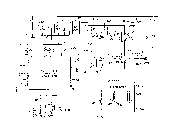
Reference is now made to the electrical schematic
diagram of Figure 1 which illustrates a charging system
100. An automotive alternator 102 is controlled to
provide a desired power o~u~ at a voltage level to
maintain the charge of an associated automotive battery
104. The voltage of the battery 104/alternator output
(BATT)~is monitored and its charging regulated by means
of an automotive voltage regulator 106 which can be an
integrated circuit commercially available, for example,
from Motorola Semiconductors and identified as an
MC3325. A first high voltage insulated gate transistor
108 preferably comprising a MOS insulated gate bipolar
transistor sold by IXYS and identified by the
designation IXGPlON90 is connected in series with and
between the battery 104 and a field w; n~i ng 110 of the
alternator 102. The transistor 108 is controlled to
selectively provide current from the battery 104 to the
field winding 110. A second high voltage insulated
gate transistor 112 preferably comprising a MOS
insulated gate bipolar transistor of the same type as
the transistor 108 is connected in parallel with the
field winding 110.
f,v
88-102 -8- 2 01~8 0 5
The transistor 108 is switched on and off under
the control of the voltage regulator 106 to pulse width
modulate the field current in response to the voltage of
the battery 104/alternator output (BATT) and the ambient
temperature. Battery voltage is monitored via a battery
sense conductor 114 connected between the battery 104 and
the voltage regulator 106. A gate voltage is continuously
applied to the transistor 112 under normal operating
conditions such that it circulates the current through the
field winding 110 when the transistor 108 is turned off.
However, while the transistor 108 is turned on, the
collector/emitter or drain/source of the transistor 112 is
reverse biased such that the transistor 112 is reverse
blocking and does not shunt the field winding 110 or
affect alternator regulation. In this way, when the
transistor 108 is switched off, the current through the
field winding 110 auto-commutates into the transistor 112
to maintain a desired regulated battery voltage or state
of charge of the battery 104.
The transistors 108, 112 are driven by a pair of
MOSFET drivers 116, 118, respectively, which are
commercially available, for e~ample, from Teledyne
semiconductor and identified by the designation TSC428.
The drivers 116, 118 are in turn driven by optocouplers
120, 122, respectively, commercially available from
Hewlett Packard and identified by the designation 6N137.
Power for driving the transistors 108, 112 is provided by
a 12V regulator 124 which can be a commercially available
LM340T12 and a DC/DC converter 126 which can be a
commercially available UR12-15D40. The converter 126
provides isolated + 15 volt outputs in response to a
regulated 12 volt input. A second 12V regulator 128
-\ 2015805
88-102 _9-
provides additional power for the optocouplers 120, 122
and a comparator circuit 130 which is used to turn off the
transistor 112 in a controlled manner in case of faults as
will become apparent. The optocouplers 120, 122 and DC/DC
converter 126 provide isolation between the voltage
regulator 106, the comparator 130 and the high voltages
generated on the transistors 108, 112 during normal and
fault operation.
If a fault occurs within a charging system
utilizing the alternator, such as the disconnection of the
battery 104 from the remainder of the system 100 or the
failure of an intercell connection within the battery 104,
a high voltage transient is generated at the alternator
- output (BATT) due to the sudden change in the alternator
output current when the battery current component goes to
zero. Such transients are due to the sudden current
change in the inductive stator 131, the self-inductance of
the field winding 110, the continuing field winding
current which couples the engine to the alternator and
residual iron magnetism. In the prior art, voltage
limiting and/or energy dissipating elements have been
connected to the alternator output (BATT), the field
winding 110 and/or the alternator 102 and associated
automotive equipment. For example, the voltage transient
generated on an automotive 12V bus by a current production
voltage regulator including conventional suppression
techniques is shown in Fig. 3 for a fault occurring at
8000 RPM and an 80 amp load on the alternator 102. While
this level of protection permits operation of an
automobile utilizing the charging system, it is
substantially greater than the transient generated under
the same operating and fault conditions by the method and
88-102 -10- 2 01 58 0 S
apparatus of the present invention as shown in Fig. 4.
With such reduced transients, overall system operation and
reliabilty are substantially improved.
If a fault occurs within the illustrated charging
system 100, the onset of an overvoltage transient is
sensed by the voltage regulator 106 and the comparator
130. In response to sensing the onset of what may well
have been a damaging overvoltage transient in the prior
art, the transistors 108 and 112 are turned off in a
controlled manner. In particular, the voltage regulator
106 nearly instantaneously (within approximately 1.5
microseconds) turns off the regulation transistor 108 and
the comparator 130 generates a turn off signal for the
transistor 112. The transistor 108 is turned off via the
transistor 132, the optocoupler 120 (note A-A
interconnection) and the driver 116. The transistor 112
is turned off via the comparator 130, the optocoupler 122
(note B-B interconnection) and the driver 118.
However, in the case of the transistor 112, a
resistor 134 is inserted into the base or gate circuit
such that the transistor 112 is "ramped" off or turned off
at a controlled rate. The resistor 134 in combination
with the gate capacitance of the transistor 112 forms an
RC circuit to ramp off the transistor 112 for fault
conditions. In the illustrated embodiment of Fig. 1, the
resistor 134 is selected to be 15K ohms which, in
combination with the capacitance of the gate of the
previously identifie~ MOSIGBT used for transistor 112,
provides a ramp time on the order of tenths of
milliseconds and has been determined to substantially
minimize the transient energy produced on the +12V bus 136
of the motor vehicle including the charging system 100.
88-102 -11- 2 01 ~8 0$
For example, the energy of the transient of Fig. 3 is
141.3 joules while the energy of the transient of Fig. 4
is reduced to 5.7 joules. Of course, different resistance
values can be selected for the resistor 134 dependent upon
the transistor 112 utilized and the desired ramp
characteristics of transistor turn off in the event of a
fault condition and the turn off of the transistor 112 can
be controlled in alternate ways, such as controlled steps
or the like, as will be apparent to those skilled in the
art.
An alternate embodiment of the invention
utilizing PNP transistors 108A, 112A is shown in Fig. 2 in
schematic block diagram form with like components being
assigned the same identifying numerals. A physical
structure of the PNP transistors 108A, 112A is illustrated
in this embodiment which may be desireable for formation
of the transistors 108A, 112A in the form of an integrated
circuit. As shown, the common collectors C or drains
tsubstrate) form the connection point for the field
winding 110 with top metalizations forming the two
emitters E or sources. Hybrid circuit, thick film
techniques are envisioned as being best to form a combined
regulator/gate drive circuitry with the two P-channel
devices existing as a single device.
The illustrated embodiments of the present
invention control the current in the field winding 110 of
the automotive alternator 102 of the battery charging
system 100 to maintain the battery voltage within defined
limits and to substantially suppress transients in the
event of faults in the charging system, such as
disconnection of the alternator 102 from the battery 104
or failure of intercell connections within the battery
~ 88-102 -12- 2 0 1 5 8 0 5
104. When such a fault occurs within the system 100, both
transistors 108, 112 or 108A, 112A are switched off in a
controlled manner to discharge the field winding energy at
an accelerated rate. The series connected transistor 108,
108A is nearly instantaneously turned off to remove the
source of field current and the parallel connected
transistor 112, 112A is then ramped off to act as a
controlled resistance and thereby dissipate the field
energy at a high voltage level within the parallel
connected transistor 112, 112A. By dissipating the field
energy at a high voltage level, the dissipation time is
substantially reduced as compared to prior art
arrangements.
It should be apparent that the present invention
is generally applicable to alternators used for
applications other than battery charging systems. For
example, a high voltage alternator may be used in the
automotive industry to power vehicle loads requiring high
power levels such as electrical air conditioning, four
wheel steering and the like. For such applications, the
alternator is disconnected from the load by power
switching operations. Such disconnections are effectively
the same as faults within a battery charging system in
that they generate high voltage transients at the output
of the alternator. Accordingly, the present invention is
equally applicable to such systems as well as dual voltage
level alternators and other alternator applications where
transients are generated either by load disconnections or
due to faults within the system. These alternate
applications may be accommodated by minor modifications of
the disclosed charging system as will be apparent to those
skilled in the art and therefore are not described in
detail herein.
2015805
88-102 -13-
Having thus described the alternator voltage
transient minimization method and apparatus of the present
invention in detail and by reference to preferred
embodiments thereof, it will be apparent that
modifications and variations are possible without
departing from the scope of the invention defined in the
appen~d claims.
.,~ .