Note: Descriptions are shown in the official language in which they were submitted.
iezoelectric Acceleration sensor and Piezoelectric
Acceleration Sensor Device
BACKGROUND OF THE INVENTION
Application Field of the Invention
This invention generally pertains to a piezoelectric
acceleration sensor and a piezoelectric acceleration sensor
device which use a film piezoelectric element. Specifically,
the piezoelectric acceleration sensor and sensor device
employ a simplified structure, which generates a small output
by an acceleration perpendicular to the sensing axis, and
offers excellent temperature characteristics and high impact
resistance.
Prior Art
A conventional piezoelectric acceleration sensor
(hereinafter referred to as "the sensor") in the public
domain is presented in Published Japanese Patent Application
56-10258. Th$s sensor has a disc-shaped diaphragm made of a
piezoelectric material (such as piezoelectric polymer) which
is fixed on a ring-shaped frame at its circumference. Both
sides of the center of the diaphragm have loading elements
which function as an inertial mass respectively. The frame
is fixed on a pedestal with the diaphragm suspended.
In the sensor, an axis crosses perpendicularly to the
film face of the diaphragm and runs through the center of the
loading element, which forms the acceleration sensing axis.
Such a sensor can detect an acceleration change ln the
sensing axis direction when a material to be measured is
~, -,-
~., ~ . :
- - .. ~ : ~ . - . . ..
.
,
At' ~
placed on the pedestal.
However, this sensor presents a problem: the loading
element produces a directional displacement even when an
acceleration is given in the direction perpendicular to the
sensing axis. This causes distortion in the diaphragm to
generate an electric output.
The sensor also has other drawbacks: its structure is
complex and its manufacture is difficult. Also, its
measurable frequency band is narrow and difficult to change.
A conventional piezoelectric acceleration sensor device
(hereinafter referred to as the sensor device) is known
publicly, which accommodates the sensor described in the
above Published Japanese Patent Application 56-10258. This
sensor device is bacically a circuit substrate mounted with
two components: an impedance conversion circuit which
converts an output from the sensor, and an amplification
circuit which amplifies the output. These are arranged side
by side in a enclosure. However, this sensor's inevitably
large size is undesirable.
SUMMARY OF THE INVENTION
In light of the above, the present invention is
intended to provide a piezoelectric acceleration sensor that
produces a relatively small output generated from an
acceleration in a direction other than the sensing axis.
This sensor must be easy to manufacture and be little
influenced by ambient temperature, and has good frequency
characteristics and impact reslstance. It must also be
.
,
:'
~ t2
compact.
This piezoelectric acceleration sensor (of the present
invention) contains the following: a pedestal installed
rigiclly on a body to be measured, a detecting element fixed
on the measuring plane perpendicular to a sensing axis of
this pedestal, and a loading element fixed on this detecting
element and made of a rigid material which acts as an
inertial mass.
This detecting element comprises a film piezoelectric
element, which is in a point symmetry with the sensing axis
as the center of the symmetry in a plane with the film plane
parallel to the said measuring plane. Metallic electrodes
are respectively bonded to both sides of the film
piezoelectric element, and at least one of these electrodes
is bonded to the film piezoelectric element by a dielectric
adhesive.
The loading element is in a point symmetry with the
sensing axis as the center of the symmetry in a plane
contacting the detecting element. When its cross section is
cut with innumerable planes passing through the sensing axis
and perpendicular to the said measuring plane, it is in a
line symmetry with the sensing axis as the symmetrical axis.
This structure reduces the output generated by an
acceleration in a direction other than the sensing axis. It
also elevates the lamination strength of each laminated
layer., and increases impact resistance.
This newly-invented sensor contains the following: a
pedestal rigidly installed on a material to be measured; a
sensing part fixed on a measuring plane perpendicular to the
., .
-, ' ~ :
'-
,, -
sensing axis of the ped~stal; and a loading element fixed onthe said sensing part, which is made up of a rigid material
acting as an inertial mass.
The said sensing part includes the film piezoelectric
element and two supporting plates made of a rigid material in
the form of a plate fixed on both sides of the film
piezoelectric element.
The heat conductivity of the material maintains the
supporting plates at less than 0.5 Wm 1 K 1. The plane of
the film piezoelectric element is in a point symmetry with
the sensing axis as the center of the symmetry in the film
plane parallel to the said measuring plane.
The loading element is in a point symmetry with the
sensing axis as the center of the symmetry in the plane
contacting the sensing part. When its cross section is cut
with innumerable planes passing through the sensing axis and
perpendicular to the said measuring plane, ~t is in a line
symmetry with the sensing axis as the symmetrical axis. This
structure oan reduce an output which has been generated
undesirably from a pyroelectric effect (caused by temperature
variations).
Another embodiment of the piezoelectric acceleratlon
sensor or measurlng acceleration of an ob;ect along a
predetermined axis of measurement comprises a base member, a
measurement unit, and a weight. The base member is attached
to the ob~ect. The measurement unit, extending in a plane
perpendicular to the predetermined axis of measurement, is
supported by the base member, and comprises a piezoelectrio
membrane, and a pair of electric terminal plates attached to
both s~rfaces of the piezoelectric membrane. At least one of
said electric ter~inal plates is composed of a plurality of
sections separated from one another. The weight is attached
to at least one of said sections, the weight means having
cross-sections, in any plane perpendicular to the
predetermined axis, symmetric with respect to a point whereat
the axis crosses the cross-section, wherein the terminal
plates to which the weight means are attached are
electrically connected with the terminal plates to which the
weight means are not attached. The sensor of this structure
also reduces the output variations caused by a pyroelectric
effect.
Moreover, the sensor device contains the following: the
pedestal: the sensing part formed by the film piezoelectric
element being held between the supporting plates; and a
processing circuit which processes the electrical output from
the film piezoelectric element into the sensor (this consists
of the loading element fixed on this sensing part, and is
made up of a rigid material which acts as an inertial mass
and is installed on the opposite side of the measuring plane
of the said pedestal). The said assembly is accommodated and
fixed in a hollow enclosure with the sensor supported in the
hollow enclosure only around the pedestal. The pedestal and
the enclosure may be of various shapes so long as support is
supplied at the periphery. The pedestal and the enclosure
are, for example, not limited to a cylindrical nor a c~rcular
shape, but may be of other shapes as well.
The film piezoelectric element is in a point symmetry
~3
with the sensing axis as the center of the symmetry in a
plane with the film plane parallel to the said measuring
plane. The loading element is in a point symmetry with the
sensing axis as the center of the symmetry in a plane which
contacts the film plezoelectric element. When its cross
section is cut with innumerable planes passing through the
sensing axis and is perpendicular to the said measuring
plane, it is in a line symmetry with the sensing axis as the
symmetrical axis. The structure of this sensor makes the
whole device more compact, and renders the sensor itself less
influenced by temperature variations in the external
environment.
BRIEF DESCRIPTION OF THE DRAWI~GS
Fig. 1 i~ a perspective view of an example of the
sensor in the first embodiment of the present invention.
Figs. 2 through 7 are plan views of examples of the
plane shape of the film piezoelectric element.
Figs. 8 through 14 are cross sectional views of
examples of the three-dimensional shape of the loading
element.
Fig. 15 is an exploded perspective view of an example
of the sensor in the second embodiment of the present
invention.
Fig. 16 is an exploded perspective view of an example
of the sensing part of the sensor in Fig. 15.
Fig. 17 is an exploded perspective view of another
example of the sensing part.
,. .~. .
2 0 ~
Figs. 18 through 20 are plan views of an example of the
plane shape of supporting plates used in the sensor in the
seconcl embodiment.
Figs. 21 and 22 show the third embodiment of the
present invention. Fig. 21 is a side view and Fig. 22 is a
perspective view.
Figs. 23 and 30 are wiring diagrams of the divided
electrodes of the sensor shown in Eig. 21.
Figs. 24 through 29 are views of the electrodes on the
front and rear surfaces of the film piezoelectric element in
the third embodiment.
Figs. 31 and 32 are cross sectional views of examples
of the sensor device of the present invention.
DETAILED DESCRIPTION OF THE PREFERRED EMBODIMENTS
The following is a detailed description of the
preferred embodiments of the present invention, with
reference to the drawings.
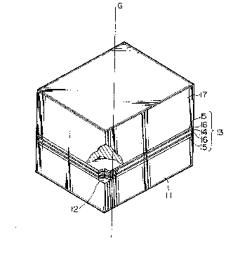
Fig. 1 shows the flrst example of the sensor; the
numeral 11 in the figure indicates a pedestal. The pedestal
11 forms the basic body of the sensor, is installed rigidly
on the material to be measured, and is made of a suitably
rigid material, such as steel, brass or aluminum. The
coefficient of elasticity of the material which forms
pedestal 11 exceeds that of the film piezoelectric element as
explained later, and the thickness of pedestal 11 should
preferably be several times that of the film piezoelectric
element.
Pedestal 11 shown in the figure is of a rectangular
2 0 ~
parallelepiped shape, but is not limited to this shape: it
may, for example, be disc- or column-shaped, and may be of
other shapes as well.
Pedestal ll has one flat and smooth surface as a
measuring plane 12. Measuring plane 12 ~ust be precisely
perpendicular to the sensing axis G of the acceleration
sensor.
On measuring plane 12 of pedestal 11, a detecting
element 13 is fixed integrally and securely to the pedestal
ll. To fix pedestal ll and detecting element 13, a
hardenin~-type adhesive such as an epoxy adhesive is used;
this adhesive ~not shown in the figure) formæ a bonded layer
between pedestal 11 and detecting element 13.
Detecting element 13 contains a film piezoelectric
element 14 and metallic foil electrodes 15, the latter being
arranged on both sides of element 14, the metallic electrodes
15 and 15 being bonded to the film piezoelectric element 14
respectively by dielectric bonded layPrs 16 and 16 made of a
dielectric adhesive.
The film piezoelectric element 14 uses a plezoelectric
material with a thickness of 10 to 500 microns, the thic~ness
being su$ficiently uniform and the quality being sufficiently
homogenous. The piezoelectric m~terial typically
includes the following: polyvinylidenefluoride (PVDF~,
polyvinylidenechloride, polyvinylfluoride, polyvinylchloride,
nylon including nylon ll and polymetaphenyleneisophthalamide,
copolymers of tetrafluoroethylene, trifluoroethylene, vinyl
fluoride with vinylidene fluoride, copolymers of vinyl
- . ,
'
~ 3 ~ l~
acetate and vinyl propiona-te. It also inc]udes vinyl
benzoate with vinylidene cyanide, polymers such as blended
polymers of polyvinylidenefluoride with polycarbonate,
blended polymers of polyvinylidenefluoride with
polyvinylfluoride, as well as piezoelectric powders such as
metatitanate and titanate zirconate added and dispersed in a
polymer.
Film piezoelectric element 14 may use many films
laminated by dielectric adhesive, rather than using a single
film, and the thicker the total thickness, the more the
output, which is desirable. The f$1m piezoelectric element
is made of a fluororesin such as polyvinylidenefluoride and
should preferably have its surface activated by a surface
treatment using sodium. The treatment increases its adhesion
to the metallic electrode 15 and improves impact reslstance.
Metallic electrode 15 uses various kinds of metallic
sheets, including aluminum and copper foils with a thickness
of 10 to 500 microns.
The dielectric adheslve to form the dielectric bonded
layer 16 should preferably have a dielectric constant of more
than ~.5. It is best to use such adhesives as epoxy, phenol
and the cyanoacrylate series.
In the detecting element 13 of the above structure, the
metallic electrodes 15, the latter are arranged on both sides
of film piezoelectric element 14 with the dielectric bonded
layers 16, the latter interposed. Because the dielectric
bonded layer 16 is formed by the dielectric adhesive, the
detecting element 13 functlons as a capacitor, thereby making
it possible to remove the output of the film piezoelectric
~3~2
element 14 from across the metallic electrodes 15 and 15.
The planar shape of detecting element 13 and film
piezoelectric element 14 is significant in reducing
transverse sensitivity.
The transverse sensitivity in the present invention
refers to an output Pl when applied with an acceleration in
the direction of the sensing axis G of the sensor, and an
output P2 when applied with an acceleration in a direction
perpendicularly crossing the sensing axis G. This is
expressed as the ratio of P2/P1.
The planar shape of the piezoelectric film 14 must be
in a point symmetry with the sensing axis G as the center of
the symmetry in a plane parallel to the measuring plane 12.
The shape shown in Fig. 1 is that of a rectangular
parallelepiped. Other shapes that meet this requirement are
shown in Figs. 2 through 7. Fig. 2 shows a parallelogram,
Fig. 3 a circle, Fig. 4 an ellipse, Fig. 5 a regular hexagon,
Fig. 6 a regular octagon and Fig. 7 a ring. The symbol G in
these figures indicate the sensing axis G. All of these
planar shapes are in a point symmetry with the sensing axis G
as the symmetrical center. Needless to say, other shapes
that satlsfy the above requirement can be used.
On the detecting element 13, is integrally fixed a
loading element 17 made of a rigid material and acting as an
inertial mass. Loading element 17 is displaced when applied
with an acceleration, and generates a distortion or a strsss
in the film piezoelectric element 14. Its weight is not
especially limited, because it relates to an electrical
.
. ~ .
. ~
OUtp~lt per unit acceleration of the sensor. It sh ~ ~i
however, be in a range that will not generate a creep in the
film piezoelectric element 14. Loading element 17 is fixed
to detecting element 13 in a manner similar to pedestal 11
being fixed to detecting element 13.
The three dimensional shape of loading element 17 plays
an important role in reducing the transverse sensitivity.
First, the face of loading element 17 which contacts
detecting element 13 (hereinafter called the bottom face)
needs to be precisely perpendicular to the sensing axis G,
and the planar shape of the bottom face must be in a point
symmetry with the sensing axis G as the symmetrical center.
Therefore, since the planar shape meets this requirement,
those shown in Figs. 2 through 7 can be used, as in the case
of detecting element 13 and film piezoelectric element 14.
However, in a combination of detecting element 13 and loading
element 17, the planar shape of the bottom face of loading
element 17 does not have to be the same as that of detecting
element 13. For example, the planar shape of detecting
element 13 of a regular square may be combined with that of
the loading element of a circle, as long as the combination
has the same sensing axis G.
At the same time, when the loading element 17 is
crosscut into innumerable planes passing through the sensing
axis G and perpendicular to the bottom face, it must be in a
line,symmetry with the sensing axis G as the symmetrical
center, relative to all the cross sections. Those satisfying
the line symmetry requirement are shown in Figs. 8 through
14. Fig. 8 shows a plate, Fig. 9 a column, Fig. 10 a cone,
11
:
'
Fig. 11 a sphere cut by a plane, Fig. 12 an ellipse cut by a
plane, Fig. 3 a column formed with a hollow section inside,
and Fig. 14 a ~ombination of the column and plate. In these
figures, the symbol S indicates the bottom face and the
symbol G indicates the symmetrical axis coinciding with the
sensing axis. Therefore, loading element 17, to satisfy the
line symmetry requirement, must have its center of its
gravity on the sensing axis G. In addltion, the loading
element 17, besides being made of the same ~aterial, can be
made of a composite material consisting of different
materials. However, in this case, each material must be able
to bind securely with the others to form a material that can
be regarded as a wholly rigid material, with each material
not causing different displacements when applied with an
acceleration.
Furthermore, a loading element with many divided
loading elements (having different masses) laminated along
the sensing axis G can be used as the loading element 17.
The laminates of the divided loadiny element enable fine
ad~ustment of the sensor output. In the loading element
using the laminates, it is preferable to make it satisfy the
relation of the following equation to eliminate a noise
influence caused by the pyroelectric effect:
0-8 (KB/tB) ~ (Kw/tw) ~ 1-2 (KB/tB), where tB is the
thickneæs of pedestal 11, KW is the heat conductivity of the
divided loading element directly above detecting element 13,
and tw is the thickness of the divided loading element.
Moreover, to produce loading element 17 out of a
12
:
2~ 2
magnetic mate~ial such as iron or an iron alloy, and to
dispose a magnetic field genera~ing coil in the vicinity of
the sensing axis G of loading element 17, will make it
possible to self-diagnose the output calibration and the
degradation of the sensor. That is to say, when the magne$ic
field generating coil is energized, a magnetic attracting or
repulsive force acts on loadlng element 17, and causes an
output from film piezoelectric element 14. Since this output
is maintained at a certain value because of the magnetic
field generating coil, output calibration and degradation can
be determined.
For loading element 17 to satisfy this requirement,
(that is, to have the symmetrical characteristic), it must be
arranged and fixed with its symmetrical axis coinciding with
the symmetrical center of detecting element 13. In other
words, the symmetrical center of detecting element 13 should
coincide with the symmetrical axis of loading element 17.
The sensor of this structurs is used with pedestal 11
fixed on the material to be measured, to measure an
accel~ration in a directton of the sensing axis G.
The sensor of this structure produces very little
transverse sensltivity, because the planar shape o~ detecting
element 13 and it~ film piezoelectric element lg is in a
point symmetry with tha sensing axis G as the symmetrical
center, and the planar shape of the bottom face of loading
elembnt 17 is in a point symmetry with the sensing axis G as
the symmetrical center. At the same time, the three
dimensional shape of loading element 17 is in a line symmetry
with the sensing axis G as the symmetrical axis in all the
1~
2 ~ ~ ~ 8 ~ 2
planes passing through the sensing axis G.
Generally, when an acceleration is applied to the
sensor in a direction other than its sensing axis direction,
the acceleration is divided according to the vector
resolution law into a component of at least two directions
perpendicularly crossing the sensing axis and a component of
the sensing axis direction. The component which
perpendicularly crosses the sensing axis acts on the center
of gravity of loading element 17 to cause a bending momPnt
around the gravitational center acting on loading element 17.
Therefore, a compressive force acts on part of film
piezoelectric element 14 in detecting element 13, and a
tensile force on the remaining part. Film piezoelectric
element 14 generates electrical charges of opposite signs
because of the compresslve and tensile forces. If~ however,
the charges are equivalent in amount, these cancel each other
out, which results in no output. Therefore, if compressive
and tensile forces of the same amounts are applied to the
film piezoelectric element, the latter will not output any
output, and the sensor will not detect the acceleration in a
direction other than the sensing axis.
In the present invention, because the respective shapes
of detecting element 13 (film piezoelectric element 14) and
the loading element 13 are given the symmetrical
characteristic as descr~bed above, film piezoelectric element
14 is applied with the same amounts of compressive and
tensile forces, even if ~he acceleration in a direction other
than the sensing axis is given, thereby making film
~4
2 ~ 2
piezoelectric element 14 produce no output, making the
transverse sensitivity very small.
In addition, the sensor can have a high upper limit of
the measurable frequency, and a wide measurable frequency
band. The upper limit of the measurable frequency of this
type of the sensor is determined by the resonant frequency of
the sensor. Because the resonant frequency of the sensor of
the present invention is, structurally, in proportion to the
values of elements which exist between pedestal 11 and
loading element 17, (that is, the coefficients of elasticity
the adhesive layer, the dielectrically bonded layer 16 and
film piezoelectric element 14, divided by the mass of loading
element 17), the resonant frequency is over two orders of
magnitude than that of the conventional diaphragm type
sensor, and i8 on order of kilohertz. However, care should
be taken that the resonant frequency decreases as the
coefficient of elasticity of the adhesive layer decreases.
In this case, the effect of the metallic electrode 15 can be
ignored, since it is regarded as a rigid material.
For this reason, the structure which uses an adhesive
to fix detecting element 13 with pedestal 11 and loading
element 17 must satisfy the relationship presented by the
following equation:
(EA/tA) / (Ep/tp) 2 0.1, where EA is the coefficient of
elasticity of the adhesive layer and the dielectrically
bonded layer 16, tA is the total thickness of the adhesive
layer and the dielectric bonded layer, Ep is the coefficient
of elasticity of the film pie~oelectric element 14, and tp is
its thickness.
The coefficient of elasticity of the adhesive layer and
the dielectrically bonded layer in the above equation is
determined by calculating the ratios of the coefficient of
elasticitys of the respective bonded layers to the thickness,
summed, and substituted into the above equation.
What this equation refers to is a condition that the
force generated in loading element 17, as a result of the
acceleration, is transmitted to film piezoelectric element 14
without being absorbed and decreased by the adhesive layer
and the dielectrically bonded layer. If the value of the
above equation equals less than 0.1, the absorption and
decrease of the force by the adhe~ive layer and the
dielectric bonded layer can no longer be ignored, or this
will result in a decrease of the resonant frequency, and a
narrowing of the measurable frequency band as described
above.
Therefore, the adhesive used to attach detecting
element 13 to pedestal 11 and the detecting element to
loading element 17, and the dielectric adhesive, must be
selected from a hardening adhesive of high coefficient of
elasticity, such as epoxy, phenol or the cyanoacrylate
series. Adhesion using rubber series adhesive is inadequate.
Because the sensor of this structure has pedestal 11,
detecting element 13 and loading element 17 simply laminated,
the structure is simplified. It also facilitates
manufacture, and makes the device more compact. Also,
because the metallic electrodes 15 and 15 are bonded securely
to film piezoelectric element 14 by dielectrically bonded
.
,
2 ~
layers 16 and 16, the sensor has sufficient st~ength against
an impact against not only its direction of thickness b~t
also its face direction (a direction perpendicularly crossing
the sensing axis G). In addition, disposing such metallic
electrodes 15, the latter serves to simplify the wiring to
remove electrical signals. It also makes various bonded
technologies used in semiconductor manufacturing applicable,
and makes connection with various printed cards, for example
flexible printed circuit (FPC), possible.
In the example described above, the detecting element
13 is formed by film piezoelectric element 14 and metallic
electrodes 15 and 15 disposed on lts both sides, and metallic
electrodes 15 and 15 are constructed by attaching them to
film piezoelectric element 14 using the dielectric bonded
layers 16 and 16. However, the structure need not be limited
to this construction; metallic electrode 15 can be attached
to one face of film piezoelectric element 14 through
dlelectric bonded layer 16, and another metallic electrode
can be disposed directly on the other face using a deposition
process.
[Embodiment 1]
An aluminum sheet wlth a thickness of 1.0 mm was
prepared to form the material of the pedestal. Copper foils
having a thickness of 30 microns were bonded onto both sides
of th~ vinylidene fluoride sheet having a thickness of 110
microns(a film piezoelectric element) us~ng an epoxy adhe~ive
(product name: "Araldite" made by Ciba-Geigy), and the sheet
was cut to a size so that the bottom face will be a sguare of
;
10 mrn on a side to be used as a chip. The bonded layers
(dielectric bonded layers) have a thickness of about 15
microns in this case, and the coefficient of elasticity of
the film piezoelectric element is 2.7 x 10⁹ Pa.
Next, the bottom face of the chip was bonded to the
said aluminum sheet using an epoxy adhesive, and the loading
element was bonded on top of the chip using the epoxy
adhesive. In bonding the loading element, the film
piezoelectric element of the said chip and ths loading
element were arranged so that their symmetrical axes
corresponded with each other. The thickness of each of the
bonded layers is about 20 microns. The loading element, made
of brass, has a square bottom face with si~es of 10 mm, a
height of 5 mm, and a mass of 4.2 g. The coefficient of
elasticity of the adhesive used is 3.5 x 10⁹ Pa.
[Embodiment 2]
Aluminum was directly vacuum deposited on one face of
the polyvinilydenefluoride sheet 1 to form an aluminum
electrode, and a copper foil 30 microns thick was bonded to
the other face using an epoxy adhesive in a simllar manner to
Embodiment 1, and cut to a square chip with sides of 10 mm.
Next, the bottom face of the chip was bonded to the
aluminum sheet that forms the pedestal, using an epoxy
adhesive in a manner similar to Embodiment 1, and the same
loading element (as the one in Embodiment 1) was bonded on
top of the chip in a similar manner.
18
: : . .. . .
-
.
,
2 ~ 2
[Emb~diment 3]
A sensor was fabricated in a manner similar to
Embodiment 1, except that a column with a diameter of 14 mm
and a weight of 4.2 g was used as a loading element.
tEmbodiment 4]
A sensor was ~abricated in a manner si~ilar to
Embodiment 3, except that a disc-shaped chip with a diameter
of 14 mm was used.
(Comparison 1)
A sensor described in Embodiment 1 was fabricated with
the symmetrical axis of the loading element and the chip
intentionally shifted by 1.5 mm.
(Comparison 2)
A sensor described in Embodiment 2 was fabricated usin~
a chloroprene adhesive to bond the loading element with the
chip. The thickness of the bonded layer was about 30 microns,
and the coefficient of elasticity was 7 x 10⁶ Pa.
(Comparison 3)
An aluminum sheet of the same specification as the one
used in Embodiment 1 was prepared for a pedestal. Aluminum
was directly deposited on both faces of the fluorovinilydene
sheet (the piezoelectric element) (which had a thic~ness of
110 mlcrons) to form a deposited aluminum electrode, and cut
to a square chip with sides of 10 mm.
Next, the bottom face of the chip was bonded to the
aluminum sheet that forms the pedestal, using an epoxy
adhesive in a manner similar to Embodiment l, and the same
19
'
.
.
loading element ( as the one in Embodiment 1) was bonded on
top of the chip in a similar manner.
(Comlparison 4)
As aluminum sheet of the same specification as the one
used in Embodiment 1 was prepared for a pedestal. A 110
micron-thick fluorovinllydene sheet (piezoelectric element)
was cut to a square with sides of 10 mm a dielectric paste
was coated on both sides of the sheet; and the pedestal and
the loading element were bonded over the paste to form a
sensor assembly.
The thickness of each dielectric paste layer is 20
microns, and the coefficient of elasticity is 2.0 x 10⁹ Pa.
(Conventional structure 1)
The film piezoelectric element used in Embodiment 1 was
cut to a 20 mm diameter disc to form a vibration sheet.
Hemispheres of polymethylmethacrylate were fixed on both
sides of the vibration sheet at its central axis to form an
inertial mass, and the circumference of the vibration sheet
was bonded to a ring-shaped frame using an epoxy adhesive to
form a sensor. The sensor is identical with the one laid
open in Japanese Patent Application No. 56-10258.
(Conventional structure 2)
A film piezoelectric element made of
polyfluorovinylidene which has a thickness of 30 mlcrons was
bondsd to a vibration sheet made of copper which has a
thlckness of 30 microns, uslng an epoxy adhesive.
This element was fixed in a ring shaped frame to form a
ZO
. ' ' , '. .'' : . . ' ' ' . ; ' . :' . ~. ~'- :
,,, . : , .
'.. ' ': :, ~
. .
2Q1 3 S ~ 2
vibration part with a diameter of 15 mm, and a 7 mm diameter
hole was drilled in its center to form a sensor.
(Conventional structure 3)
A film piezoelectric element made of
polyfluorovinylidene which has a thickness of 50 microns was
bonded to a brass plate which has a thickness of 0. 5 mm,
using an epoxy adhesive. This element was cut to an oblong
shape of 5 mm wide and 35 mm long, and a hole of 2 mm
diameter was drilled through its center. The oblong plate
was bent to a bow shape with the radius of curva~ure at 70 mm
80 that the film piezoelectric element is on its outside~
This element was used as a three-point supporting type
vibration beam with a screw inserted into the through hole to
provide a concavity, and was attached to the pedestal to
perform as a sensor.
The following performance evaluation tests were
conducted on these sensors of the embodiments, comparisons
and conventional structure.
The output of each sensor is outputted as a voltage
using an impedance conversion circuit connected to the
sensor.
The following items were evaluated in the performance
evaluation test according to acceleration detection.
(1) Sensor output V per lG in the sensing axis (a value after
correcting the gain obtained in the impedance conversion
circuit) and the minimum detecting acceleration (s/n - 3),
where G is the gravitational constant (9.8 m/s2).
(2) Measurable frequency range ~a range of ~10% of the output
21
2 ~ ' 2
at central frequency).
(3) Crosstalk (the ratio of an output when lG acceleration is
given to a direction perpendicular to the sensing axis to a
lG output in the sensing axis, indicated in percent).
In addition, impact resistance was evaluated.
The impact resistance test consisted of destroying the
sensor chip by applying an impact acceleration of 5000G from
a direction lateral to the sensor, and the number of impact
accelerations given before the sensor chip was destroyed were
counted. The results are shown in Table 1.
Table 1
_ .
Conventional
structure Embodiment Comparison
Sensor 1 2 3 1 2 3 4 ~ 2 3 4
output12.7 1.4 5.7 3.5 3.6 3.52.7 3.4 3.63.5 3.5
(rms)
mV/G
. _
Minimum
dietgct 0.02 0.1 D.05 0.05 0.05 0.05 0.05 0.05 0.05 0.04 0.05
accel-
tion
~ _ _ .
Measur
-able 0.1- 1- 1- 1- 1- 1- 1- 1- 1- 1- 1-
quency 150 300250 5K 5K 5K 5K 4.5X 5005K 4.5K
band(Hz~ _ _
CrOBB - 3514 23 3 ~ 5 3 25 4 4 5
Impact .
resist 172 168 138156 65 160 190 145 66 2 3
-ance
(cycle) ~ ~ _
~2
,
.,,
-
-
2 ~ 2
Fig. 15 is the second embodiment.
In this sensor, a sensing part 18 is bonded lntegrallyto pedestal 11 on its measuring plane 12 using an epoxy
adhesive.
Sensing part 18 consists of disc-shaped supporting
plates 19 and 19 bonded on both sides of a disc-shaped film
piezoelectric element 14. Film piezoelectric element 14,
described in the previous example, is used in thi~ case, and
both its sides are bonded with metallic electrodes to remove
an output ~not shown) over a dielectric adhesive (not shown).
Film piezoelectric element 14 does not have to be a single
sheet a structure laminating more than two sheets using a
dlelectric adhesive may be adopted.
For the supporting plate 19, a sheet material with
sufficient rigidity and heat conductivity of less than 0.5
Wm 1 K 1 is used. This includes, for example, ceramic
sheets, glass sheets, and sheets of fiberglass-reinforced
plastic (FRP) such as fiberglass-reinforced epoxy resin and
fiberglass-reinforced polyester resin, each having a
thickness of 0.5 mm to 2 mm. If the heat conductivity
exceeds 0.5 Wm 1 K 1, film piezoelectric element 14 transmit~
the external temperature variations to increase output
variation caused from the pyroelectric effect. ~onding film
piezoelectric element 14 with supporting plate 19 uses an
epoxy adhesive. The sensing part thus made becomes a rigid
plate as a whole, building the thickness to several
millimeters to facilitate handling.
The planar shape of the film piezoelectric element equal
23
,
~`~
symmetry is described in the previous embodiments.
In addition, sensing part 18 has loading element 17
attached to it by an epoxy adhesive. This loading element 17
i8 identical with the ones shown in the previous embodiments,
and so is the symmetry required in the planar shape.
In this sensor, the adhesive used for bonding sensing
part 18 itself, and with pedestal 11 and loading element 17
needs to satisfy the relationship expressed by the following
equation:
(EA/tA) / (Ep/tp) 2 0.1, where EA is the composite equivalent
coefficient of elasticity of the adhesive layer and
supporting plate 19, tA is the sum of the thickness of these
elements, Ep is the coefficient of elasticity of the film
piezoelectric element 14, and tp is the thickness.
If the klnd of adhesive and the coefficient of
elastlcity differ, the ratio of the coefficient of elastlcity
and thickness at each adhesive layer is obtained, and
substituted in the equation.
In this sensor, sensing part 18 is a rigid element with
a thickness of several millimeters, thereby making handling
easy and reducing the labor in manufacturing. In addition,
since the heat conductivity of supporting plate 19 is less
than 0.5 Wm~l K-l, the variation of the atmospheric
temperature outside the sensor is sufficiently moderated
time-wise, and transmitted to film piezoeleatric element 14.
Therefore, the output ~rom film piezoelectric element 14
generated from the pyroelectric effect becomes very small,
which improves the temperature characteristics of the sensor
24
~utput.
Fig. 17 iS another example of sensing part 18. The
latter is made up of a disc-shaped film piezoelectric element
14 having on its both sides the supporting plates 19 and 19
formed with a notch 20. Supporting plate 19 used in this
structure is also made of a material which has the heat
conductivity of less than 0.5 Wm~1 K~1 with the same disc-
shape as film piezoelectric element 14, but has the
semicircular notch 20 formed on part of it. Notch 20 should
have an area of less than 25~ of the area of film
piezoelectric element 14. An area exceediny 25% impairs the
symmetrical characteristic of element 14 so that it detects
an acceleration in a lateral direction, resulting in larger
transverse sensitivity, reduced bonding area and bonding
strength, as well as decreased impact resistance. Notch 20
should be open to the outslde of support~ng plate 19. The
shape of notch 20 has no limltations, and a square-shaped
notch may be used in place of the semicircular notch shown in
Fig. 17. The two supporting plates (19 and 19), however,
must have notches of an identical shape. In bonding the two
supporting plates on both sides of film piezoelectric element
14, supporting plate 19 ~ormed with notch 20 must be arranged
~o that when one of supporting plates 19 is rotated 180
degrees with respect to the sensing axis G as ths rotation
center, notch 20 will lie completely upon notch 20 of the
other ~upporting plate l9 with an exact correspondence in
position. If this condition i~ not met, sensing part 18 will
be unsymmetrical, worsening the sensor cross talk.
Figs. 18 through 20 show the variations of supporting
2 ~ 2
plate 19 of the above example. Supporting plate 15 (shown in
Fig. 18) is combined with film piezoelectric element 14 of a
disc-shape (shown in Fig. 1), and supporting plate 15 (shown
in Flg. 20) is combined with film piezoelectric element 14
(shown in Fig. 3). Notch 20, indicated by broken lines in
Figs. 18 through 20, is the notch on the other supporting
plate 19 when two supporting plates 19 and 19 are arranged on
both sides of film piezoelectric element 14. It is visible
that notch 20 lies upon the other notch when the other
supporting plate 19 is rotated 180 degrees with the sensing
axis G as the rotating axis.
Such a sensing part 1~ as described above has a
thickness of several millimeters, and forms a rigid element
which makes handling easy, and allows a lead wire or terminal
to be installed on the film piezoelectric element, utilizing
notch 20 on supporting plate 19. In addition, because
notches 20 are arranged symmetrically on supporting plates
19, the symmetrical characteristic of sensing part 18 as a
whole i8 not appreciably impaired, and the transverse
sensitivity is not aggravated.
[Embodiment 5]
A 5 mm thick aluminum plate was used as a pedestal on
which a sensing part was bonded uslng an epoxy adhesive. The
sensing part uses a glass epoxy plate (supporting plate) of a
regular square with the sides of l cm in length each, having
a thickness of 1 mm and heat conductivity of 0.2 Wm~1 K 1
bonded on both sides of a polyfluorovinylidene film (disposed
with an aluminum deposited electrode) of a regular square
26
~1 5~ S~
with sides of 1 cm in length each, having a thickness of 100
microns as a film piezoelectric element. On this sensing
part is bonded a loading element made of brass having a
bottom face of a regular square of 1 cm x 1 cm and a weight
of 10 g, to form a sensor.
The coefficient of elasticity of the
polyfluorovinylidene fllm is 2.7 x 10⁹ Pa, the composite
equivalent coefficient of elasticity of the adhesive layers
and the glass epoxy plate (supporting plate) is 1.6 x lO9 Pa,
and the thickness of the adhesive layers is about 14 microns.
(Comparison 5)
A sensor was fabricated in a manner similar to
Embodiment 5, except that an aluminum plate (of a 1 cm by 1
cm square with thlckness of 1 mm) was used as the supportlng
plate of the sensing part.
(Comparison 6)
A sensor was fabricated in a manner similar to
Embodiment 5, except that an epoxy resin filled with copper
powder formed in a plate (wlth thickness of 1 mm and heat
conductivity of 1 Wm 1 K 1) was used as the supporting plate
of the sensing part.
These three kinds of sensors were tested for their
temperature characteristlcs. The test conslsted of blowlng
heated air on the sensors to rapidly vary the temperatures in
the vicinity of the sensors. Evaluation was then made
regardlng the output variation per unit temperature (1C).
`:
.
',
2~ ~ ~3~2
The output is expressed as a ratio to 1 G output of the
sensor. The results are shown in Table 2.
Table 2
_ Output variation because of
temperature variation (G/C)
.
Embodiment 5 0.1
Comparison 5 1.3
Comparison 6 0.7
Flgs. 21 and 22 show the third embodiment. In this
sensor, film piezoelectria element 14 is fixed on the
measuring plane 12 of pedestal 11 through a bonded layer. On
the upper surface of thls film piezoelectric element 14, are
attached square-shaped electrodes A and B, made of aluminum
foil, to take out alectrical outputs. These have an area of
about half that of film piezoelectric element 14. On the
rear surface of film plezoelectric element 14 is fixed an
electrode C that covers the entirety of the rear surface.
The said electrodes A and ~ are attached with a clearance
between them of several millimeters (preferably less than 3
mm, and as small as possible) on the upper surface of fllm
piezoeleotrlc element 14.
In addition, on electrode A on the surface side of film
piezoelectric element 14, loadlng element 17 (made of a rigid
matqrial and unctioning as an inertial mass) is integrally
bonded, covering the upper surface of electrode A through the
adhesive layer.
Figs. 23 and 24 show an example of wiring structure to
28
.
: ' , , -:
-
, '' ~
obtain electrical ou-tputs from each electrode in the sensor
of the above-mentloned construction. In the wiring structure
of this example, when electrode A on the film piezoelectric
element 14 and electrode B on the film piezoelectric element
14 are respectively applied with an identical temperature
variatlon and an identical distortion, electrode A and B
generate an identical voltage and electric charge
respectively. Therefore, the wiring is so arranged that
these voltages and electric charges are canceled out.
In other words, as the polarizing direction of the film
piezoelectric element 14 is disposed upward in this example,
as shown in Fig. 23, a lead wire 21 can be connected to
electrode A of the film piezoelectric element 14 and a lead
wire 22 to the electrode B ln order to take out the voltage
or the electric charge.
The shape of the electrodes formed on both sides of film
piezoelectric element 14 is not limited to the above-
mentioned example. For example, as shown in Fig. 25, the
film piezoelectric element may be formed in a regular square,
while electrodes A and B may be formed in oblongs of
different sizes. Furthermore, if the film piezoelectric
element 14 i~ formed in a regular sguare, as shown in Fig.
26, electrode B may be formed in a ring along the
circumference of film piezoelectric element 14, and electrode
A may be formed inside the ring. If the film piezoelectric
element 14 is formed in a circle, as shown ln Fig. 27,
electrode B may be formed in a ring along the circumference
of fllm piezoelectrlc element 14, and electrode A may be
?~
:
1 2
formed inside the ring.
It is also possible to divide into a plurality the
electrode on the rear surface of film piezoelectric element
14, as shown in Figs. 28 and 29.
In the example shown in Fig. 28, the upper surface of
the oblong film piezoelectric element 14 is divided into two
electrodes A and B, while the electrode on the rear surface
is divided into two square electrodes A' and B'.
In the example shown in Fig. 29, the upper surface of
the circular film piezoelectric element 14 is divided
identically, as in the example shown in Fig. 27, while the
electrode on the rear surface is divided into electrode A' of
an approximately circular form and electrode ~' of a ring
form.
In the structure shown ln Flgs. 25 through 29, the
loading element 17 is bonded on either electrode A or
electrode B.
As described above, the shapes of the film piezoelectric
element and the electrodes, as well as their wiring
structures, can be formed in many ways, as shown in Figs. 24
through 29. However, there are certain restricting
relationships between the wiring struature and the area of
the electrodes.
That is, when removlng the output as a voltage, there is
~o special restriction on the electrode araa if the wirlng
has a serial connection structure, as shown in Figs. 24
through 27, but in the case of a parallel connectlon
structure, as shown in Figs. 28 and 29, it is preferable to
make the areas of electrode A and electrode ~, and of the
:::
20 ~ ~8~2
electrode A' and electrode B', all equal.
When removing the output as an electric charge, it is
preferable to make each area o~ electrode A and B equal for a
serial connection as shown in Figs. 24 through 27, and, in
the parallel connection, the areas of electrodes A, B, A' and
B' are all equal, as in Figs. 28 and 29.
The above explanation referred to an example of the
electrode of film piezoelectric element 14 divided ln two,
but it goes without saying that the electrodes of film
piezoelectric element 14 can be divided into three or more.
In this case, the loading element 17 may be bonded on each of
the divided electrodes, or on just one of the divided
electrodes.
Wlth respect to the symmetry of the plane shape of film
piezoelectric element 14 and the symmetry of the three
dimen~ional shape of the loading element 17, the condition
described in the first embodiment will apply.
According to the embodiment described above, the
separated electric terminals were attached to the upper side
of the piezoelectric membrane. However, the terminals can
also be attached to the lower æide of the piezoelectric
membrane. In the latter case, a weight having a cross
section substantially identical to that of the electric
terminal is attached to the upper side of the piezoelectric
memebrane so that the membrane is sandwiched by the weight
and one of the electric terminals. The electric terminals
can be attached to the piezoelectric membrane by virture of a
dielectric adhesive. Supporting plàtes may be attached to
31
the electric terminals. In this case, the weight is attached
to one of the electric terminals. In any variations
mentioned above, electric terminals are connected to each
other before or after the impedence conversion.
Next, an explanation ~s given for the operation of the
sensor.
The sensor structured according to Figs. 21 through 24
is used on pedestal 11 mounted with a material to be
measured. When acceleration is applied to its sensing axis
G, the loading element 17 loads according to the acceleration
of film piezoelectric element 14, generating a potential
difference and an electric charge difference between
electrode A on the upper surface of film piezoelectric
element 14 and electrode C on the rear surface of the film
piezoelectric element 14 based on the distortion generated
according to the above load. In this case, electrode A,
having the loading element 17 on it, obtains the potential
difference and the electric charge difference, but electrode
B, having no loading element on it, generates no potential
difference and no electric charge difference between itself
and electrode C even if an acceleration is given. Therefore,
measuring the potential difference and the electric charge
difference across the lead wires 21 and 22 identlfies the
size of the acceleratlon.
However, although no acceleration is given, if an abrupt
temperature change is made in the lnstalled environment of
the sensor, the pyroelectric effect ~enerates a potential
difference and an electric charge difference betwean the
electrodes A and C, as well as between the electrodes B and
~ J & ~ 2
The potential difference and the electric charge
difference between electrodes A and C and electrodes B and C
at this time generates an identical electric charge
difference as well as a potential difference relative to an
identical temperature variation and an identical stress
displacement, and these canceling each other out makes the
difference in the voltage output and in the electric charge
output zero.
Because the output across electrodes A and C and
electrodes B and C is used as a sensor output, even if common
mode noise outputs are generated because of the deformation
of pedestal 11, these noise outputs are also set off,
reducing the noise output value.
The sensor structured according to Figs. 24 through 27
enables the removal of the output only from electrodes A and
B on the upper surface of film piezoelectric element 14, thus
makiny the terminal formation and the manufacture of the
sensor easier than in the case where output terminals are
formed on the upper and lower surfaces of the film
piezoelectric element 14.
[Embodiment 6]
Several pieces of pedestal using an aluminum plate 5 mm
thick were prepared, and on their upper surface PVDF
piezoelectric films 100 microns thick were bonded using an
epoxy adhesive. As electrodes were used on both sides of the
PVDF piezoelectric films, the electrodes cut with the same
2 0 ~ 2
pattern shown in Fig. 24. In addition, a sensor was
const:ructed usin~ a brass loading element welghing 10 grams
bonded on the electrode using an epoxy adhesive, and was used
in the test detailed later. The sensor electrode area was 1
cm for ~oth electrodes A and B.
~Embodiment 7~
A sensor was constructed using nearly the same structure
as the sensor used in Embodiment 6, with only the electrode
shape and the film piezoelectric element shape made in the
same pattern as shown in Fig. 25. The sensor of this
structure has an area of 1 cm2 for electrode A, and 0.5 cm2
for electrode B.
[Embodiment 8]
A sensor was constructed using nearly the same structure
as the sensor used in Embodiment 6, with only the electrode
shape and the fllm piezoelectric element shape made in the
same pattern as shown in Fig. 26. The sensor of this
structure has an area of 1 cm2 for both electrodes A and B.
[Embodiment 9]
A sensor was constructed using nearly the same structure
as the sensor used in Embodlment 6, with only the electrode
shape and the film piezoelectric element shape made in the
same pattern as shown in Fig. 27. The sensor of this
structure has an area of 1 cm2 for electrode A, and 1.5 cm2
for electrode ~.
CEmbodiment 10]
A sensor was construoted using nearly the same structure
~4
2 ~ 2
as the sensor used in Embodiment 1, with only the electrode
shape and the film piezoelectric element shape made in the
same pattern as shown in Fig. 28. The sensor of this
structure has an area of 1 cm2 for both electrodes A and B.
[Embodiment 11~
A sensor was constructed using nearly the same structure
as the sensor used in Embodiment 6, with only the electrode
shape and the film piezoelectric element shape made in the
same pattern as shown in Fig. 29. The sensor of this
structure has an area of 1 cm2 for electrode A, and 1.5 cm2
for electrode B.
(Comparison 7)
A PVDF piezoelectric film formed with electrodes
entirely on both sides was bonded on a pedestal identical to
the one used in Embodiment 6. A loading element weighing 10
grams was bonded on the above assembly to form a sensor. The
PVDF piezoelectric film has a thickness of 100 microns and an
area of 1 cm2.
(Comparison 8)
Two PVDF piezoelectric films with an identical area, of
which the entire upper and lower surfaces are made into an
electrode, were bonded on the pedestal, with one of the films
being bonded with a loading element, as shown in Fig. 30, and
wired, as a shown in Fig. 30, to form a sensor.
(Comparison 9)
A sensor was constructed with the same structure as the
:
sensor used in Embodiment 6, making the distance between the
electrodes 5 mm.
The following measuring tests were conducted on each of
the sensors using the above structures.
(a) Basic output measuring test
The basic sensor output per lG from each electrode
through an impedance conversion circuit was measured
(mV/G).
(b) Output measurement test at various temperatures
The acceleration sensor of the above structure
assembled into a package was installed 20 cm away from a 60 W
incandescent lamp, and the output variation that occurred
when it was irradiated with an incandescent lamp light for
one second was measured.
The results of the tests are shown in Table 3.
Table 3
Embodi - ,
ment 6 7 8 9 10 11
8asic
output 13.8 14.0 13.9 13.8 7.7 8.1
(mV/G)
. .... _ ._ .
Tempar-
ature 12 13 7 9 11 10
varia-
.. .
Basic Comparison 7 Comparison 8 Comparison 9
output 13.8 13.7 13.7
(mV/G)
_ _ .. __
varia- 650 250 27
tion
( V ),, _ ,
36
,
2 ~
It was discovered from Table 3 that these sensors can
suppress the output variation corresponding to a temperature
variation smaller than the acceleration sensors listed in the
comparison column.
Next, an explanation is given of the present invention's
piezoelectric acceleration sensor device.
Fig. 31 shows an example of the present inventlon' 8
piezoelectric acceleration sensor device. The numeral lO
lndicates a sensor comprising a pedestal (11), a sensing part
(18), and a loading element (17). The sensor (lO) is
contained and fixed in a hollow enclosure (23), to form a
piezoelectric acceleration sensor device (hereinafter
referred to as the sensor device~.
The hollow enclosure 23 consists of a cylinder made of
plastics, metal, and ceramics, disposed integrally with a
ring-shaped sensor fitting part 24 protruding inside the
hollow enclosure 23 at a posit$on slightly below the center
of the cylinder length. At the base of the hollow enclosure
23 is an integrally fitting plate part 25, which is fitted to
a material to be measured in order to install the sensor
device onto this material.
On the sensor fitting part 24 in the hollow enclosure
23r the pedestal 11 of the sensor 10 is raised only at lts
circumference, as if spanning over the protrusion, with the
ped~stal 11 being fixed on the sensor fitting part 24 in a
suitable manner (including screwin~. Thus, the sensor 10 is
housed and installed so that ~t is suspended in the hollow
enclosure 23, and a vacant space is formed bslow the pedestal
ll .
Below the pedestal 11 of the sensor 10 is installed a
circult substrate 26 mounted with an impedance conversion
circuit and an amplification circuit to process electrical
outputs from the sensing part 18. Further, output lead wlres
27, which is extended from the circuit substrate 26, and
power source w$res 28, which supply the operating power to
the circuit substrate 26, are connected to the terminals of a
connector receptacle 29 fixed on the lower part of the hollow
enclosure 23. A plug 31 connected with a connecting cable 30
is inserted into the receptacle 29 to supply power to the
sensor device and to output externally signals from the
sensor device~
The sensor 10, which comprises the pedestal 11, the
sensing part 18, and the loading element 17, is identical
with the one explained previously in the embodiment of the
piezoelectric acceleration sensor.
Because the sensor device of the above structure
disposes the circuit substrate 26 mounted with the impedance
conversion and other circuits below the pedestal 11 of the
sensor 10, the whole unlt is housed in the hollow enclosure
23. Thereby the sensor device will not pick up external
noises, and will raise the S/N ratio to make the voltage
available as an output. The structures does not require a
large base area of the sensor device and allows the device to
be aompact. In addition, when the sensor device is put to
use, the device turns to a measurable condition only by
inserting the plug 31 connected with the connecting cable 30
38
,
'' -.
into the receptacle 29, a great convenience for practical
operation.
Furthermore, in this sensor device, the whole unit of
the sensor 10 is fixed in a suspended condition as the
pedestal 11 is fixed only at its circumference, and a vacant
space is formed below the pedestal 11.
Therefore, the structure reduces greatly the incoming
and outgoing heat associated with temperature variations
external to thé hollow enclosure 23, minimizing the heat
transmitted to the film piezoelectric element 14 in the
sensing part 18 of the sensor 10, largely reducing the
generation of a temperature dis~ribution in the fllm
piezoelectric element 14, and result~ng in very little output
caused from a pyroelectric effect. Therefore, the sensor
devlce has very little output caused from external
temperature variations, thereby improving its measuring
characteristics. The shape of the pedestal and the hollow
enclosure is not limited cylindrical and circular.
tEmbodiment 12]
A ceramic disc with t thickness of 1 mm and a diameter
of 9 mm was used as a pedestal. A film piezoelectric element
made of polyvinylidene fluoride (with aluminum deposlted
electrode), having a thickness of 100 microns and a diameter
of 6 mm was placed between two glass epoxy plates (supporting
plates), each having a thickness of 1 mm and a diameter of 6
mm, and bonded together using epoxy adhesive to form a
sensing part. This sens~ng part was bonded to one of the
surfaces of the pedestal. A brass loading element with a
39
~ , .
.
., ~ .
'' ' ' " ~ ' ' .
2~ 3
volume 6 mm in diameter (weighing 10 grams) was bonded on the
sensing part using an epoxy adhesive to form a sensor. This
sensor was housed and fixed in a hollow enclosure made of
cast aluminum in a suspended condition as shown in Fig. 31.
A circuit substrate mounted with an impedance conversion
circuit was installed below the sensor to form the sensor
device of the present invention.
(Comparison 10)
The sensor device of Embodiment 12, of which the
clearance below the senæor pedestal was filled with epoxy
resin.
(Comparison 11)
A ceramic substrate 1 mm thick, 1 cm wide and 1.5 cm
long wa~ used as a pedestal. The sensing part and the
loading element used in Embodiment 12 were laminated on the
pedestal, and the same circuit substrate was arranged on the
substrate on the side of this laminate of the sensing part
and loading element. The whole assembly was housed and fixed
in a cast aluminum enclosure of a ~hallow box shape to form a
sensor device. The ceramic substrate used as the pedestal
serves as one side of the enclosure; the rear side of the
qubstrate is exposed to the outside.
The three kinds of qensor device~ constructed according
to Embodiment 12 and Comparisons 10 and 11 were in~talled on
an ~luminum plate 10 mm thick. Air heated to 80C was blown
from a distance of 10 cm from the direction of the sensor
pedestal for ten seconds to measure the outpu-~ caused by the
pyroelectric effect.
4n
2 ~ 2
The pyroelectric output (maximum value) was 100 mV for
the sensor device of Embodiment 12,300 mV for the device of
Comparison 10, and 350 mV for the device of Comparison 11.
It is understood that the sensor device of Embodiment 12 has
the least output caused by the pyroelectric effect. In
addition, the sensor device of Embodiment 12 is more compact
and can be made lighter due to the presence of a vacant
space.
Fig. 32 is a variation of the above-mentioned sensor
device. This device has a buffer layer 32 interposed between
the sensor fitting part 24 in the enclosure 23 and the
pedestal of the sensor 10 in order to relieve heat stress.
The buffer layer 32 has a ring shape, and must have
lower coefficient of elasticity than the hollow enclosure 23
and the pedestal 11. For example, a glass epoxy laminate
that has a higher coefficient of elasticity in its
longitudinal direction than in this lateral direction is a
preferable choice. The most favorable choice is a buffer
layer 32 that (a) has coefficient of elasticity in the f$xing
direction of the buffer layer 32 in the hollow enclosure 23
(b) is smaller than that of the pedestal 11 and the hollow
enclosure 23, and (c) satisfies the following equation:
lx10-4 (oc-l~t-l)
t
where ~ is a linear expansion factor of the pedestal
11, ~ is a linear expansion factor of the hollow enclosure
23, and t is the thickness of the buffer layer 32.
41
.. - . .
23~3~2
The above equation represents the ability of the buffer
layer 32 to absorb the stress caused from the difference of
the ]Linear expansion coefficients of the hollow enclosure 23
and the pedestal 11.
An explanation is given of specific examples of sensor
devices fltted wi~h the buffer layer 32. (Embodiments 13, 14
and Comparisons 12, 13 and 14)
A PVDF piezoelectric film 100 microns thick was placed
between two 1.0 mm thick glass epoxy plates, bonded together,
and cut to a 5 mm square. A loading element made of a brass
block and having the same base area (weighing lOg) was bonded
to the 5 mm square. The assembly was bonded to an alumina
pedestal 9 mm in diameter and 0.7 mm thick, and then fitted
to a composite enclosure of brass and polyamide resin
(through buffer layers of various materials) in order to form
sensor devices.
The atmospheric temperature surrounding these sensor
devices was modulated from -20C to 70C to ~dentify their
characteristics relative to their outputs at normal
temperatures. The results are shown in Table 4.
42
2 ~
Table 4
___ Citcuil . . .
Enclosure Substrate Buf~er Layer I d - ~5 1 Tempera-
Coei~ici~nt Coe~ficient ot ~ IT~ t ture Charac-
o~ Elas~icity ElasticUy Material oe Ic'en Thickness t teristics (%)
(Pa) (Pa) D ~ (mm)
_ __ ~
E 19 E.4 X 10 3 a X 10 Glass E X 10 1 7.2 X 10 ~ 10
E 14 ~ .. ~ N 1.5 4.B X 10 i 8.5
. _ _ ,
12 .. ~ ~ 0.5 14.4 X 10 + 22
o _ . .
E 1~ _ _ /~lumlnllm 6.8 X 10 1 7.2 X 10 + 15
14 ~ .. Iron 2 X 10 1 7.2 X 10 + 18
For the sensor device of Table 4, the pede,stal and the
enclosure may be of other shapes so long as they are
supported at the periphery.
As another variation of the sensor device, the sensor
and the enclosure can be bonded with an adhesive having a
tensile coeffioient of elasticity of 107 Pa to lO9 Pa in
place of the above buffer layer. If the above adhesive has a
tensile coefficient of elasticity of more than 107 Pa, the
resilient adhesive acts as a buffer layer to relieve heat
stress, decreasing the ability to reduce output varlation
associated with ambient temperature variation. If the
adhesive has a tensile coefficient of elasticity of less than
43
2 ~
105 Pa, the coefficient of elasticity becomes too low,
reducing the bonding strength. Epoxy/rubber adhesives are
available for such a purpose, and EP-001 (a product name)
made by Cemedine is an especially suitable adhesive.
Glass transfer temperatures should not be within the
sensor device operating temperature range. The above
adhesive is therefore preferable as the adhesive has the
above coefficient of elasticity at normal temperatures and a
much lower glass transfer temperature than conventional epoxy
adhesives. (Conventional epoxy adhesives have a glass
transfer temperature of 50C to 60C, while the above EP-001
has one of -60C.)
In the sensor device of this structure, the adhesive
acts as a buffer layer to relieve heat stress at the
interface between the hollow enclosure 23 and the pedestal
11, making it posslble to reduce output variation caused from
ambient temperature variation. The use of this adhesive can
also improve impact resistance at the interface between the
pedestal 11 and the hollow enclosure 23. Furthermore,
because the adhesivP's glass transfer temperature (Tg) is
outside the range of the sensor device's operation
temperatures, the performance fluctuation of the sensor
device at around the Tg will not appear during normal
operating conditions, and thereby the output variation can be
further reduced.
[Embodiments 15 and 16 and Comparisons 15, 16 and 17]
A PVDF piezoelectric film 110 microns thick was placed
between two glass epoxy plates 1.0 mm thick, bonded to~ether,
44
':
2 ~
and cut to a 5 mm sguare to form a sensor chip (sensiny
part), on which a loading element made of a brass block,
having the same base area was bonded in order to form an
acceleration sensor (weighing 1 gram). This sensor was
bonded to an alumina pedestal (9 mm in diameter and 0.7 mm
thick) to form a sensor unit.
This sensor unit was fitted to a hollow enclosure made
from a brass-fabric-nylon composite. To form sensor devices,
the pedestal was bonded to the hollow enclosure using various
kinds of adhesives with the coefficient of elastioity shown
in Table 5. Each acceleration sensor using various kinds of
adhesives was installed on an aluminum block vibration table
and given an acceleration of 80 ~z, lG. The ambient
temperature surrounding the sensors was modulated from -20C
to +70C to measure output variation and temperature
characteristics.
Among the sensors shown ln Table 5, twenty devices each
from Embodiment 15 and Comparison 17 were dropped from a
height of 1 m onto a concrete block to measure how many
samples were more than 50~ destroyed. For Embodiment 15, the
table indicates that this number was "1". Adhesives used in
Embodiment 15 and Comparison 17 had nearly the same bonding
strength.
Table 5
Embodiment Comparison
16 15 16 17
_,
Adhesive lX107 5X10⁶ 2X10⁷ 5X10⁷ lxlO9
Resilience
(Pa; 20c)
Temper-
ature ~10% t 7% ~ 25% t 33%+42%
Charac-
tèristics
Impact
resis- 1 _
As can be read from the abov~ table, it was discovered that
while the devices in Embodiments 15 and 16 can suppress
output variation to within~10%, the other devices have a
very large var$ation. The impact resistance was verified to
have largely improved in the devices of Embodiments 15 and
16.
46
- .
-:
.