Language selection

Search

Patent 2016028 Summary

Third-party information liability

Some of the information on this Web page has been provided by external sources. The Government of Canada is not responsible for the accuracy, reliability or currency of the information supplied by external sources. Users wishing to rely upon this information should consult directly with the source of the information. Content provided by external sources is not subject to official languages, privacy and accessibility requirements.

Claims and Abstract availability

Any discrepancies in the text and image of the Claims and Abstract are due to differing posting times. Text of the Claims and Abstract are posted:

  • At the time the application is open to public inspection;
  • At the time of issue of the patent (grant).
(12) Patent: (11) CA 2016028
(54) English Title: METHOD OF FABRICATING OXIDE SUPERCONDUCTING FILM
(54) French Title: PROCEDE DE FORMATION DE PELLICULES D'OXYDE SUPRACONDUCTRICE
Status: Expired and beyond the Period of Reversal
Bibliographic Data
(51) International Patent Classification (IPC):
  • C23C 14/08 (2006.01)
  • C23C 14/28 (2006.01)
  • C23C 14/58 (2006.01)
(72) Inventors :
  • OKUDA, SHIGERU (Japan)
(73) Owners :
  • SUMITOMO ELECTRIC INDUSTRIES, LTD.
(71) Applicants :
  • SUMITOMO ELECTRIC INDUSTRIES, LTD. (Japan)
(74) Agent: SMART & BIGGAR LP
(74) Associate agent:
(45) Issued: 1999-07-20
(22) Filed Date: 1990-05-03
(41) Open to Public Inspection: 1990-11-19
Examination requested: 1990-05-03
Availability of licence: N/A
Dedicated to the Public: N/A
(25) Language of filing: English

Patent Cooperation Treaty (PCT): No

(30) Application Priority Data:
Application No. Country/Territory Date
1-126847 (Japan) 1989-05-19

Abstracts

English Abstract


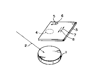
A laser beam (2) is applied to a target (1) of an
oxide superconductive material, to deposit atoms and/or
molecules which are scattered from the target (1) on a
first portion (4) of a substrate (3) under an atmosphere
containing oxygen for a start. Then, the substrate (3) is
moved to deposit atoms and/or molecules scattered from the
target (10) on a second portion, which is different form
the first portion (4) of the substrate (3), under the
atmosphere containing oxygen. At this time, the first
portion (4) is subjected to oxygen annealing. These
deposition steps are repeated until an oxide
superconducting film of a desired thickness is obtained.


French Abstract

Un faisceau laser (2) est appliqué sur une cible (1) en oxyde supraconducteur pour déposer des atomes et/ou molécules arrachés de ladite cible (1) sur une première partie (4) d'un substrat (3) sous atmosphère renfermant de l'oxygène au début. Puis, le substrat (3) est déplacé en vue du dépôt d'atomes et/ou molécules arrachés de la cible (10) sur une seconde partie du substrat (3), différente de la première partie (4), sous atmosphère renfermant de l'oxygène. € cet instant, la première partie (4) subit un recuit à l'oxygène. Ces étapes sont répétées jusqu'à obtention d'une couche d'oxyde supraconducteur d'épaisseur appropriée.

Claims

Note: Claims are shown in the official language in which they were submitted.


CLAIMS
1. A method of fabricating an oxide superconducting film
comprising:
a first deposition step of applying a laser beam to a
target of an oxide superconductive material for depositing
atoms and/or molecules scattered from said target on a first
portion of a substrate under atmosphere containing oxygen;
and
a second deposition step of moving said substrate for
depositing atoms and/or molecules scattered from said target
on a second portion of said substrate, being different from
said first portion of said substrate, under said atmosphere
containing oxygen, so that film formation is performed on
said second-portion of said substrate, while said first
portion of the substrate previously subjected to film
formation is oxygen-annealed to enable incorporation of
sufficient oxygen,
said first and second deposition steps being alternately
repeated.
2. A method of fabricating an oxide superconducting film in
accordance with claim 1, wherein said laser beam is a pulsed
beam having a frequency of at least 10 Hz.

Description

Note: Descriptions are shown in the official language in which they were submitted.


CA 02016028 1999-01-29
TITLE OF THE INVENTION
Method of Fabricating Oxide Superconducting Film
BACKGROUND OF THE INVENTION
E~ield of the Invention
The present invention relates to a method of
fabricating an oxide superconducting film, and more
particularly, it relates to a method of fabricating an
oxide superconducting film using laser ablation or laser
deposition.
Description of the Background Art
With recent development of laser units, there has
been proposed a laser deposition technique of applying a
laser beam to a target for vaporizing or sputtering the
target material and forming a film on a substrate (refer
to most Advanced Technology of Laser Processing
("Saisentan Laser Kako Gijutsu" in Japanese), published
May 22, 1989; editor Hiromichi Kawasumi; published by CMC
company, for example).
Such a laser deposition technique has the following
features:
(1) The film is generally formed at a high speed.
(2) The composition can be easily controlled.
In particular, laser ablation with an excimer pulse
laser beam, which has high energy density of at least 0.5
to 1 J/cm2, is highlighted as means for forming an
oxide superconducting thin film of Y-Ba-Cu-O, Bi-Sr-Ca-Cu-O
or the like, due to its capability of temperature reduction
_ .

2016028
" ,,
through photochemical reaction (refer to Appl. Phys. Lett.
53, 517 (1988) by C. C. Chang et al., for example).
It has been proved that the speed of film formation
by laser ablation is proportionate to the frequency of a
laser beam as used. If the frequency of a laser beam for
forming an oxide superconducting film of Y-Ba-Cu-O,
Bi-Sr-Ca-Cu-O or the like is simply increased, however, it
is difficult to incorporate oxygen, which must be
contained in such an oxide superconducting film, since the
speed of film formation is too high. When an oxide
superconductor contains insufficient oxygen, its critical
temperature TC is reduced. Thus, it is inexpedient to
increase the frequency of the laser~beam in order to
simply improve the speed of film formation.
In more concrete terms, it is possible to form a
Y-Ba-Cu-O film of about 1 to 2 ~ in thickness every pulse
by laser ablation with an ArF gas laser, for example.
Thus, a film of 18000 ~ to 36000 ~ in thickness can be
formed per hour with a laser beam of 5 Hz, for example.
However, if a film is formed with a laser beam of 10 Hz,
for example, sufficient oxygen cannot be incorporated into
the as-formed oxide superconducting film since the speed
of film formation is too high, although the amount of film
formation is theoretically doubled per unit time.
SUMMARY OF THE INVENTION

2~ ~ 6~ 28
Accordingly, an object of the present invention is to
provide a method of fabricating an oxide superconducting
film, which can incorporate sufficient oxygen even under a
high speed of film formation.
A method of the invention comprises:
a first deposition step of applying a laser beam to a
target of an oxide superconductive material for depositing
atoms and/or molecules scattered from said target on a first
portion of a substrate under atmosphere cont~;n;ng oxygen;
and
a second deposition step of moving said substrate for
depositing atoms and/or molecules scattered from said target
on a second portion of said substrate, being different from
said first portion of said substrate, under said atmosphere
cont~in;ng oxygen, so that film formation is performed on
said second portion of said substrate, while said first
portion of the substrate previously subjected to film
fonmation is oxygen-annealed to enable incorporation of
sufficient oxygen,
said first and second deposition steps being
alternately repeated.
BRIEF DESCRIPTION OF THE DRAWINGS
Fig. 1 is a perspective view illustrating the principle
of the inventive method of fabricating an oxide
superconducting film;

CA 02016028 1999-01-29
Fig. 2 illustrates relation between laser beam
frequency and film weight;
Fig. 3 illustrates relation between laser beam
frequency and critical temperature Tc; and
Fig. 4 is an plan view illustrating an exemplary mode
of movement of film forming regions achieved by moving a
substrate in Example of the present invention,
Referring to Fig.1, in more concrete terms, when a
laser beam 2 is applied to a target 1, film formation is
performed on a first portion 4 of a substrate 3, which is
opposed to the target 1. Such film formation is carried
out under an atmosphere containing oxygen. The substrate
3 is movable along arrows 5, 6, 7 and 8. Therefore, when
the substrate 3 is moved any direction, subsequent film
formation is performed on a second portion which is
different form the first portion 4 of the substrate 3. At
this time, oxygen annealing is carried out on the first
portion 4, which has been subjected to the film formation,
of the substrate 3 under the atmosphere containing oxygen,
so that sufficient oxygen can be incorporated into the
as-formed oxide superconducting film. Such deposition and
oxygen annealing are alternately repeated until an oxide
superconducting film having a desired thickness is
obtained.
According to the present invention, the frequency of
the laser beam is preferably selected to be at least
10 Hz.
Heretofore, the frequency of a laser beam has been
generally reduced below 10 Hz, in order to form an oxide
superconducting film of Y-Ba-Cu-O or Bi-Sr-Ca-Cu-O through
, . .

O ~ 8
laser ablation. In general, however, the frequency of
such a laser beam can be raised up to 60 Hz to 100 Hz, and
it is desirable to increase the laser beam frequency in
order to sufficiently effectuate the ability of the laser
unit and to increase the amount of film formation per unit
time.
According to the p~esent invention, the substrate is
moved after a portion thereof is subjected to film
formation of 50 ~, for example, to newly perform film
formation on another portion, while the portion previously
subjected to film formation is oxygen-annealed to enable
incorporation of sufficient oxygen. Thus, it is possibe
to use a laser beam having a frequency of at least 10 Hz,
for example, thereby sufficiently effectuating the ability
of the laser unit.
According to the present invention, therefore, it is
possible to form an oxide superconducting film at a high
speed using a high-frequency laser beam, without damaging
superconducting properties. Thus, the present invention
is particularly advantageously employed for the field of a
magnetic shield, a superconducting wire rod or the like,
which requires formation of a large amount of
superconducting films.
These and other objects, features, aspects and
advantages of the present invention will become more
apparent from the following detailed description of the
present invention when taken in conjunction with the
accompanying drawings.

CA 02016028 1999-01-29
.
DESCRIPTION OF THE PREFERRED EMBODMENTS
Before describing Example of the present invention,
the following reference example is presented:
Reference Example
A target of Yl Ba2Cu3O6 9 was used to perform laser
deposition with an ArF gas laser under an atmosphere
having oxygen pressure of 200 mTorr. An MgO substrate was
employed with a target-to-substrate distance of 40 mm and
a substrate temperature of 700~C. The fre~uency of a
laser beam having energy density of 1 J/pulse was varied
within a range of 1 Hz to 50 Hz, to carry out one-hour
film formation at some frequency levels within this range.
Figs. 2 and 3 show values of film weight and critical
temperature TC thus obtained.
The film weight is increased with the frequency level
as understood from Fig. 2, while the critical temperature
TC of the as-formed superconducting film falls below 77 K
~t frequency levels exceed~ O
-- 6 --

20160~8
.",,
result in no superconduction of the film in liquid
nitrogen.
Example of the present invention is now described.
ExamPle
Example of the present invention was prepared with a
target material, a laser, an atmosphere containing oxygen,
a substrate material, a substrate temperature and a
target-to-substrare distance which were similar to those
of the aforementioned reference example. As shown in
Fig.4, the size of the substrate was 60 mm x 40 mm, and
film forming regions were moved every second as ~ ~
... Energy density of the laser beam was
1 J/pulse similarly to the reference example, while its
frequency was 40 Hz.
The film weight measured after one-hour film
formation was 52 mg, and critical temperature TC was 90 K.
Comparing Example with the reference example, it is
understood that the critical temperature of the reference
example fell below 4.2 K at the laser beam frequency of 40
Hz to exhibit no superconduction in liquid nitrogen,
although its film weight was substantially identical to
that of Example. According to Example, on the other hand,
it is possible to attain a high critical temperature TC
since sufficient oxygen can be simultaneously incorporated

201~028
._ ,
into remaining portions when film formation is performed
on a certain portion.
Although the present invention has been described and
illustrated in detail, it is clearly understood that the
same is by way of illustration and example only and is not
to be taken by way of limitation, the scope of the present
invention being limited only by the terms of the appended
claims.

Representative Drawing
A single figure which represents the drawing illustrating the invention.
Administrative Status

2024-08-01:As part of the Next Generation Patents (NGP) transition, the Canadian Patents Database (CPD) now contains a more detailed Event History, which replicates the Event Log of our new back-office solution.

Please note that "Inactive:" events refers to events no longer in use in our new back-office solution.

For a clearer understanding of the status of the application/patent presented on this page, the site Disclaimer , as well as the definitions for Patent , Event History , Maintenance Fee  and Payment History  should be consulted.

Event History

Description Date
Inactive: IPC expired 2023-01-01
Inactive: IPC from MCD 2006-03-11
Time Limit for Reversal Expired 2001-05-03
Letter Sent 2000-05-03
Grant by Issuance 1999-07-20
Inactive: Cover page published 1999-07-19
Inactive: Received pages at allowance 1999-01-29
Pre-grant 1999-01-29
Inactive: Final fee received 1999-01-29
Letter Sent 1998-11-12
Notice of Allowance is Issued 1998-11-12
Inactive: Status info is complete as of Log entry date 1998-11-06
Inactive: Application prosecuted on TS as of Log entry date 1998-11-06
Inactive: Approved for allowance (AFA) 1998-10-29
Inactive: Adhoc Request Documented 1997-05-05
Deemed Abandoned - Failure to Respond to Maintenance Fee Notice 1997-05-05
Application Published (Open to Public Inspection) 1990-11-19
Request for Examination Requirements Determined Compliant 1990-05-03
All Requirements for Examination Determined Compliant 1990-05-03

Abandonment History

Abandonment Date Reason Reinstatement Date
1997-05-05

Maintenance Fee

The last payment was received on 1999-05-03

Note : If the full payment has not been received on or before the date indicated, a further fee may be required which may be one of the following

  • the reinstatement fee;
  • the late payment fee; or
  • additional fee to reverse deemed expiry.

Patent fees are adjusted on the 1st of January every year. The amounts above are the current amounts if received by December 31 of the current year.
Please refer to the CIPO Patent Fees web page to see all current fee amounts.

Fee History

Fee Type Anniversary Year Due Date Paid Date
MF (application, 8th anniv.) - standard 08 1998-05-04 1998-02-25
Final fee - standard 1999-01-29
MF (application, 9th anniv.) - standard 09 1999-05-03 1999-05-03
Owners on Record

Note: Records showing the ownership history in alphabetical order.

Current Owners on Record
SUMITOMO ELECTRIC INDUSTRIES, LTD.
Past Owners on Record
SHIGERU OKUDA
Past Owners that do not appear in the "Owners on Record" listing will appear in other documentation within the application.
Documents

To view selected files, please enter reCAPTCHA code :


To view images, click a link in the Document Description column. To download the documents, select one or more checkboxes in the first column and then click the "Download Selected in PDF format (Zip Archive)" or the "Download Selected as Single PDF" button.

List of published and non-published patent-specific documents on the CPD .

If you have any difficulty accessing content, you can call the Client Service Centre at 1-866-997-1936 or send them an e-mail at CIPO Client Service Centre.


Document
Description 
Date
(yyyy-mm-dd) 
Number of pages   Size of Image (KB) 
Description 1998-09-29 8 259
Claims 1998-09-29 1 28
Description 1999-01-28 8 261
Claims 1994-03-04 1 23
Abstract 1994-03-04 1 17
Drawings 1994-03-04 2 19
Description 1994-03-04 8 210
Representative drawing 1999-07-08 1 4
Commissioner's Notice - Application Found Allowable 1998-11-11 1 164
Maintenance Fee Notice 2000-05-30 1 178
Correspondence 1998-11-11 1 102
Correspondence 1999-01-28 4 159
Fees 1998-02-24 1 53
Fees 1999-05-02 1 48
Fees 1997-04-29 1 53
Fees 1996-04-30 1 47
Fees 1994-04-26 1 49
Fees 1995-04-23 1 48
Fees 1993-03-28 1 28
Fees 1992-03-04 1 29
Prosecution correspondence 1998-09-01 2 80
Examiner Requisition 1998-06-01 2 57
Prosecution correspondence 1996-09-17 1 43
Prosecution correspondence 1996-09-15 4 147
Examiner Requisition 1996-05-13 3 127
Prosecution correspondence 1993-05-06 6 236
Examiner Requisition 1992-11-17 1 64
Courtesy - Office Letter 1990-11-10 1 20