Note: Descriptions are shown in the official language in which they were submitted.
201~23
-` STRESS ISOLATED PLANAR FILTER DESIGN
~ .~
I I. FIELD OF THE INVENTION
.,
This invention relates to stress isolation of filter arrays, and
in particular to stress isolation of planar filter arrays in a filter
connector.
, II. DESCRIPTION OF RELATED ART
The use of filters in connectors is often critical to protect
sensitive components from transient currents and voltages which might
develop in a signal transmission cable due to electromagnetic and radio
10frequency interference. Such transients are generally high frequency
in nature, and therefore capacitive or tuned pi circuits are used to
shunt the transients to ground without affecting the primary signal
"l carried by the cable.
., Sophisticated ceramic technology has allowed such filters to fit
,~ 15within the connectors themselves. However, such ceramic filter arrays
are brittle and vulnerable to mechanical and thermal stresses on the
connector. Conventional arrangements for isolating the filter arrays
have proven inefficient, expensive, and overly complicated.
Consequently, a long-felt need exists for an efficient stress isolation
~:
.,; q~
~"
,..
:
~: . , ... - . :
- .: . . ~ . , . : . .
;`~' ' ~ ~ ' '' '' ' ,~ ', 1 , ' " ~ ~ " ' ",
20t6123
arrangement for ceramic filter arrays which is both
inexpensive and easy to assemble.
SUMMARY OF THE INVENTION
It is an object of an aspect of the invention to
y 5 provide improved means for isolating filter arrays from
mechanical and thermal stresses.
It is an object of an aspect of the invention to
provide impro-:^d stress isolation of planar ceramic
filter arrays.
It is an object of an aspect of the invention to
provide an improved multi-pin connector which includes
stress isolated planar capacitor filter arrays, and which
is easily assembled.
Finally, it is an object of an aspect of the
15 invention to provide an improved multi-pin connector
which includes stress isolated pi filters formed of
planar ceramic capacitor arrays and cylindrical ferrite
inductors, and which is easily assembled.
These objects are accomplished by providing
20 resilient gaskets which sandwich the planar filter arrays
to isolate them from shocks and stress.
These ob~Qcts are further accomplished by providing
a connector which includes planar filter arrays
sandwiched by resilient planar gaskets, and wherein the
25 filters are connected to ground via grounding springs
which serve to provide additional isolation for the
filter arrays from thermal mechanical stress.
Other aspects of thls invention are as follows:
An electrical connector, comprising a connector
30 housing and a substantially planar filter array
sandwiched between substantially planar resilient members
located within said housing, said planar resilient
members being arranged to isolate said filter array from
mechanical and thermal stresses to which the housing is
2016123
2a
subject, and further comprising grounding springs
arranged between said housing and said array to
electrically connect said housing with said filters, said
grounding springs being arranged to support said array in
said housing and to further isolate said array from
shocks.
: An electrical connector, comprising a connector
housing and a substantially planar capacitive filter
- array sandwiched between substantially planar resilient
members located within said housing, said planar
resilient members being arranged to isolate said filter
array from mechanical and thermal stresses to which the
. housing is subject, wherein said capacitive filter array
: is formed of ceramic dielectric material having a
plurality of electrodes embedded therein and a plurality
of apertures, said plurality of electrodes including pin
'. electrodes exposed at said apertures and electrically
connected to spring contact means for electrically
connecting said pin electrodes with connector pins, and
said plurality of electrodes also including grounding
, electrodes a portion of which extends around the
perimeter of said array, said grounding electrodes being
electrically connected to said housing by a grounding
spring arranged to support and further isolate said array
from mechanical and thermal stresses.
::;
:
~'
. . .. . .. . .
, , , ' ': , .
- ~ , , ,.-. .: . -.
20161Z3
BRIEF DESCRIPTION OF THE DRAWINGS
Figure 1 is a perspective exploded view of a connector according
to a first preferred embodiment of the invention.
Figure 2 is a cross-sectional side view of the connector of
figure 1.
Figure 3 is a schematic diagram of a capacitive filter circuit
, according to a second preferred embodiment of the invention.
3 Figure 4 is a side view depicting the manner in which the circuit
of figure 3 is mounted in a connector.
Figure 5 is a schematic diagram of a pi fil~er according to the
;i first preferred embodiment of the invention.
. Figure 6 is a side view showing the manner in which the filter of
figure 5 is mounted in a connector.
,.,
DESCRIPTION OF THE PREFERRED EMBODIMENTS
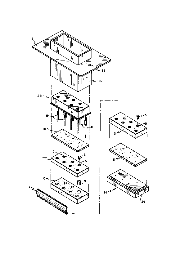
Figures 1 and 2 show a connector which exemplifies the principles
of the invention. The connector includes a housing shell 20,
preferably made of a conductive material such as aluminum. Other
suitable materials include metals or conductive plastics, and the
housing itself may be made of a single molded piece or may consist of
several parts.
The housing 20 includes a flange 21 which in turn includes means
such as screw holes 22 for securing the connector to an electronic
\ device. The shell 20 and connecting means 22 may be used to provide a
- ~ ground path for the filters in the connector as will be described
.
' :, '
....
,
.. .
-. :. ~ ... .~ :
~' ~ . :. ' -
2~ 23
below. In addition, the flange 21, combined with the conductive shell
20, provides increased electromagnetic interference protection.
Electrical signals pass through the connector along a path
provided by pins 8, which are configured as best shown in figure 4 to
provide receptacles for the insertion of male connector pins at one
end. It is, however, equally possible to configure pins 8 as male
connection pins in a manner well known in the art.
The pins 8 are inserted in receptacle 25 which fits inside
housing shell 20. Receptacle 25 is preferably made of a hard
dielectric material. Apertures in the receptacle receive the pins 8 on
one side and external connector pins on the other side in a
: conventional manner.
The opposite ends of pins 8 are inserted in a rigid insert 24
:~ which serves as an end cap for the connector housing 20 and as a means
by which a cable or other electrical device is electrically connected
to the connector pins. The means by which the cable is connected to
the connector pins forms no part of the present invention, but is noted
. that diverse such means are known to those skilled in the art.
, Elements 1 and 2 are planar ceramic capacitor arrays of the type
; 20 shown in more detail in figures 4 and 6. The use of the arrays shown
in figures 4 and 6 is not exclusive, however, it being possible to also
include arrays of discrete capacitors embedded in a solid insulative
material, or to use arrays of circuit elements other than capacitors.
As shown in figures 4 and 6, planar capacitor arrays 1 and 2 are
each formed of a plate of ceramic material including buried interleaved
conductive electrodes 5 and 6. The plate includes openings of
sufficient diameter to permit insertion of pins 8.
.
,- .
201~123
s
The pins 8 are connected to pin electrodes 5 by contact Cprings
: 3 inserted in the openings which serve to electrically connect pin
electrodes 5 with pins 8, snd also to secure pins 8 in the holes, while
providing mechanical stress isolation between the pins and the plates.
5Surrounding the perimeter of each capacitor plate is a ground
~ electrode electrically connected to alternate ones of the interleaved
-~ buried electrodes 6 as shown. Capacitor plates 1 and 2 are dimensioned
to fit within housing 20 with a slight clearance such that ground
`~ electrode 6 may be electrically connected to housing 20 by a grounding
lOspring 4, which also serves to isolate the capacitor array plates 1 and
2 from mechanical stresses on the housing shell 20.
The use of springs 4 permits secure electrical contact between
the ground electrode 6 and the housing shell 20 while also simplifying
, assembly by permitting a clearance between the plates and the housing.
~ 15Each of the components shown in figures l and 2 can be easily inserted
.~ in housing 20.
To further secure capacitor plates l and 2 in housing 20, and to
provide additional stress isolation with an extremely simple structure,
gaskets 15 and 16 are provided. Each gasket includes apertures for the
20insertion of pins 8. The ~askets are dlmensioned ~o securely fit
within housing shell 20.
Gaskets 15 and 16 may be made of any insulating material with
sufficient resilience to provide isolation from both mechanical and
thermal stresses. Silicon rubber has proved especially advantageous.
; 25Each of the elements 1, 2, 10, 15 and 16 shown in figure 1
, (element 10 will be described below) may be inserted into housing shell
:.,
.,20 without additional adhesives, although the use of adhesives in
: ,.
~,connection with the above-described structure is within the scope of
'.~
~s
.. , ::. ~ . :- .- . ... .
2016123
; 6
the invention. Insert 24 provides a convenient cap for securing the
gaskets and filter elements in the housing, and may include a shelf 26
as show~l to which adhesive can be applied to seal the connector.
Figures 3 and 5 show two different types of filters to which the
invention may be applied. The filter of figure 3 is a simple
capacitive filter implemented as shown in figure 4 by a planar
capacitor array electrically connected to ground through grounding
spring 4 and the housing 20. The pin electrodes 5 of the capacitor are
electrically connected to the pins 8 through contact springs 3, as
described above, and the capacitor array is directly sandwiched between
gaskets 15 and 16.
Thus, the capacitor array shown in figure 4 is completely
isolated from stresses in all directions, whether mechanical or thermal
in nature.
The pi filters of the embodiment shown in figures 5, 6 and also
.~ in Figures 1 and 2 include two capacitor arrays and cylindrical ferrite
inductors 11 which encircle pins 8 and are sandwiched between capacitor
` arrays 1 and 2. The cylindrical ferrite inductors 11 are embedded ina gasket 10, made of a resiliant material such as rubber, and which
. 20 serves to isolate both the cylintrical ferrite inductors and the
capacitor arrays from stresses and shocks.
The planar capacitor arrays continue to be completely isolated in
all directions, yet asqembly of the isolation structure simply involves
insertion of the inductors ll into gasket 10, and insertion into the
housing 20 of the remaining elements as shown.
As with the simpler capacitive filter embodiment depicted in
figure 4, each of the capacitive filter arrays of this embodiment are
connected to ground through a grounding spring 4 which may be formed of
2~)~6123
a single piece of stamped metal as shown or of two di.screte springs.
The type of conductive material used to form the grounding springs is
optional, of course. The inductors are preferably cylindrical ferrite
elements.
- 5 It will be noted that gaskets 10, 15 and 16 will also provide
protection for the planar filter arrays in respect to environmental
, degradation due to pollutants and moisture by forming a seal with the
housing 20 of the connector.
~, Those skilled in the art will appreciate that numerous
modifications of the invention are possible. For example, the
resilient planar gaskets of the invention may be used with filters
other than simple capacitive and pi filters, and in contexts other than
that of multi-pin connectors.
.~ The stress isolation provided by the gaskets will find
application in protecting diverse delicate components which may be
. placed in a connector. Of course, the housing shell need not be
rectangular as shown, but rather may be of any shape, and in particular
may be cylindrical, the corresponding planar filters and gaskets in
: that case also being round.
Consequently, it will be appreciated that the scope of the
invention should be limited solely by the appended claims.
: : . : , -
. . ., : . ~ .
::: - ,.: ...... . -