Note: Descriptions are shown in the official language in which they were submitted.
2 0 ~
EMBEDDED CONTROL TECHNIOUE FOR
DISTRIBUTED CONTROL SYSTEMS
BACKGROUND OF THE INVENTION
Field of the Invention
The present invention relates to distributed
control systems and more particularly to a control
technique wherein control information is embedded in
the information that is communicated between elements
of a system.
Description of the Prior Art
The trend in modern telephony equipment designs
has been to incorporate microprocessors as system
control elements. In most cases, such equipment must
support numerous replicated elements which provide
standard telephony services or interface standard
telephony signals such as DS1. Such elements are often
designed to minimize cost due to the impact of
replication and system cost. As a result, these
elements are often designed as non-intelligent elements
having simple, register-oriented control (ROC)
~;
.
. ' . ',
2 ~ f~,
interfaces; and which must be ¢ontrolled by a common
control element whose cost can then be effectively
distributed across the replicated elements.
A distributed control system architecture may use
multiple, distributed microprocessors (control
elements) which must communicate with one another and
with ROC interfaces in order to co-ordinate system
operations. These intelligent control elements often
communicate with each other using higher-level, message-
oriented control (MOC). A challenging aspect of such
architectures is to provide a mechanism for controlling
the numerous distributed elements, both intelligent and
non-intelligent, in a flexible, but cost-effective,
manner.
Non-intelligent elements which employ ROC must
receive control information from an intelligent control
element. The non-intelligent element normally responds
to control information immediately upon reception
thereof. Non-intelligent elements also produce
information which must be read and acted upon by the
control element. This information may fall into one of
two categories: urgent information which must be acted
upon quickly, and other information which may be
referenced on an as-needed basis or periodically
scanned at an appropriate rate.
,
- , ' .
~a~63a~
Intelligent elements which communicate via MOC
typically send messages in order to report significant
system events. Since the information carried in
messages may be urgent in nature, the receiving control
element must be notified upon arrival of a message in
order to promptly initiate message interpretation.
Also, since the number and frequency of messages
handled may be large, it is often important to minimize
the burden of message transmission and reception on the
control elements.
A common method of implementing MOC is by using
commercially available Data Link Control devices.
These devices are both costly and bulky, and separate
devices, or a separate channel of a multi-channeled
device, must be dedicated to each full duplex MOC
channel. Each such device requires interface circuitry
to synchronize its transmis6ion and reception. Also, a
Direct Memory Access (DMA) controller for each channel
is usually needed to free the control element from
handling each individual message character. While this
technique may be acceptable for a small number of
interconnected intelligent system elements, the cost
and physical space required may become prohibitive in
systems having a large number of elements.
20~3'~a ~
For non-intelligent ROC elements, there are a
myriad of techniques for implementing ROC, each one of
which is typically customized and optimized to the type
of element being controlled. In most cases where both
ROC and MOC are present, the ROC technique is different
and more primitive than the MOC technique. It is often
required that the control element explicitly request
information from the controlled element when needed.
If information is needed frequently in a system with
many replicated elements, the repetitious
request/response dialogue may represent a significant
overhead to the control element.
SUMMARY O~_THE INVENTION
The present invention will be described in the
context of a telephone system. However, it should be
noted that its application is general enough to be
extended to any distributed control system
architecture. ~n the following discussion, the term
'element' or 'system element' will be used as a
generalized reference to a sub-unit of a complete
system such as an individual printed circuit board
assembly. The term 'control element' refers to a
2 ~ ~ ~r~
system element which contains a controlling entity such
as a microprocessor.
In telephone systems, system elements are commonly
interconnected by means of serial data paths which
carry multiplexed voice and/or data information. Since
this network of data paths must exist to transport
voice/data information among the elements of the
system, it is desirable to use the same physical path
for control of the distributed elements in lieu of a
separate overlaid control network. This can be done by
allocating a small portion of the bandwidth, usually
referred to as a 'time slot', for the control
information. Since the control information is embedded
in the same signal path with the voice/data
information, it is referred to as an 'embedded' control
channel.
The present invention contemplates an embedded
control meahanism that can be used to transfer control
information transparently between two entities, one of
which is typically (but not necessarily) a control
element. The simplicity and flexibility of the
technique arises from the use of additional channel
bandwidth to transmit control information. The
technique allows the designer to greatly reduce the
complexity of the receiving devices.
2~3a.~
The format of control information communicated on
such a channel and the techniques for transmitting and
receiving such information are the subject of this
invention. A unique aspect of this technique is that
it may be used interchangeably for both ROC and MOC
devices and is equally efficient in either mode. An
additional advantage is that new elements may be added
to the architecture or existing elements may be
upgraded from ROC to MOC (or vice versa) without having
to anticipate in advance the ratio of ROC and MOC
elements that will be implemented.
Every unit of control information transferred by
the mechanism of this invention is accompanied by
control data which specifies how the information is to
be handled by the receiving element. This control data
may contain several fields which specify: 1) whether
the channel is idle or carrying valid information; 2)
the address or 'register number' into which the
information will be deposited at the receiving element;
3) whether the information is urgent in nature; and 4)
error detection information such as parity. Other
fields could exist in the control data if needed for
specific application: as, for example, if the urgency
of the information i9 to be prioritized, additional
bits could be provided in the field to establish a
-
''''
.:
.;
2 ~
priority rating. The above four mentioned fields will
be sufficient for a large class of applications and
shall therefore be used for illustration purposes in
the detailed description, which follows hereinafter.
It is not necessary that the control data and the
information be carried in the same channel. They may
be carried in separate channels, or even on separate
physical media, as long as their association is
preserved. For the sake of simplicity, it will be
assumed that both are carried in the same channel in
concatenated fashion. A channel may contain bits of
information representing the following: a valid data
indicator comprising a single bit indicating data valid
or not valid; an interrupt indicator which may comprise
a single bit alerting a microprocessor to interrupt and
service the message contained in the channel; a parity
bit for providing error detection; a field of bits
representing an address designating a destination
register or memory address in an intelligent device;
and an information data field for transparently
carrying the data between the system elements.
In ROC applications, the address field may be used
by the transmitting element, to randomly direct
information to control registers of a controlled
element. Likewise, the controlled element may return
. .
information, upon request or autonomously, to the
controlling element in randomly addressed fashion.
Alternatively a controlled element could routinely
transmit status information to its controller by
continually, or periodically, transmitting the
information in all of its registers sequentially. The
information could then be received and deposited in
'shadow registers' in the memory of an intelligent
controller where it could be referenced as needed by
the controller. In the event of some unusual or
otherwise significant event, the controlled element
could activate an interrupt field when transmitting the
register containing the pertinent information. When
received by the controller, the interrupt field could
be used to invoke the interrupt capability of the
microprocessor or other intelliqent device. If the
event was particularly critical, the information could,
in fact, suspend or supersede the normal sequential or
periodic transmission of routine status information by
the controlled element.
MOC applications are accommodated by virtue of the
transparent delivery of up to 2n message characters,
where n equals the number of address bits used. By
implementing a message transfer protocol which segments
and reassembles messages greater than m x 2n bits in
-8-
., - -" .:. .
:'' - , ` '. ' ~', . .
~ , , ~- .
2 ~
length, where m equals the number of bits in the
information data field, application software may
transmit messages of any length transparently. Message
segments could be brought to the attention of the
receiving processor by activating the interrupt field
of the last character transmitted in each segment.
This allows the receiving processor to efficiently
handle messages on a segment basis rather thar. a costly
character-by-character basis.
A key aspect of this invention is that no sequence
information need be retained by the receiving elements,
since the information is always transmitted with
explicit address tags. In an intelligent controller, a
specific region of memory should be mapped to each
channel carrying distributed control information. The
receive logic of the controller, upon receiving the
information, can easily derive the memory address into
which the information should be deposited by
concatenation of a base address, channel number (or
time slot) on which the information was received, and
the address tag received with the information. The
received information can then be deposited in the
memory by means of simplified direct memory access
(DMA), transparent to the processor, unless an
interrupt is indicated in the interrupt field. It is
_g_
2 ~
this simplifying feature that makes this technique
particularly attractive as an alternative to
conventional approaches involving replicated serial
communication devices and DMA controllers in
distributed systems with a centralized controller and a
large number of replicated elements.
A primary objective of the present invention is to
provide a distributed control system which does not
need a separate overlay of control paths.
Another objective of the present invention is to
provide a distributed control system that is compatible
for use with both ROC and MOC devices.
Another objective of the present invention is to
provide a distributed control system that is operative
with any combination of ROC and MOC devices.
Another objective of the present invention is to
provide a system which is transparent to the
information transmitted between elements.
Another objective of the present invention is to
provide duplex communication of control signals between
elements.
The above and other objectives and advantages of
the invention will become more apparent upon reading
the description of the invention in connection with the
drawings described below.
--10--
2 ~
DESCRIPTION OF THE DRAWINGS
Figure 1 is a block diagram illustrating a
distxibuted control system incorporating the embedded
control technique of the present invention.
Figure 2 illustrates the bit format used in the
control mechanism of the present invention.
DESCRIPTION OF THE PREFERRED EMBODIMENT
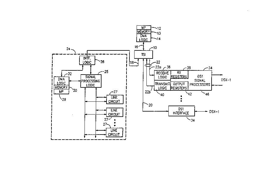
Figure l illustrates a distributed control system
incorporating the embedded control technique of the
present invention. The control system of Figure 1
diagramatically illustrates a device that could be used
in telecommunications. A time-slot interchanger (TSI)
10 is at the center of the system for distributing
speech, data and control information. A microprocessor
12 is shown having a plurality of registers which are
mapped into memory 13 by DMA logic 14. The
microprocessor is used to control the system and to
send control information to the various system
elements. The registers which reside in memory 13 are,
in effect, shadow registers to receive data from the
--11--
.: .
'
, .
- 20~3~
system elements and temporarily hold such data until a
time when the microprocessor can process the data.
A bidirectional serial data link 16 connects the
microprocessor 12 to the time-slot interchanger 10.
Link 16 comprises two unidirectional serial paths for
transmitting and receiving information.
The time-slot interchanger 10 is connected to a
number of system elements by serial data links 18, 20
and 22. Each of the serial data links comprises two
paths for unidirectionally transmitting and receiving
information. Link 22 is shown as two separate paths
22a and 22b for the purpose of simplifying the
description of the invention. Serial data link 18
connects the time-slot interchanger lO with an
intelligent terminal 24, which may be a control element
similar to microprocessor 12 used as shown in
con~unction with a line shelf used in a telephone
system. Intelligent terminal 24 may be connected to
additional system elements, not shown. Intelligent
terminal 24 includes interface logic 26 for separating
control information from voice and data signals which
are distributed to line circuits 27 via signal
processing logic 25 and a microcomputer including a
microprocessor 28, memory 30 and a direct memory access
(logic) 32.
.
. ~' , ~ , '
.
. -~ . . .
~ . . .
3 ~ ~
The time-slot interchanger 10 is further connected
by data links 20 and 22 to non-intelligent elements 34
such as DS1 terminals of a telecommunications system.
Link 22 is shown having path 22a connected to a receive
logic circuit 36, which distributes control information
based on an address, to receive registers 38, which may
be embedded in various application specific integrated
circuits (ASICs). In the present embodiment, the
receive logic 36, receive register 38, transmit logic
40, output register 42, and most of the DS1 signal
processing 46 are implemented in one such ASIC. It is
to be understood that the number of receive registers
38 provided within each ASIC may vary, depending on the
complexity of the ASIC and the control requirements.
Each ASIC is provided with one or more output registers
42 for assembling information to be returned to
microprocessor 12. The output registers 42 are
connected to path 22b of link 22 via transmit logic 40
for connection to microprocessor 12 through TSI 10 and
link 16.
The ASICs include an addressing and timing means
which may be used to initiate reading of the output
registers 42 during a particular period of time. The
address means may comprise counters connected to
receive a clock signal, said counters being adapted to
-13-
,
.
2 ~
provide an output for enabling the reading of the
registers 42 at a particular address or time slot, on
serial data link 22, associated with a particular ASIC
or a register within the ASIC.
As previously mentioned, serial data links 16, 18,
20 and 22 include two paths for transmitting and
receiving serial information. These serial data links
normally carry time multiplexed voice and/or data
information and are uniquely used in the present
invention to distribute control information between the
elements of a system. The control information may
include alarm, provisioning and control commands
between a control element such as microprocessor 12 and
the various systems elements such as the intelligent
terminal 24 or the DSl terminals 34.
The serial data links are time-division
multiplexed into a number of time slots as, for
example, thirty-two sequential time slots representing
a frame of information, with said frame being
repeated. These individual time slots are commonly
referred to as channels. The present invention relates
to the use of one or more of these channels to convey
alarm, provisioning or control commands for a
distributed control system. Thus, the control
mechanism of the present invention is embedded in the
-14-
~ ~ h ~ t~
data paths used to transport the voice and data
information of the telecommunications system.
The time slots, or channels, of the system in
which the present invention may be used, include data
or information in the form of words which may have any
arbitrary length: however, a length of 16 bits is used
in the described embodiment. The control mechanism of
the present invention is called a VI Channel, primarily
because one bit of data contained within the byte is
designated a V bit, or valid data indicator, while
another bit is designated an I bit, or interrupt
indicator.
The VI Channel bit format is illustrated in Figure
2, where the 16 bits are shown as being numbered from O
to 15, with O being the most significant bit and 15 the
least significant bit. The word of data is divided
into two fields, primarily an information field,
including bits O through 7 which provide eight data
bits and a control field comprising bits 8 through 15,
which includes the valid data bit V, the interrupt bit
I, a parity bit P and five address bits AO to A4 found
in bits 10 through 14, with bit A4 being in bit
position 10 and being the most significant bit.
--15--
".
'" '''''` ' " '
~-: .'` ' :,
. ' , . ` :
2 0 ~
The valid data indicator, bit V, indicates whether
the VI Channel is idle or is carrying valid data which
must be acted upon. The interrupt indicator I
indicates that the channel is signaling that the
information field contains information of an urgent
nature which should be acted upon immediately. The
parity bit P is a one-bit error detection field which
is established by the transmitting element and
evaluated by the receiving element to verify the
integrity of the entire byte. The address field AO to
A4 contains a unique address of a register in an ROC
device or of a location in a memory of a
microcomputerr such as memory 30 in the intelligent
terminal 24. For purposes of illustration, the address
field is shown as being five bits in length; however,
any length could be utilized as long as it is
compatible with the total available word length and the
bits of information needed in the information field.
In a similar manner, the information field is shown as
being eight bits long; however, any other convenient
length could be used that is compatible with total word
length.
The VI Channel is the alarm, provisioning and
communications channel between the controller and the
various elements of the system. The VI Channel format
is suitable for both message communication between
intelligent elements, such as control elements, and
register-oriented control for non-intelligent elements,
such as the DS1 terminals. The format described uses
half of the bandwidth for control and synchronization
purposes, while the remainder of the bandwidth is used
for data or information transfer. The format of the
VI Channel is completely transparent to the other
channels of the serial data link and therefore does not
interfere with the normal voice or data transmission.
The V bit indicates that the information being
transmitted is valid, while the I bit is used as an
interrupt for high-priority information. If the V bit
is not set, the contents of the VI Channel are
discarded and are not used by either the intelligent
terminal 24 or the non-intelligent DSl terminals 34.
In like manner, if a parity error exists, the contents
of the VI Channel will also be ignored.
The I bit in the VI Channel is used when messages
are being sent to an intelligent terminal, so that the
microprocessor may be interrupted to immediately act
upon the message being sent.
A key feature of the VI Channel mechanism is that
no sequence information need be retained by the
receiving element, since the information is always
.
transmitted with explicit address bits. In an
intelligent controller, a specific region of the memory
is mapped to each channel carrying distributed control
information. The receiver logic of the controller,
upon receiving the information, can easily derive the
memory address into which the information should be
deposited by concatenation of a base address, channel
number on which the information was received, and the
address bits received with the information. The
received information is deposited in memory such as 13
or 30 by means of the direct memory access (DMA) 14 or
32 respectively in a manner that is entirely
transparent to the processor, unless an interrupt (I
bit) is set, in which case the processor will be
interrupted at the first appropriate time to process
the data being received on the VI Channel. Note that
the DMA mechanism referred to here is not the
conventional DMA controller which must be capable of
sequencing memory operations by means of internal
memory address counters. The DMA logic used with this
invention is greatly simplified, requiring no internal
address counters or state memory. It is therefore
possible to implement DMA on a plurality of channels
inexpensively and in much less physical space. Thus,
the simplified mechanism of the present invention makes
-18-
.. .
, , . ~ , . , ' ~ . , ,
-
2 ~ ~ ~rh ~5 l7~ ~
it particularly attractive as an alternative toconventional approaches, involving replicated serial
communication devices and DMA controllers, in
distributed control systems with a centralized
controller and a large number of replicated elements.
For an understanding of the more detailed
operation of the present invention, reference should be
made to Figure 1. Microprocessor 12 generates a number
of messages or commands for various system elements.
These commands are inserted in VI Channels in serial
data link 16, with each channel containing a word as
shown in Fiqure 2, namely the information field and a
control field having an address and the V, I and P
bits. It is contemplated that serial data link 16 will
contain a plurality of VI Channels in each frame for
distributing control information. The TSI 10 receives
the VI Channels from link 16 and performs a grooming
function on the VI Channels along with the other
voice/data channels, distributing them to a plurality
of serial data links, such as 18, 20 and 22, in
accordance with its previously programmed channel
connection map. one or more VI Channels may be
serially transmitted on the transmission path 22a of
serial data link 22, where the logic element 36 decodes
the address and directs the byte to a register 38 in
--19--
...
2 ~ ~ ~ 3
accordance with the address contained within the VI
Channel word. If the VI Channel does not have the V
bit set, logic element 36 will ignore the word and will
not accept the VI Channel. In the transmit direction,
the I bit is not necessary when dealing with non-
intelligent system elements, since the VI Channel byte
is immediately loaded into a register if valid
information is indicated and the ASIC immediately
responds to the command.
When a message is sent to intelligent terminal 24,
the interface logic 26 will only accept the message
when the V bit is set in the VI Channel word. A
message may consist of a plurality of segments which
are accumulated in memory 30 by microprocessor 28.
Preferably the I bit will be set in the last character
of each segment, so that the processor 28 will handle
the message only after the complete segment is
available, and not on a character-by-character basis.
Messages being returned to the microprocessor 12
require that the I bit be set if immediate action by
the microprocessor is desired. Messages received on
the VI Channels by the microprocessor 12 will be
directed to shadow registers residing in memory 13,
where the messages will be stored until the
microprocessor polls the register at its convenience
-20-
, , . . :
.. ~,, - ~ . ' :
2 0 ~
for receiving the stored messages. However, upon
receipt of a message with the I bit set, the
microprocessor will be interrupted at the appropriate
time to act upon such message.
The various ASICs may have data to transmit back
to the microprocessor 12, and this data is loaded in
the output registers 42. The data could relate to
various signal status conditions or could be merely a
reflection of the received command, so that the
microprocessor can verify receipt of its last command.
Counters are provided with a clock signal, so that an
address may be generated. The counter provides an
enable signal during the appropriate time slot of the
VI Channel, so that the output register 42 for the
particular ASIC may be read to the serial data link 22
to transmit the return or reflected information in the
appropriate channel and with an appropriate address.
Thus, it can be seen that all communications
between syætem elements can be provided through the use
of VI Channels. Such communications include alarm,
provisioning and command functions. The VI Channel
mechanism provides a means to communicate between
system elements in a distributed control system, which
means does not need a separate overlay of control
paths. The VI Channel mechanism is uniquely compatible
-21-
'" "' .'
2 ~
with both ROC and MOC devices, and more particularly,
with any combination of such devices. The command
information is distributed transparently between system
elements and does not interfere with normal voice or
data communication.
-22-
,. " -, ., , , : ~
, - ,: . :
, : - , .. ~ :
, .,, :