Note: Descriptions are shown in the official language in which they were submitted.
-
201644~
TITLE OF THE l~v~Nl~ION
A T.tl~inAnce Signal/Color Signal Separating Circuit
and Noise Reduction Circuit Using a Comb Filter
BACKGROUND OF THE lNV ~ l ION
Field of the Invention
This invention relates to lllmin~nce signal/color
signal separating circuits and noise reduction circuits,
and more particularly, to lllmin~nce signal/color signal
separating circuits and noise reduction circuits using
comb filters in magnetic recording reproducing devices
such as video cassette recorders (hereinafter referred to
as VCR).
Description of the Background Art
A VCR has been proposed using a lH delay (DL) circuit
comprising one CCD (Charge Coupled Device), operating as a
comb filter during recording for separating an input video
signal into a lllmin~nce signal (Y) and a color signal (C)
(Y/C separation), and operating as a noise reduction
circuit during reproduction for removing the crosstalk
components in the reproduced color signal as well as
removing the small noise components in the reproduced
lllmin~ce signal, such 8s the one disclosed in ~apahese
Patent Laying-Open No. 59-107691 for example.
Y/C separation by a comb filter using a lH delay
circuit is well known, as disclosed in U.S. Patent No.
2016444
3,764,739. A color TV signal (hereinafter referred to as
video signal) of the NTSC system has the spectrum of
l~mi n~nce signal components and the spectrum of color
signal components alternately interleaved as shown
schematically in the frequency spectrum diagram of Fig. 1
to avoid beat disturbance on the screen. Generally, when
there is no difference between adjacent upper and lower
horizontal lines, that is, when there is line correlation,
lt~min~nce signal components are concentrated in the
vicinity of the spectrum of n times (n is integer) the
horizontal frequency fH (solid lines Y1), while color
signal components are concentrated in the vicinity of the
spectrum of (n + 1/2) fH (broken lines C). That is, Y
signal components and C signal components are mutually
lS frequency interleaved by (1/2) fH. On the contrary, when
there is difference between adjacent upper and lower
horizontal lines, that is, when there is no line
correlation, non-correlation components Y2 and Y3 of the Y
signal are generated respectively in the low frequency
region and the high frequency region of the complete band
of signal Y in a frequency interleaved relation with the
frequency multiplied output Yl of the horizontal frequency
(Fig. 1).
For example, in a VCR recording mode, a filter having
a comb type band-pass characteristic periodically repeated
` ~ -
201644q
in accordance with the repetition of the spectrum shown in
Fig. 1 is required to separately extract l~in~nce signal
components and color signal components from the input
video signal having such a frequency spectrum.
A filter having such a comb band-pass characteristic
is implemented by adding or subtracting an input video
signal (Y + C) and a signal delayed by lH by employing a
lH delay circuit, by means of a circuit shown in Fig. 3
for example. In the event of the above two signals being
added, a passing characteristic with the peak at nfH and
the valley at (n + 1/2) fH is realized as shown in Fig.
2(a) to pass the l~lrin~nce signal components Yl. On the
other hand, in the event of the above two signals being
subtracted, a passing characteristic with the valley at
nfH and the peak at (n +1/2) fH is réalized as shown in
Fig. 2 (b) to pass the color signal components C.
During a recording mode of a VCR, a Y/C separating
circuit using the above mentioned comb filter will extract
l~mi n~nce signal components in accordance wi~h the comb
type band-pass characteristic shown in the above Fig. 2
(a) with respect to the complete band of the ll~minance
signal. Therefore, the non-correlation components Y2 and
Y3 in the low and high frequency regions of Y in (1/2) fH
frequency interleaved relation with respect to Yl which is
the frequency multiplied output of the horizontal period
2016~4~
fH are not extracted in the low and high frequency regions
of the above mentioned complete band and will be excluded
from the lllmin~nce signal components. ?his eliminates the
~ in~nce signal variation between the upper and lower
lines, that is, in the vertical direction, resulting in a
problem of degradation in vertical resolution of the
picture on the screen.
A lH delay circuit used as a Y/C separating filter in
a recording mode will be used as a noise reduction circuit
during a VCR reproduction mode for removing the mixture of
low frequency converted color signal components from
adjacent tracks on a tape, that is, crosstalk, in the
reproduction system of the color signal. In addition,
this lH delay circuit will be used as a noise reduction
circuit for removing small noise components in a luminance
signal in the reproduction system of the lllmin~nce signal.
However, since such a noise reduction circuit will
suppress not only the noise components in the luminance
signal, but also the small signal components as noise,
there was a problem that the small signal components will
be decreased in the reproduced lll~in~nce signal.
Furthermore, generally in the reproduction mode, it
is regarded that conventional VCRs will compensate for the
missing reproduction signal, that is, will perform dropout
compensation using the lH delayed signal of the adjacent
- 2016~
horizontal period reproduced signal when the reproduced
signal is missing, i.e., when dropout occurs in a
horizontal period. However, the output of the lH delay
circuit constituting the above mentioned comb filter has
the phase of the color subcarrier 180 shifted with
respect to the missing reproduced signal to be
compensated. Therefore, the output of the lH delay
circuit may not be used for dropout compensation as it is.
SUMMARY OF THE lNV~NlION
Accordingly, an object of the present invention is to
prevent the degradation in vertical resolution of the
VCR ' s reproduced image.
Another object of the invention is to prevent the
decrease of small signal components in VCR' s reproduced
luminance signals.
Yet another object of the present invention is to
perform satisfy~g dropout compensation evén when dropout
occurs in VCR ' s reproduced signals.
Still another object of the invention is to provide a
lllmin~nce signal/color signal separating circuit that may
separate luminance signal components without removing
non-correlation components.
Still a further object of the invention is to provide
a noise reduction circuit that does not remove small
signal components in a luminance signal as noise.
201644~
A still further ob~ect of the invention is to provide
a noise reduction circuit for performing dropout
compensation using a lH delay circuit output of a comb
filter.
In summary, the present invention is configured so as
to extract the non-correlation components of a luminance
signal from the output of a subtraction circuit of a comb
filter to be added to a lllmin~nce signal component
provided from an addition circuit of the comb filter in a
lll~in~nce signal/color signal separating circuit using the
comb filter.
In accordance with another aspect of the present
invention, a l~l~inAnce signaltcolor signal separating
circuit is configured so as to previously enhance the
small signal components which will be suppressed by a
noise reduction circuit during reproduction to be added to
the ltl~in~nce signal component.
In accordance with another aspect of the invention, a
noise reduction circuit is configured so as to compensate
for dropout using the lH delayed reproduced lllmin~nce and
color signals by inverting the subcarrier phase of a color
signal of lH before when dropout occurs in the reproduced
signal.
Therefore, the main advantage of the present
invention resides in preventing the degration of vertical
- 20164~
resolution by adding non-correlation components to the
luminance signal component extracted by a comb filter to
compensate for lll~in~nce signal variation between
horizontal lines.
Another advantage of the present invention resides in
that the small signal components in l~lrin~nce signal will
not be suppressed as noise during reproduction, due to the
small signal components in lllmin~nce signal being enhanced
and recorded on a magnetic recording medium during
recording.
A further advantage of the invention resides in
satisfying dropout compensation using the output of a lH
delay circuit configuring a comb filter.
The foregoing and other objects, features, aspects
and advantages of the present invention will become more
apparent from the following detailed description of the
present invention when taken in conjunction with the
accompanying drawings.
BRIEF DESCRIPTION OF THE DRAWINGS
Fig. 1 is a schematic diagram showing the spectrum of
luminance signal component and color signal çomponent
Fig. 2 is a diagram showing the pass band
characteristic of a comb filter.
Fig. 3 is a schematic block diagram showing the basic
configuration of a comb filter.
- 20164i4
Fig. 4 is a block diagram schematically showing a
video signal recording system circuit of a VCR including a
Y/C separating circuit in accordance with one embodiment
of the invention.
Fig. 5 is a schematic block diagram with reference to
the Y signal separation portion in the Y/C separating
circuit of Fig. 4.
Fig. 6 is a block diagram schematically showing a
video signal reproduction circuit of a VCR including a
noise reduction circuit in accordance with one embodiment
of the invention.
Fig. 7 is a schematic block diagram showing the noise
reduction circuit of Fig. 6.
Fig. 8 is a circuit diagram showing an embodiment
that can be used as a Y/C separating circuit during
recording and a noise reduction circuit during
reproduction.
DESCRIPTION OF THE PREFERRED EMBODIMENT
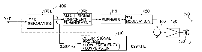
Fig. 4 is a block diagram schematically showing a
video signal recording circuit of a VCR including a Y/C
separating circuit in accordance with one embodiment of
the invention. Referring to Fig. 4, an input video signal
(Y + C) provided from a not shown signal source such as a
tuner is supplied to a Y/C separating circuit 100. The
applied signal is separated into a Y signal and a C signal
- 2016444
by a Y/C separating filter 100a comprised of the comb
filter previously mentioned in relation to Figs. 1-3.
The Y signal extracted from filter 100a has the small
signal components enhanced by a small signal component
S enhancement circuit 100b to be applied to an emphasis
circuit 110. The enhancement of this small signal
components will be explained in detail afterwards. The
extracted Y signal is subjected to emphasis process by the
emphasis circuit 100 and FM modulated by a FM modulation
circuit 120 to be applied to one input of an addition
circuit 140.
On the other hand, the C signal extracted by filter
100a is converted to a low frequency region signal of
629KHz from 3.58MHz by a color signal process circuit 130
and applied to the other input of addition circuit 140.
The Y and C signals mixed in addition circu-it 140 are
amplified by an amplifier 150 and recorded on a magnetic
tape 170 by a magnetic head 160.
Fig. 5 is a block diagram for schematically
explaining the operation of the Y signal separation
portion of the Y/C separating circuit 100 of Fig. 4. To
simplify the explanation, the illustration and explanation
corresponding to the small signal component enhancement
circuit 100b of Fig. 4 is here omitted, and will be
explained afterwards.
` - 20164~4
Referring to Fig. 5, the previously mentioned input
video signal (Y + C), or exactly (Yl + Y2 + Y3 + C)
including the non-correlation components of Y is provided
to the input terrin~l Tl of Y/C separating circuit 100.
The input video signal is directly applied to each one
input terminal of a subtraction circuit 5 and a addition
circuit 6, as well as to each of the other input terminal
of subtraction circuit 5 and addition circuit 6 after
being 1 horizontal period delayed by a lH delay circuit 1.
As previously mentioned, a color signal C and
non-correlation components Y2 and Y3 of Y, all having the
frequency spectrum of (n + 1/2) fH, are outputted from
subtraction circuit 5 to be applied to a band pass filter
(BPF) 8. BPF 8 extracts only the color signal component
C, and outputs it via terminal T3. On the other hand, a
luminance signal Yl having the frequency spectrum of nfH
is outputted from addition circuit 6. That is to say,
this luminance signal does not include the non-correlation
components Y2 and Y3 of the low and high frequency
regions, which means that degration of the resolution in
the vertical direction can not be avoided.
Therefore, the output (Y2 + C ~ Y3) of subtraction
circuit S is applied to a trap circuit 12 as well as to
BPF 8. The trap circuit 12 traps the C signal to output
the non-correlation components Y2 and Y3 of Y and applies
-- 10 --
- 20164~g
them to one input ter~in;tl of an addition circuit 18. The
output Yl of addition circuit 6 is delayed the delay time
of the above trap circuit 12 by a delay circuit 10, to be
applied to the other input terminal of addition circuit
18. As a result, the output Yl + Y2 + Y3 f addition
circuit 18 is provided as a llltninttlce signal via the
output ter~i n;tl T2 .
In the above manner of an embodiment of the present
invention, the non-correlation components Y2 + Y3 f Y are
added to the luminance signal component Yl of nfH
extracted by the comb filter. Consequently, the luminance
signal variation between lines is compensat,ed to prevent
the degration of the vertical resolution.
Fig. 6 is a block diagram schematically showing a
video signal reproduction system circuit of a VCR
including a noise reduction circuit in accordan,ce with one
embodiment of the invention. Referring to Fig. 6, the
video signal recorded on a magnetic tape 200 is reproduced
by a magnetic head 210 and amplified by an amplifier 220.
The ltl~in~nce signal component Y included in the output of
the amplifier 220 is extracted by a high pass filter (HPF)
230 to be FM demodulated by an FM demodulation circuit
240. The output of FM demodulation circuit 240 is applied
to a de-emphasis circuit 260 via a low pass filter (LPF)
250 to be de-emphasized. The output of the de c~rh;~sis
2016444
circuit 260 is applied to a noise reduction circuit 270.
In noise reduction circuit 270, Y signal has the small
noise components suppressed and dropout compensated to be
applied to a noise cancel circuit 280. The configuration
and operation of noise reduction circuit 270 will be
explained in detail afterwards. The noise cancel circuit
280 is provided which functions to reduce or cancel small
signal components in high frequency region of the input
signal so that the required S/N ratio can be assured.
Such noise cancellation can be performed by, for example,
extracting the high frequency small signal components of
an input through a HPF and a limiter and subtracting the
extracted small signal components from the input signal.
The Y signal having its noise components removed by noise
cancel circuit 280 is applied to one input of an addition
circuit 290. The output of the HPF 230 is also applied to
a dropout detecting circuit 340 which detects the dropout
of the reproduced 1l1~in~nce signal.
On the other hand, the color signal component C
included in the output of the amplifier 220 is extracted
by a LPF 300 and is converted to a high frequency region
signal by a high frequency region converting circuit 310
in accordance with the output of a voltage controlled
oscillator (VCO) 320. Then, it is applied to the noise
reduction circuit 270 via BPF 330. The signal C having
20164~
its crosstalk components removed by noise reduction
circuit 270 i8 applied to the other input of addition
circuit 290, as well as to VCO 320 to control the
oscillation frequency of VCO 320. From addition circuit
290, the reproduced video signal (Y + C) is outputted.
Fig. 7 is a block diagram for expl~ining the concept
of the operation of the noise reduction circuit 270 shown
in Fig. 6. Referring to Fig. 7, the reproduced ltlrinAnce
signal Y from the de-emphasis circuit 260 of Fig. 6 is
provided via ter~in~l T4 to one input terminal of a
subtraction circuit 19. The r,eproduced color signal C
from BPF 330 of Fig. 6 is provided via terminal T5 to one
input of an addition circuit 23.
The l-lrin~nce signal provided to ter~in~l T4 also
passes a delay circuit 20, a subtraction circuit 21, a
switch S4 and a trap circuit 22 to be applied to the other
input of addition circuit 23. Here, the lH delay circuit
1, delay circuit 4 and subtraction circuit 5 configure a
comb filter to extract the color signal component from the
output (Y + C) of addition circuit 23. This is provided
as a reproduced color signal C via BPF 8 and t~rrin~l T3.
Meanwhile, subtraction circuit 19 subtracts the output of
lH delay circuit 1 from the inputted reproduced luminance
signal to provide the color signal components and the
non-correlation signal components to trap circuit 12.
- 13 -
201644~
Trap circuit 12 removes the color signal band component
from the output of subtraction circuit 19 and applies it
as the noise component to the other input of subtraction
circuit 21 via a limiter 13 and an attenuator circuit 14.
In this way, the noise component is removed from the
lllmin~ce signal component Y applied to termin~l T4. The
output of subtraction circuit 21 is applied to a trap
circuit 22 via switch S4 to have its color signal
component removed. Then, it is outputted from terminal
T6, as well as being applied to the other input of
addition circuit 23 as a lllmin~nce signal with the noise
components removed. The delay circuit 20 is provided so
as to have a delay time equal to the delay time of the
non-correlation component detection system comprised of
trap circuit 12, limiter 13 and attenuator circuit 14.
When dropout occurs in reproduced signal, switches S4
and S5 are switched to select the signal path indicated by
dotted lines in response to a dropout detection signal
from the dropout detecting circuit 340 of Fig. 6. Then, a
reproduced luminance signal and a reproduced color signal
of lH before are selected and dropout is compensated.
That is, a luminance signal of lH before achieved by the
color signal component being trapped from the output of lH
delay circuit 1 in trap circuit 26 is outputted, through
switch S4 and trap circuit 22, from terminal T6, as well
- 14 -
2016~44
as being applied to addition circuit 23. Also, a color
signal of lH before extracted by HPF 25 from the output of
lH delay circuit 1 is provided to addition circuit 23 via
switch S5. As previously mentioned, the color signal will
have the phase of the color subcarrier 180 shifted from
- the original phase if dropout is compensated ~imply using
the lH delay signal. Therefore, in the embodiment of Fig.
7, the phase of the output of lH delay circuit 1 is
inverted at inverter 24 and only the color signal
component is separated at HPF 25.
In the above manner of one emboAi~ent of the present
invention, since the small signal components are enhanced
in recording, it will not be suppressed as noise
components during reproduction. Also, in the event of
dropout, the reproduced lll~in~nce signal and reproduced
color signal of lH before outputted from a lH delay
circuit constituting a comb filter are used to perform a
satisfying dropout compensation.
In the VCR of the invention, the Y/C separating
circuit 100 shown in Figs. 4 and 5 of recording and the
noise reduction circuit 270 shown in Figs. 6 and 7 of
reproduction can be configured to share an identical
circuit.
Fig. 8 shows such a circuit that can be used as a Y/C
separating circuit during recording, and as a noise
- 2ol6444
reduction circuit during reproduction. Referring to Fig.
8, the operation during recording will first be explained.
The same reference numbers as those of ~ig. 5 indicate the
same elements.
Firstly, an input video signal (Yl + Y2 + Y3 + C) is
provided to the input terminal Tl from a signal source not
shown. This is applied to each one input ter~in~l of a
subtraction circuit 5 and an addition circuit 6, to the
negative input terminal of a comparator circuit 11, and to
a lH delay circuit 1, via switch Sl which is switched to
the R side contact during recording. This lH delay
circuit l is comprised of one CCD and passes the complete
band signal components (Yl + Y2 + Y3
video signal. The output of lH delay circuit l is applied
to each of the other input terminal of subtraction circuit
5 and addition circuit 6, and to the positive input
terminal of comparator circuit ll via LPF 2, VCA 3 and
delay circuit 4. The comparator circuit ll controls the
gain of VCA 3 so that the signal level provided to each
input terminal of subtraction circuit 5 and addition
circuit 6 coincides with the signal level provided to each
of the other terminal thereof. The delay circuit 4 is
provided for fine-adjusting the delay time so that the
signal provided to each one input terminal of subtraction
circuit 5 and addition circuit 6 establishes lH time
- 16 -
2ol6444
difference with the signal provided to each of the other
terminal thereof. The output of subtraction circuit 5 is
applied to attenuator circuit 7 as a signal including the
C signal component and the non-correlation components Y2
and Y3 of Y, as explained in relation to Fig. 5, to have
the amplitude attenuated. Then, the signal (Y2 + C + Y3)
is applied to a band pass filter (BPF) 8 via switch S3
which is switched to a comb filter (C) side contact. Only
the color signal component C is extracted and provided
from terminal T3.
Meanwhile, the output (Y2 + C + Y3) of subtraction
5 is applied to trap circuit 12 via switch S2 that is
switched to the R side contact during recording. Trap
circuit 12 traps only the C signal component, as explained
in relation to Fig. 5, to output the non-correlation
components Y2 + Y3 f Y and applies them to one input
terminal of addition circuit 16. If the other input of
addition circuit 16 is not regarded, the ou-tput of trap
circuit 12 is applied to one input terminal of addition
circuit 18 via attenuator circuit 17. As explained in
relation to Fig. 5, the output of addition circuit 6 is
applied to the other input terminal of addition circuit 18
via attenuator circuit 9 and delay circuit 10 as a signal
including the lllmin~nce signal component Yl. Attenuator
2016~44
circuits 17 and 9 will attenuate the amplitude of the
input signal to a half.
As a result, the lllrin~nce signal (Y1 + Y2 + Y3)
including the non-correlation components of Y is provided
via output terminal T2 from addition circuit 18. The
delay circuit 10 is provided to have a delay time that is
equal to the delay time of the output of subtraction
circuit 5 to arrive at addition circuit 18 via trap
circuit 12, addition circuit 16 and attenuator circuit 17.
This is to avoid time difference between the two input
signals of addition circuit 18.
Next, the portion corresponding to small signal
component enhancement circuit lOOb of Fig. 4 is described.
The small signal component enhancement circuit is provided
to previously enhance the small signal components of Y
signal during recording to prevent the small signal
components in signal Y from being suppressed as noise by
the noise reduction circuit during the reproduction mode
of the VCR.
In Fig. 5, the non-correlation components Y2 + Y3 f
Y from trap circuit 12 has the amplitude limited by a
limiter 13 to be applied to an amplification factor
modifying circuit 4. The output of trap circuit 12 is
also applied to a non-correlation detection circuit lS.
During the period where the output of trap circuit 12
201644~
exceeds a predetermined level, non-correlation detecting
circuit 15 generates a control signal and applies it to a
gain control circuit 14. In response to this control
signal, gain control circuit 14 is disabled and the
s provision to the other input of addition circuit 16 is
ceased.
Also in response to this control signal, a gate
circuit 30 controls switch S3 so as to be switched to a
non-comb filter (NC) side contact. Therefore, not the
output of the above mentioned com~ type filter, i.e., the
output of subtraction circuit 5, but the color video
signal (Y + C) provided from terminal Tl is applied to BPF
8 via switch S3. More specifically, when non-correlation
of Y is detected, it is expected that non-correlation of
color signal is also generated. Therefore, in such a
case, the color signal component can not satisfactorily be
extracted by using a comb filter having a comb type
band-pass characteristic as shown in Fig. 2. As a result,
when the non-correlation occurs between two adjacent
horizontal lines, the supplied color signal is selected as
it is, instead of the output of the comb filter, to be
outputted as the color signal. The detail of gate circuit
30 will be described later.
On the other hand, during the period where the output
of trap circuit 12 does not exceed a predetermined level,
-- 19 --
- 201614~
non-correlation detection circuit 15 generates a control
signal and applies it to gain control circuit 14. Gain
control circuit 14 applies the output of limiter 13 to the
other input terminal of addition circuit 16 in response to
the applied control signal. Thus, the non-correlation
signal components Y2 and Y3 from trap circuit 12 are
enhanced and added to Yl signal by addition circuit 18.
This means that the small signal components of lll~in~nce
signal Y outputted from terminal T2 will be previously
amplified before recording. Also in response to this
control signal, the gate circuit controls switch S3 so as
to be switched to the C side contact, and the output of
the above mentioned comb filter, i.e., the output of
subtraction circuit 5 is applied to BPF 8 via switch S3.
In the above manner, the lllminAnce signal and the
color signal separated by the Y/C separating circuit are
respectively processed in accordance with the VHS record
format by each element 110, 120, 130, 140 and 150 of Fig.
4 to be further recorded on a magnetic tape 170 by a
magnetic head 160.
Referring to Fig. 8, the operation during
reproduction will be described. The same reference
numbers indicate the same elements of the reference
numbers in Fig. 7. The reproduced lll~in~nce signal Y
provided to t~r~in~l T4 from the de-emphasis circuit 260
- 20 -
2016444
of Fig. 6 is applied to the positive input of subtraction
circuit 19 for the detection of non-correlation
co...ponents, as well as to the positive input of
subtraction circuit 21 via delay circuit 20 that is
provided for timing with the non-correlation processing
system.
On the other hand, a lH delayed reproduced video
signal is applied to the negative input of subtraction
circuit 19 from lH delay circuit 1 via LPF 2 and VCA 3.
As a result, subtraction circuit 19 generates an output
including the non-correlation components of Y and the
color signal component and applies them to trap circuit 12
via switch S2 connected to the P side contact during
reproduction. In trap circuit 12, the C signal component
included in the lH del-ayed signal is removed, and only the
non-correlation components of Y are applied to the limiter
13 and non-correlation detection circuit 15. The
non-correlation components of Y having the amplitude
limited by the limiter 13 are applied to gain control
circuit 14. This gain control circuit 14 responds to the
contrQl signal output of non-correlation detection circuit
15 similar to the operation of the previously mentioned
recording to disable gain control circuit 14 during the
period where the non-correlation signal level is above a
predetermined level, and ceases the noise reduction
- 21 -
- 20164~ 1
operation. During this period, the gate circuit 30
controls switch S3 so as to be switched to select the
output of addition circuit 23, instead of the output of
the comb filter, i.e., the output of subtraction circuit
S. During the period where the non-correlation signal
level is below a predetermined level, the gain control
circuit 14 is enabled and the output thereof is applied to
the negative input of subtraction circuit 21 as the noise
components. As a result, a luminance signal component
having the noise components removed is provided from
subtraction circuit 21. This will be outputted from
terminal T7 via switch S4, as well as being applied to
trap circuit 22. Trap circuit 22 will remove the color
signal component included in the reproduced l~min~nce
lS signal and outputs it from terminal T6 as l~l~in~nce signal
Y. - .
This luminance signal Y is applied to one input of
addition circuit 23, while the reproduced color signal C
from BPF 330 of Fig. 6 is provided to the other input of
addition circuit 23 via terminal T5. The output of
addition circuit 23 is applied to the positive input of
subtraction circuit 5 configuring a comb filter, to the
negative input of comparator circuit 11, and to lH delay
circuit 1 via switch Sl switched to the P side contact
during reproduction. The output of lH delay circuit 1 is
- 2016~44
delayed for preciæely lH via LPF 2, VCA 3 and delay
circuit 4 to be applied to the negative input of
subtraction circuit 5. The color signal from subtraction
circuit 5 is attenuated by attenuator circuit 7 to be
outputted from terminal T3 via switch S3 and BPF 8 as the
color signal C.
Meanwhile, during the SP (standard play) mode, the
switch S3 is adapted to be controlled in response to the
detection of the non-correlation as described above.
However, during the EP (extended play) mode for example,
the switch S3 may be switched to select the C side contact
irrespective of detection of non-correlation since
crosstalk components from the adjacent tracks increase in
such EP mode. Therefore, the gate circuit 30 in provided
to control switch S3 in response to the control signal
from the non-correlation detection circuit 15 and tape
traveling speed (EP/SP) signal and the
recording/reproduction (REC/PLAY) signal.
Next, when the occurrence of dropout i~ reproduced
signals is detected at reproduction, the circuit
configuration is switched so that dropout compensation
will be performed using reproduced lllmin~nce signal and
reproduced color signal of lH before as the reproduced
lllmin~nce signal and reproduced color signal. In other
words, regarding the lllmin~nce signal component, switch S4
- 23 -
2016414
is switched so as to select the lH delayed signal having
the color signal component of the output from VCA 3
trapped at trap circuit 26 at the detection of dropout.
Dropout compensation is performed using this reproduced
luminance signal of lH before. Regarding the color signal
component, after the phase of the color subcarrier is
inverted by inverter 24, only the color signal component
is extracted by HBF 25 to be applied to one input of
addition circuit 23 through switch S5, as explained in
relation to Fig. 7. As a result, the phase inversion of
the color subcarrier will not occur even at dropout
compensation, leading to a satisfying dropout
compensation.
If the delay time of HPF 25 is half the period of the
color subcarrier, inverter 24 is not necessary. A delay
circuit for timing may be provided at the prior stage or
post stage of trap circuit 26.
Although the present invention has been described and
illustrated in detail, it is clearly understood that the
2Q same is by way of illustration and example only and is not
to be ~aken by way of limitation, the spirit and scope of
the present invention being limited only by the terms of
the appended claims.
- 24 -