Note: Descriptions are shown in the official language in which they were submitted.
SPECIFICATION
TITLE OF THE INVENTION
Optical Disk Reproducing Apparatus
BACKGROUND OF THE INVENTION
Field of the Invention
This invention relates to an optical disk reproducing
apparatus for reproducing digital data from a disk and, more
particularly, to such apparatus in which a continuous
playback output may be obtained even on the occurrence of
track jumps due to vibrations or the like.
Description of the Prior Art
In general, in a compact disk (CD), when a track jump
should occur during reproduction due to, for example,
vibrations of a pickup sy stem, reproduction is discontinued
or transiently interrupted to be restarted from some
different position, thus imparting a disagreeable feeling to
the listener or necessitating a redundant operation.
The prior art practice for reducing such track jump
has been to provide a mechanical damper in the CD player to
prevent the track jump due to vibrations, as disclosed for
example in the Japanese Patent Publication No. 62-69897
(1987).
However, when such mechanical damper is provided in the
CD player to prevent track jump, the CD player is more
complicated in structure and more expensive, while being
1
increased in size and weight and rendering future
retrofitting or remodelling difficult..
Moreover, when a strong impact is applied to the CD
player, such impact cannot be absorbed to cause the track
jump of the pickup despite provision of the damper.
While it is also proposed in to cope with the track jump
by corresponding signal processing as disclosed in Japanese
Patent Publication No. 63-1 77321 ( 1 988 ), the playback output
in this case becomes discontinuous because the playback
signal is not produced during track jump.
EiRIEF SUMMARY OF THE INVENTION
It is a principal object of the present invention to
provide an optical disk reproducing apparatus in which a
continuous playback output may be obtained even on the
occurrence of track jumps as a result of vibrations or the
like.
According to the present invention, there is provided an
optical disk reproducing apparatus in which an optical disk
is rotated at a first rotational speed on the basis of first
master clocks at the same time that digital data are
reproduced from said optical disk, comprising memory means
into and from which digital data detected from said optical
disk are sequentially written and read out, respectively,
track jump detection means detecting track jump of a light
spot during reproduction from said optical disk, resetting
2
means for resetting said light spot to a position just ahead
track jump, second master clock generating means for
generating second master clocks of a higher frequency than
said first master clocks, and control means f:or continuously
reading out digital data stored in said memory means on the
basis of said first master clocks on detection of track jump
by said track jump detection means, said control means
causing rotation of said optical disk at a second speed
higher than said first speed on the basis of said second
master clocks for a predetermined period after resetting of
said light spot by said resulting means for detecting digital
data from said optical disk for writing the detected digital
data in said memory means on the basis of said second master
clocks.
Thus, with the optical disk reproducing apparatus
according to the present invention, digital data detected
from the optical disk rotating at a first speed on the basis
of the first master clocks are sequentially written in memory
means on the basis of the first master clocks so as to be
read out and output after lapse of a time period not less
than a time period at least necessary for the light spot to
reset from track jump. Hence, on the occurrence of track
jumps by the light spot, digital data previously stored in
the memory means are continuously read on the basis of the
first master clocks to provide the playback output without
3
interruptions.
In addition, with the present optical disk reproducing
apparatus, the optical disk is rotated for a predetermined
time period after resetting of said light spot at a second
speed higher than the above mentioned first speed on the
basis of second master clocks having a higher frequency than
that of said first master clocks for detecting digital data
from the optical disk and writing the detected digital data
in the memory means on 'the basis of the second master clocks.
In this manner, the digital data read out from the memory
means during the time period necessary for resetting from the
track jump and hence depleted may be quickly replenished to
the memory means.
BRIEF DESCRTPTION OF THE DRAW2NGS
Fig. 1 is a block diagram showing the construction of a
CD player according to a first embodiment of the present
invention.
Fig. 2 is a block diagram showing the construction of a
memory section of the CD player shown in Fig. 1.
Fig. 3 is a time chart for illustrating the operation of
the CD player shown in Fig. 1 on the occurrence of a track
j ump .
Fig. 4 is a block diagram showing the construction of a
CD player according to a second embodiment of the present
invention.
4
Fig. 5 is a block diagram showing the construction of
the memory part of the CD player shown in Fig. 4.
DETAILED DESCRIPTTON OF THE PREFERRED EMBODIMENTS
By referring to the drawings, two illustrative
embodiments of the present invention applied to the CD player
will be explained in detail.
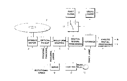
Fig. 1 is a block diagram showing a CD player. according
to a first embodiment of the present invention.
An optical pickup 1 directs a light spot on a compact
disk or CD 3, rotated by a spindle motor 2, to detect the
presence or absence of pits therein to generate RF detection
signals. These RF detection signals are processed in a
waveform shaping circuit 4 and thereby converted into digital
data which are transmitted to a digital signal processing
section 5 so as to be processed and converted into audio
data. These audio data are supplied to a memory section 6 so
as to be sequentially written and stored into a random access
memory (RAM) provided in the memory section 6. The stored
data are then sequentially read and transmitted to an analog
signal processing section 7 where they are converted by
digital to analog (D/A) conversion into analog signals and
output as stereo audio signals.
In the digital signal processing section 5, sub-codes of
digital data detected from CD 3 are detected and the
detection output is transmitted to a control section 8.
.'~.'~~3
Based on the detection output, the control section 8 monitors
the state of detection of the CD 3 to control a servo section
9 accordingly to apply a servo to optimize the rotational
speed of the spindle motor 2 or the state of tracking of the
light spot. An optimum focusing servo is applied in
accordance with focusing error signals, supplied from the
optical pickup 1 to 'the servo section 9.
The control section 8 outputs a mute signal which goes
high when digital data cease to be produced regularly from CD
3 and a play signal which goes low when the CD player is
operating in a playback mode. These mute and play signals
are applied to a non-inverting input and an inverting input
of an AND circuit 1 0 which then outputs to the memory section
6 a track jump detection signal which goes high when digital
data are not produced regularly during the reproducing
operation of the CD player, that is when a 'track jump has
occured.
The CD player is provided with two clock generators,
that is a usual clock generator 11 generating first master
clocks forming the basis of the normal reproducing operation
and a fast clock generator 12 generating second master clocks
having a frequency higher than in 'the first master clocks)
The master clocks output from these clock generators 1 1 , 1 2
are switchingly selected by a sw itching circuit 13 responsive
to control signals supplied from the memory section 6 before
6
being transmitted to the digital signal processing section 5
and thence to the memory section 6 and to the control section
8. The first master clocks from the usual clock generator 11
are pepetually supplied to the memory section 6 and thence to
the analog signal processing section 7 so as to form timing
clocks for D/A conversion.
Referring to Fig. 2, the memory section 6 includes a RAM
20 into and from which audio data supp7.ied from the digital
signal processing section 5 are written and read out,
respectively, as well as a write address controller 21, a
write address generator 22, a readout address generator 23,
an address selector 24 and an address comparator 25 for
generating write and readout address data supplied to RAM 20.
The write address controller 21 is supplied from the AND
circuit 10 with the above mentioned track jump detection
signal and controls the operation of the write address
generator 22 and the operation of the address selector 24 in
accordance with the track jump detection signals.
The first or second master clocks, supplied by way of
the switching circuit 13, are supplied to the write address
generator 22 from 'the digital signal processing section 5.
The write address generator 22 generates write address data
in timed relation with the master clocks which write address
data are transmitted to the address selector 24 and the
address comparator 25.
7
The first master clocks, generated in the usual clock
generator 11, are directly transmitted to the readout address
generator 23. The generator 23 generates address data in
timed relation with the first master clocks, which address
data are transmitted to the address selector 24 and to the
address comparator 25.
Responsive to control signals supplied from the write
address controller 21, the address selector 24 transmits the
address data supplied from the address generators 22, 23 to
RAM 20.
Responsive to write address data from address selector
24, the RAM 20 sequentially writes and stores audio data
supplied from the digital signal processing section 5 by way
of data input buffer 26. Responsive to readout address data
supplied from the address selector 24, the RAM 20
sequentially reads out and outputs the stored audio data to
transmit these audio data via data output buffer 27 to the
analog signal processing section 7. The RAM 20 is required
to have such a memory capacity that the audio data stored
therein can be continuously supplied to the analog signal
processing section 7 at least during the time necessary for
the light spot to reset from the track jump, as will be
explained in more detail later.
The address comparator 25 is responsive to the
difference between address data supplied thereto from the
8
address generators 22, 23 to transmit the control signal for_
the switching operation to the switching circuit 13.
Referring to Fig. 3, the operation of the above
described CD player will be explained for the case wherein
the track jump of the light spot has occurred during
reproduction from the CD 3.
The time period T1 shown in Fig. 3 shows the time period
when the CD 3 is being reproduced regularly. In this case,
the first master clocks generated in the usual clocJc
generator 11 are supplied to the digital signal processing
section 5 via switching circuit 13. Based on these first
master clocks, the CD 3 is rotated at a first speed (normal
playback speed) and, based on these first master clocks,
digital data are reproduced from CD 3.
Since the normal playback output is produced at this
time from CD 3 as shown at A in Fig. 3, a track jump
detection signal of a low (L) level indicating that a regular
playback operation is being performed as shown at B in Fig. 3
is supplied to the write address controller 21,
The write address controller 21 activates the write
address generator 22 when the track jump detection signal is
at the low level, as shown at C in Fig. 3. Since the first
master clocks are supplied at 'this time to both the write
address generator 22 and the readout address generator 23,
address data synchronized to each other are generated at the
9
address generators 22, 23. However, the readout address data
formed in the readout address generator 22 become the same
data as the write address data generated in the write address
generator 23 after a delay of a predetermined time longer
than the time period necessary for the light spot to reset
from the track jump.
When the track jump detection signal is at a low level,
the write address controller 2'1 controls the address selector
24, as shown at E in Fig. 3, in such a manner that the write
address data W generated in the write address generator 22
and the readout address data R generated at the readout
address generator 23 will be transmitted alternately to RAM
20.
In this manner, the audio data supplied 'to RAM 20 are
written into the address indicated by the write address data,
and are read out by the readout address data so as to be
output from RAM 20 after lapse of a time interval
corresponding to the del ay of the readout address data with
respect to the write address data.
When the CD player undergoes vibrations at time t~ in
Fig. 3 during reproduction from CD 3, and the light spot has
jumped over a track or tracks, by way of track jumps,
abnormalities are produced in the playback output from CD 3,
shown at A in Fig. 3. On detecting such track j ump of the
light spot from the abnormalities of the playback output, the
'I 0
i~.~a ~ ~~
controller 8 controls the servo section 9 to reset the light
spot to a position just ahead of the position at which the
track jump has occurred. Simultaneously, the controller 8
generates a high (H) level track jump detection signal
indicating the track jump of the light spot at the AND gate
as shown at B in Fig. 3 and transmits the high level
signal to the memory section 6.
When supplied with the above mentioned high level track
jump detection signal, the write address controller 21 of the
memory section 6 inactivates the write address generator 22
as shown at (in Fig. 3 to interrupt the generation of the
write address data. On the other hand, the readout address
generator 23 continues its operation, as shown at D in Fig.
3, on the basis of the first master clocks supplied from 'the
usual clock generator 11. The write address controller 21
controls the address selector 24, as shown at E in Fig. 3,
to discontinue the supply of the write address data to RAM 20
to supply only the readout address data to RAM 20.
For this reason, since the time t1 when the track jump
has occurred, the abnormal audio data transmitted from the
digital signal processing section 5 are not written into RAM
20. Only readout of the audio data previously written in RANI
before time t1 is performed in the usual manner.
When the light spot resets at time t2 in Fig. 3 to a
position just ahead of track jump, a normal playback output
11
~_'~.~~~~
starts again to be produced from CD 3, as shown at A in Fig.
3. This sets the track jump detection signal shown at B in
Fig. 3 to a low (L) level indicating that track jump has not
occurred. Thus the write address controller 21 reinitiates
the operation of the write address generator 22, as shown at
B in Fig. 3, to generate the write address data, while
controlling the address selector 24, as shown at E in Fig. 3,
to transmit the write address data and the readout address
data to RAM 20.
As described hereinabove, no audio data are written in
RAM 20 during the time period T2 since time t1 until time t2
when the track jump has occurred, and only readout of the
audio data previously stored in RAM 20 is performed. Hence,
at time t2, the readout address data approach to 'the above
mentioned write address data, so that there is but little
stock of the audio data written and stored in RAM 20.
In order to make for this the address comparator 25
compares the write address data with the readout address data
and transmits to the switching circuit 13 a control signal
which goes high as shown at F in Fig. 3 when the difference
between the write address data and the readout address data
is less than a predetermined value to cause the second master
clock from the fast clock oscillator 12 to be supplied to the
digital signal processing section 5.
In this manner, responsive to these second master
12
clocks, rotation of the spindle motor 2 and data processing
of digital data detected from the CD 3 are performed, such
that 'the CD 3 is ro'ta'ted at a second speed faster than the
above mentioned first speed, that is, the usual playback
speed, with the audio data being reproduced at an increased
speed from CD 3.
The above second master clocks are also supplied to the
write address generator 22, so that the write address data
are generated at higher than usual speed, such that the audio
data detected from the CD 3 are written in RAM 2 at an
elevated speed in response to these write address data. For
this reason, the audio data read out during the track jump
time T2 and thus depleted are replenished quickly in RAM 20.
When the difference between the write address data and
the readout address data is equal to a predetermined value at
time t3 in Fig. 3, the output of the address comparator 25 is
at the low (L) level, such that the first master clock output
from the usual clock generator 11 is again transmitted to for
example, the digital signal processing section 5 by means of
the switching circuit 13. Thus, since time t3, the various
parts operate in the same manner as during time interval T1
to reproduce the CD 3 under the normal state.
Meanwhile, during the time interval T3 since time t2
until time t3 when the audio data are reproduced from CD 3 by
the second master clocks, the first master clocks from the
13
~.~5~~
usual clock generator 11 are supplied to the readout address
generator 23, so that the audio data stored in RAM 20 are
read out in the usual manner. Similarly, the first master
clocks are supplied to the analog signal processing section
7, so that the audio data read out from the RAM 20 are
regularly converted into analog signals so as to be output
perpetually continuously.
It will be seen that, with the CD player to which the
present invention is applied, when the light spot has jumped
over a track or tracks, as a result of vibrations or the
like, the audio data may be continuously read out from RAM 20
to produce a continuous playback output. Moreover, by
reproducing the CD 3 at an elevated speed for a predetermined
time period T3 following reversion of the light spot to a
position just ahead of the track jump, audio data may be
quickly replenished in the RAM 20 in readiness for the next
track jump. For this reason, perpetually consecutive audio
signals can be continuously output even when the CD player is
employed under the conditions in which track jumps are likely
to occur frequently.
Fig. 4 shows in a block diagram a CD player according to
a second embodiment of the present invention and Fig. 5 shows
in a block diagram the construction of the memory section 6
in the CD player shown in Fig. 4.
Tn Figs. 4 and S, the same or equivalent parts as those
14
shown in Figs. 1 and 2 are indicated by the same numerals as
in Figs. 1 and 2, and only the parts or components different
from Figs. 1 and 2 are explained for avoiding redundant
description.
With the CD player of the first embodiment, the track
jump detection signal is generated from the play signal and
the mute signal output from the controller 8 so as to be
supplied to the memory section 6. However, with the CD
player of the present second embodiment, a detection signal
of the track jump of the light spot and the detection signal
of the subcode of digital data detected from CD 3 are
supplied from the controller 8 to the memory section 6, as
shown in Fig. 4. An address memory 28 is included in the
memory section 6, as shown in Fig. 5, so as to be supplied
with the subcode detection signal.
The address memory 28 is adapted for latching write
address data output from the write address generator 22, with
the subcode detection signal as the latch timing signal.
Hence, in case of the track jump of the light spot, the write
address data just ahead of track jump when the subcode ceases
to be detected are stored in the address memory section 28.
The write address data just ahead of track jump are supplied
to the write address generator 22 by means of the write
address controller 21, such that, when the light spot reverts
from the track jump and the write address generator 22 is
again actuated, audio data start to be output from this write
address on.
In this manner, after the light spot reverts from the
track jump, audio data from the digital signal processing
section 5 are written from the address just ahead of the
preceding track jump, so that no unusual data are left in RAM
20 even if the interruption of the operation of the write
address generator 22 is delayed.
With the optical disk reproducing apparatus of the
present invention, digital data reproduced from the optical
disk are written in memory means so as to be read and output
after lapse of a time interval not shorter than a time period
necessary for the light spot to reset at least from track
jump. Henr.e, on occurrence of a track jump, a continuous
playback output may be obtained by continuously reading out
and outputting digital data from the memory means.
In addition, with the present optical disk reproducing
apparatus, the optical disk is reproduced at an elevated
speed for a predetermined period after reversion of the light
spot to a position just ahead of the track jump, so that
digital data may be quickly replenished in the above memory
means in readiness for the next track jump,
With such optical disk reproducing apparatus, a
perpetually continuous playback output may be obtained even
on occurrence of a track jump as a result of vibrations or
16
the like so 'that the vibration damping mechanism may be
simplified. The optical reproducing apparatus may be
advantageously employed with portable CD players or CD
players mounted on vehicles where severe vibrations are
encountered.
17