Note: Descriptions are shown in the official language in which they were submitted.
2 ~ 1 7 0 9 9
File No. 10577-180 DNS/MEW/jh
SEOUENTIAL PARITY CORRECTION
FIELD OF THE INVENTION
This invention relates to a sequential parity
correction apparatus. More specifically, this invention
relates to an apparatus and method of correcting parity
errors in a fault tolerant computer system.
BACKGROUND OF THE INVENTION
In standard computer systems, errors in data
processing can occur which will halt operation of the
computer system. These errors can be caused by, among
other things, erroneous data or erroneous microcode.
Both data and microcode are stored in memory devices
which occasionally fail, and faulty information will be
accessed from the memory device. To help ensure the
integrity of data, additional data called a parity bit
is added to stored information. Generating and checking
parity data are well known in the computer art. If a
parity check indicates that faulty data exists,
conventional computers generate an error indication, and
operation is halted until an operator intervenes. Some
systems have the capability of correcting single bit
errors, but cannot correct double bit errors in a word.
To overcome this difficulty, as well as provide
other benefits, fault tolerant computers were developed
which use "correctable" sources for some of the data, as
well as error correction hardware and algorithms to
correct errors. A correctable source refers to the
ability of the computer to identify and correct faulty
data stored in the device without the computer shutting
down or requiring operator intervention. One
implementation of fa~lt tolerance is directed to data
stored in a random access memory (RAM). A system was
developed by which faulty data accessed from the RAM
~ ~ 2~7Q99
could be detected and corrected, without appreciably or
adversely affecting the performance of the computer.
A time-critical path refers to a data path which
is the slowest, or among the slowest, with respect to a
particular operation sought to be implemented and
measured. The importance of a data path being
denominated a time-critical path, is the realization that
in operating a computer it does not matter whether other
parts of the machine operate at very fast speeds. The
overall system cannot operate any faster than its slowest
path. Therefore, to enhance computer capabilities, time-
critical paths are analyzed and methods are sought to
increase their performance.
The paths which data takes from its storage in
RAM and its eventual use by a processing device are
traditionally two such time-critical paths. The first
path is from the RAM to the register. The second path
is from the register through the ALU. Actually, the ALU
is a separate time critical path. Typically, data in the
RAM is accessed and temporarily stored in a RAM data
register before the data is used. By use of a RAM data
register, the effective time required to address data and
use the data was reduced as data could be accessed from
storage while a processing device was busy. The addition
of a data register was crucial to increase the overall
speed of a computer since data could be stored in the
register in anticipation of its use and therefore
accessed from the register much faster than directly out
of the RAM.
Fig. 1 shows a prior art fault tolerant
implementation which used a parity checker and generator
in a data path between a RAM data register and a ALU. In
a memory storage device, such as a RAM array 10 which is
correctable, there is stored: a data word 12, parity
data 14 for the stored data word 12, and $pare memory 16
is provided in the storage device to allow the RAM to be
self-correcting. A processing device 18, herein depicted
201 7099
3 64157-324
as an ALU, executes instructions and process data accessed from
the RAM array 10. A RAM data register 20 enhances the access time
of the ALU 18 to data stored in the RAM array 10. A data path 30
carries both the data word 12 and the parity data 14 associated
with the data word 12. The data may be carried either serially or
in parallel, as is well known to those skilled in the art.
A parity checker 32 and parity generator 34 are
interposed between the RAM data register 20 and the ALU 18 to test
the data word 12 accessed from the RAM array 10 before it is
processed by the arithmetic logic unit (ALU) 18. It is understood
that in practice, a parity generator 34 and a parity checker 32
often share much of the same circuit elements. They are shown
separated due to their functional distinctions and to ease
understanding. A data path 40 provides the data word 12 and the
parity data 14 to the parity checker 32 from the RAM data register
20. Upon detection of an error, a control circuit 42 is provided
an error signal from the parity checker 32 via a path 44 which
pauses downstream registers while the parity generator 34
generates the correct parity data 50 for the data word 12. Only
the data word 12 is supplied to the parity generator 34 on data
path 52 to allow the parity generator 34 to generate good parity
for all data accessed from the RAM array 10, whether it is
actually faulty or not. Thus, a data path 54 will provide the
data word 12 and the generated parity 50 to the ALU 18. When the
generated parity 50 is ready, the control circuit 42 allows the
processing of the data word 12 to continue. Then the ALU 18 may
perform an instruction on the data word 12, with the output of the
ALU 18 appearing on a data path 56 to be sent to other registers
,.
= =
201 7099
3a 64157-324
and tested by other parity checkers. The control circuit 42 also
initiates an error correction algorithm to correct the faulty data
stored in the RAM, and to purge the system of erroneous data and
calculations.
2017099
The prior art sequential parity correction
system, while acceptable for many applications, has the
drawback that the parity checker 32 and parity generator
34, a relatively slow device, are in a critical path with
the ALU 18. Therefore, the ALU 18 may not begin
processing the data until after the parity checker 32 has
determined whether a parity error has occurred, and the
parity generator 34 has generated correct parity 50.
Usually, the data will be good, which means a needless
delay has been added to the time-critical data path
described above. The delay arises because the parity
generator 34 generates correct parity 50 for each and
every data word 12 regardless of whether an error has
occurred.
As discussed above, ALU ' s contain a time critical
path. Some prior art systems had the practice of
following an ALU with a parity generator whereby parity
data for a result calculated by the ALU would have parity
associated with it by generation of parity for the
result. The method had two disadvantages: 1) a slow
device was put in a time critical path; and 2 ) if the
result was faulty, correct parity would be generated for
the faulty data and downstream registers would not detect
an error. To improve performance, parity prediction was
25 implemented. Parity prediction is a method of
calculating a data word's parity for the result
calculated by the ALU. Parity prediction uses a separate
circuit in parallel with the ALU to calculate the parity
of an ALU result of an operation on data words A and B.
The parity prediction uses A, B, and the parity for A and
B to predict what the parity will be for the result of
the operation on A and B. Therefore, the predicted
parity is independent of the correct operation of the ALU
as it is not based on the result. The prediction
circuitry is outside any time critical path of the ALU
and will allow downstream parity detectors to determine
if a failure occurred.
i,~ 7 Q 9 9
There may be other time critical paths which are
slower still; therefore for certain applications the
error correcting system of the prior art would be
functional and useful.
.. . .
- SUMMARY OF THE INVENTION
~ The .present~.invention~-enhances .the performance
of computing=systems while preserving the fault-tolerant
characteristics of the.correction system. With computing
systems, there is always the desire to increase overall
system speed. To increase speed, the time critical paths
are analyzed and ways are sought to increase the
performance of.all such paths. The present invention is
an improvement in the speed and efficiency of sequential
parity correction in the time-critical path between a
correctabl.e memory source and a processing device
utilizing .the..data.. The invention.utilizes a parity
checker and.generator, but these are taken out of the
time-critical.path between-the RAM.data register:and the
. kF.U.~nd placed~-in parallel-tQ the.ALU .data path. -The
parity checker tasts the-data.-input into the ALU without
interfering:~-with the-ALU's operation. That is, while the
testing. is being performed, the ALU is executing its
instructions and processing the data. If- the. data is
.. good, processing continues and no delay has been added to
the data path for parity checking.
.. .. In the.unlikely event that faulty data has been
detected, the parity checker generates an error signal
indicating that faulty data exists. This error signal
is input to. a control circuit which performs several
functions. First, all downstream registers which may
pass the data to other parity checkers to detect the
faulty data are temporarily "paused." This prevents any
downstream error detectors from freezing the system.
Next, the ALU is commanded to pass, unchanged, the faulty
data to the output. The data is combined with new parity
data which has been generated by a parity generator
20~ 7099
6 64157-324
connected to the parallel parity checker. This generated parity
data is now correct for the data, though the data itself may be
faulty, and is substituted for the data in the RAM data register
to be re-input into the ALU.
Once the data is substituted, which is a relatively fast
operation, the control circuit allows the ALU to process the new
data, and downstream registers are permitted to resume normal
processing. The present invention has a further advantage in that
the actual algorithm used to correct the data is unchanged from
that used in the prior art.
The error correcting circuitry and method are not part
OL this disclosure. Il musi ~e appreciated that an error signal
may be generated by the parity checker 32 upon either of two
conditions. The first is that the data word 12 is incorrect and
its parity data 14 is good. The second condition is that the
parity data 14 is faulty, while the data word 12 is correct. The
present invention does not discriminate between these two fault
conditions.
According to a broad aspect of the invention there is
~0 provided a data processing computer, including:
a memory device for storing data and associated parity
information;
a temporary memory operatively coupled to the memory device
for temporarily storing data and its associated parity information
retrieved from the memory device,
a processing device, operatively coupled to the temporary
memory, for processing the data temporarily stored in the
temporary memory and providing the result at a data output
201 7099
6a 64157-324
terminal;
a parity checker, operatively coupled to the temporary memory
in parallel with the processing device, for testing the stored
data with its associated parity information, and generating a
signal indicating the status of the test;
a parity generator, operatively coupled to the parity
checker, for generating correct parity for the stored data and
providing the result at a parity output terminal;
a multiplexer having a first multiplexer input terminal
coupled to the memory device, a second multiplexer input terminal
coupled to the processing device data output terminal and the
parity output terminal, and a select terminal;
a control circuit, operatively coupled to the parity checker
and responsive to the status test signal;
the control circuit operating in response to a failed parity
indication to pause data paths coupled to the processing device
data output terminal, to cause the processing device to pass the
stored data directly to its data output terminal, and to select
the second multiplexer input terminal; and
the control circuit operating in response to the absence of a
failed parity indication to select the first multiplexer input
terminal;
such that in the event of a failed parity indication, the
correct parity is substituted for the associated parity
information and input along with the stored data to the temporary
memory for subsequent input to the processing device.
According to another broad aspect of the invention there
is provided in a computer having a memory to store data composed
20~ ~o~q
6b 64157-324
of data words and associated parity for the data words, a
temporary storage device coupled to the memory for temporarily
storing data words read from the memory, a processing device
having a data input port coupled to the temporary storage device
and a command port for causing the processing device to pass a
data word at its input to an output, and an output data path from
the output of the processing device, a parity correction apparatus
comprising:
a multiplexer operatively interconnected between the memory
and the temporary storage device, the multiplexer having a first
data input coupled to the memory, a second data input, an output
coupled to the temporary storage device, and having an address
select to determine which of the first and second data inputs is
routed to the output;
a parity checker operatively coupled to the temporary storage
device in parallel with the processing device to test the data
word being read from the temporary storage device against the
associated parity such that the parity checker will generate an
error signal upon detection of a parity error;
a parity generator operatively coupled to the parity checker
to generate correct parity for the data word read from the
temporary storage device, the generator outputting a correct
parity on a data path operatively coupled to the second input of
the multiplexer;
means for combining the correct parity and the data word
passed from the processing device onto the data path operatively
coupled to the second input of the multiplexer; and
a control circuit operatively coupled to the parity checker,
A
20 1 7099
6c 6415~-324
the processing device, and the multiplexer, the control circuit
responsive to the error signal to generate a first signal, a
second signal, and a third signal, such that the first signal
pauses the further processing of the data word by a downstream
register, the second signal operatively coupled to the command
port of the processing device to pass the data word unchanged, and
the third signal coupled ~o the address input of the multiplexer
to select the second input in lieu of the first input when the
error signal is present.
According to another broad aspect of the invention there
is provided in a data processing system having a memory system
operatively coupled to a processing device, a sequential parity
correction circuit comprising:
a multiplexer having a first input operatively coupled to the
memory system and an output operatively coupled to the processing
device;
a parity checker operably coupled to the output of the
multiplexer, and in parallel to the processing device, to test the
parity of a data word input to the processing device, the parity
checker generating a signal indicating the condition of the parity
for the data word;
a parity generator operably coupled to the parity checker and
responsive to the signal generated by the parity checker to
generate and output correct parity for the data word input into
the processing device when the parity checker signal indicates
that a parity error has occurred, the output of the parity
generator operably coupled to a second input of the multiplexer;
and
201 7099
6d 64157-324
a control circuit operably coupled to the parity checker and
responsive to the signal generated by the parity checker when the
signal indicates that a parity error exists,
the control circuit generating a first signal, the first
signal operatively coupled to the processing device to cause the
data word input to the processing device to be passed to the
output of the processing device, the processing device output
operatively coupled to the second input of the multiplexer,
the control circuit generating a second signal, the second
signal operatively coupled to registers in the data processing
system to temporarily pause processing so that the detected parity
error is prevented from triggering any downstream error detectors,
and
the control circuit generating an address signal, the address
signal operatively coupled to an address input of the multiplexer
such that data at the ~irst input to the multiplexer is selected
and passed to the output of the multiplexer except in those
instances when the signal from the parity generator indicates that
a parity error has occurred and then the data input into the
second input of the multiplexer is selected and passed to the
output of the multiplexer.
According to another broad aspect of the invention there
is provided in a data processing system having a memory system
coupled to provide a data word and an associated parity word to a
processing device, a parity substituting apparatus comprising:
means for parallel testing of parity for the data word and
associated parity word input into the processing device to provide
an error signal indication of a parity error;
,. ~f
201 709q
6e 64157-324
means for generating another parity word for the data word
input to the processing device without regard to the correctness
of such data word, in parallel with the processing device,
means, responsive to the error signal, for substituting the
another parity word with the data word then input to the
processing device in place of the associated parity word, and
applying the another parity word and the data word to the
processing device; and
means, responsive to the error signal, for pausing downstream
registers from additional processing of data from the processing
device until the association of the data word and another parity
word has occurred.
According to another broad aspect of the invention there
is provided in a data processing system having a memory system
operatively coupled to an ALU, a parity correction apparatus
comprising:
means for parallel testing of parity for a data word input to
an ALU to provide an error signal indication of a parity error;
means for generating correct parity for the data word input
to the ALU, in parallel with the ALU;
means responsive to the error signal, for associating the
correct parity with the data word and substituting the associated
correct parity and data word to the ALU; and
means, responsive to the error signal, for pausing the
processing of data downstream from the ALU until the association
and substitution of the data word and correct parity has occurred.
According to another broad aspect of the invention there
is provided a method for correcting parity in a data processing
~ F.
20 1 7099
6f 64157-324
system having a source memory for storing a plurality of data
words and parity data associated with each of the plurality of
data words, and a processing device to operate upon each of the
data words se~uentially read from the memory, the method
comprising the steps of:
asserting a parity error from parallel testing the parity of
each of the data words input to the processing device;
generating, in parallel to data processing by the processing
device, another parity for the each of the data word input to the
processing device without regard to the correctness of such data
word;
responding to assertion of the parity error by associating
the another parity with the input data word and inputting the data
word back to the processing device; and
pausing the downstream registers from additional processing
of data until the another parity has been associated with the data
word when the parity error is asserted.
According to another broad aspect of the invention there
is provided a method for substituting parity data in a data
processing system having a source memory for storing a plurality
of data words each having associated parity data, a temporary
storage device coupled between the memory and an arithmetic-logic-
unit (ALU), the method comprising the steps of:
parallel testing each of the plurality of data words input
into the ALU against the associated parity data;
generating an error indication of failed parity,
generating, in parallel to ALU data processing, another
parity data for each of the plurality of data words without regard
2~ 1 7û~9
6g 64157-324
to correctness of such data word;
responding to the error indication by pausing downstream
registers in a data path coupled to an output of the ALU, passing
the data word to the output of the ALU unchanged, and combining
the unchanged data word with the another parity data and rerouting
the combined unchanged data word and another parity data to the
ALU.
DESCRIPTION OF THE DRAWINGS
Figure 1 is a block diagram of prior art circuitry for
sequential parity error correction; and
Figure 2 is a block diagram of the preferred embodiment
of the present invention.
DETAILED DESCRIPTION OF THE INVENTION
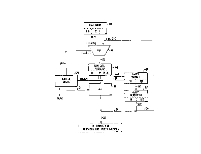
Figure 2 is a block diagram of the preferred embodiment.
As will be described, the present invention improves upon the
performance of the prior art system.
As in the case of the prior art, the invention uses a
parity checker 100 and a parity generator 102 to verify data
passing from a RAM data register 106 to an ALU 110. However, the
parity checker 100 and generator 102 are disposed out of the data
path which couples the RAM data register 106 to the ALU 110,
allowing a direct
~ 2017099
connection via a data path 112. The parity checker 100
tests the data in parallel with the ALU 110 through the
use of parallel data-path 114 and therefore does not
delay the processing of data word 116 by the ALU 110.
5 The ALU 110 normally predicts parity, as described above,
for the result of its operation instead of generating
parity for the result.-: Thus, :the output=of the -ALU 110
will be faulty if faulty data is input. As parity
prediction relies upon the parity of the data word input,
10 if this parity is wrong, erroneous prediction will occur.
Thus, the parity must be generated for the data after a
parity error has occurred.
The original fault tolerant characteristics of
the prior art system need to be preserved. By taking the
15 parity generator 102 out of the direct path between the
RAM data register 106 and the ALU 110, the ALU 110
occasionally- will have a data= word 116 input for which
the parity- 120 is incorrect. If-the-system were allowed
to continue,~downstream destination registers and pari-ty
20 ~he~-ke~s would eventually detect the error and freeze the
system. Thus parity generator 102 is provided to
generate correct parity 122 for the data word 116 as in
the prior art.
The parity checker 100 generates an error signal
25 indicating that a parity error exists for the data word
116. As in the prior art, the error signal is supplied
to a control circuit 124 via path 126 which pauses all
registers and operations which may detect erroneous data
and freeze the machine. The control circuit 124 has
30 other functions in the present invention in addition to
that described above. The control circuit 124 supplies
a signal on path 130 to the ALU 110 to command the ALU
110 to pass the data word 116 appearing at its input
unchanged to its output. As the downstream registers are
35 paused, data appearing on line 132 cannot proceed except
via the alternate path depicted by data paths 134 and
136. On data path 134, there appears only the data word
~ 2~17~99
116 passed by the ALU 110. Generated parity 122, which
is correct for the data word 116 appearing on data path
134, is combined with the data word 116 with both
proceeding along data path 136 to an input of a
multiplexer 140.
The multiplexer 140 is inserted between the RAM
array 142 and the RAM data register 106. A first input
of the multiplexer 140 is connected to the RAM array 142
to provide RAM array data to the RAM data register 106,
and ultimately to the ALU 110. A second input of the
multiplexer 140 is connected to the data path 136 as
described above. An address select signal is supplied
from the control circuit 124 to the multiplexer 140 via
data path 144. It is well known in the art on the use of
a multiplexer to select one of a pair of inputs and
subsequently output data from the multiplexer.
In operation, a data word 116 accessed from the
RAM array 142 is coupled to the first input of
multiplexer 140 via data path 146. In the absence of a
detected error, the multiplexer 140 will have the first
input selected by the control circuit 124, which allows
the data word 116 and its parity data 120 to be passed
to the RAM data register 106 via coupling by data path
150. The data word 116 and the parity data 120 are
temporarily held in the RAM data register 106 until
needed by the ALU 110. When the ALU 110 is ready for the
data, the data word 116 is input into the ALU 110.
During this time, the parity checker 100 begins to test
the parity data 120 against the data word 116 to
determine if a parity error exists. In the usual case,
the parity test will determine that no error exists,
which means that the system has not lost any time as the
ALU 110 has been operating on the data word 116.
In the unlikely circumstance that a parity error
exists, the parity checker 100 will detect the error and
generate an error signal to pass to control circuit 124
via data path 126. It is understood by those of ordinary
' ~ 2017099
skill in the art that an error indication could be as
performed in the preferred embodiment, that is, by
positively generating a signal when an error occurs. It
is also known that an error signal could be the
termination of a signal indicating that parity is good.
The parity generator 102 generates parity for the data
wo,rd 116/passed to it by the parity checker 100 coupled
to the generator 102 via data path 152. The control
circui-t 124 performs three functions upon receiving an
error signal from the parity checker 100. First, the
control circuit 124 issues a signal which pauses all
destination registers downstream from the ALU 110 and
data path 132., This preYents downstream parity checkers
from detecting the parity error and freezing the system.
Second, the control circuit 124 issues a command to the
ALU llO requiring it to pass the data word 116 to its
output, unchanged~ - Thus, the o~riginal data, word 116
appears--at data paths 132 and 134. ,Due to,the fact that
registeEs downstream,from:thç ALU 110 and da,ta-path 132
2Q are_now~;paused, _t~e,-da~,a word- 116 wil,l ~not propagate
downstream:-along data path 132,,-but will only proceed
along data path 134 to data path 136. At data path 136,
the data word 116 (which was passed by the ALU 110), and
the generated parity 122 (which was generated by the
parity generator 102), are combined and,both proceed to
the second input of the multiplexer 140. Third, the
control circuit 124 issues an address select signal to
the multiplexer 140 to command the multiplexer to select
data appearing at its second input, instead of data
appearing at its first input, as is the normal operating
mode without an error indication. The third function of
the control circuit 124 essentially substitutes the
corrected parity data 122 for the original parity data
120 after the corrected parity data 122 has been
associated with the data word 116 for which it had been
generated.
2017099
Thereafter, the data word 116 and the corrected
parity data 122 proceed normally along data path 150 to
the RAM data register 106 where it is temporarily stored.
When the ALU 110 is ready to process the data word 116,
the data word 116 and the corrected parity word 122 are
accessed from the RAM data register 106. The data word
116 is input and processed by the ALU 110, while the
parity checker 100 tests the data word 116 against its
corrected parity data 122. The test will indicate that
the data is good, therefore the control circuit 124 will
now unpause the destination registers downstream from
data path 132, the ALU 110 will be allowed to process the
data word 116, and the multiplexer 140 will once again
select data appearing on data path 146 to output to the
RAM data register 106. The ALU 110 will execute its
instructions upon the data word 116, and the output will
proceed downstream to destination registers and parity
checkers where no parity errors will be detected, and the
system will continue to operate until the error
correction method is complete and purges the data word
116. The data paths of the system remain operating and
unfrozen, the computer continues to operate without
operator intervention. Thus, the desire of improving the
performance of parity checking while preserving the fault
tolerance characteristics of the computing system are
achieved through the use of the novel and ingenious
invention presently disclosed.
While the above provides a full and complete
disclosure of the preferred embodiments of the present
invention, various modifications, alternate constructions
and equivalents will occur to those skilled in the art
given the benefit of this disclosure. For example, the
reference to a RAM data register is only an embodiment.
It would be known to a person of ordinary skill in the
art to substitute any temporary storage device or method,
such as a cache memory, for the register without
departing from the present invention.
'~ 2~l7n~s
Thus,- the invention is not limited to -the
specific embodiment described herein, but is limited as
defined by the appended claims.
.. .. ~
.. . . . . . ..
.. . .
.. _ . . . . . . . .. . . . . . . . . .. ....
.. _ .. ,, ., . . . ... ~ . .. . .
.. .. ... . . . , . ; . . .. .. . . . .
~ . . .. .. , . ~ . ~ .. . . .. . .. ..
:, , - .