Note: Descriptions are shown in the official language in which they were submitted.
2017267
FIELD OF THE lNV~NllON
This invention relates to clipping circuits. More
particulary, it relates to such circuits for clipping
signals substantially symmetrically.
R~CRGROUND OF THE INVENTION
Clipping is the limiting of the amplitude of an
output signal when an input signal is above a given
amplitude. Typically clipping occurs when the amplitude of
the output signal reaches one of the supply rails, or an
output stage driving transistor reaches its maximum output
current by going into saturation or reaching maximum drive
current.
For many applications, especially audio
applications, it is desirable that clipping be performed
symmetrically. Asymmetrical clipping introduces even
harmonics to the output signal. Even harmonics do not
naturally occur in audio signals and their presence can
produce noticeable distortion for a listener.
Where clipping occurs as a result of the output
signal amplitude reaching a supply rail at a different
amplitude, with respect to the normal bias point of the
output stage, from the amplitude at which the driving
transistor reaches its maximum output current asymmetrical
clipping will occur.
2017267
_ - 2 -
As a result, most output stages for applications
where symmetrical clipping is desirable set the output
stage bias point to be midway between one supply rail and
the output voltage when the driving amplifier reaches its
maximum output current. Typically, an output stage will
consist of a bipolar junction transistor (BJT) amplifier
whose emitter is connected to one supply rail and whose
collector is connected through a resistor to the other
supply rail. The input to the output stage is a current at
the base of the transistor, while the output of the output
stage is at the collector of the transistor. The only
factor limiting upward signal excursion, assuming the other
supply rail is a positive supply rail, is the difference
between the bias point at the output and the positive
supply rail. This difference is easily controlled. On the
other hand the factors limiting downward signal excursion
are the current gain of the amplifier, the driving current
at the base of the amplifier and the saturation point of
the amplifier. These factors are processing sensitive and
interdependent. In order to obtain substantially
symmetrical clipping each factor is set up at the time of
processing and cannot be adjusted thereafter. In order to
change the amount of clipping it is necessary to have
separately processed circuits with each of the factors set
for each desired clipping level.
e
3 ~ ~ ~ 7 ~ ~ 7 ~
SUMMARY OF THE INVENTION
The invention provides a clipping circuit, comprising: (a) a
voltage reference stage having generating means for producing a reference
voltage and an output port connected to said generating means for
5 outputting said reference voltage; (b) a transconductance stage having
control means coupled to said output port of said voltage reference stage, a
first current source coupled to said control means, said first current source
including means for generating a drive current having a first pre-
determined value; (c) said transconductance stage further including a gain
10 stage coupled to said first current source for receiving current therefrom,
said gain stage also being coupled to said control means; (d) an input port
for receiving an input signal, said input port being coupled to said output
port of said voltage reference stage and to said control means; (e) said
control means including means responsive to said input signal for
15 controlling the amount of said drive current flowing from said first
current source to said gain stage; (f) said gain stage including means
responsive to the amount of said drive current received thereby for
generating an output current proportional to the amount of said drive
current received by said gain stage and for said output current of said gain
20 stage to have a pre-determined maximum value proportional to said first
pre-determined value; (g) and bias means, including feedback means
connected to said control means, for biasing said control means to control
said gain stage for said output current of said gain stage to have, in the
absence of any input signal, a steady-state value which is substantially one-
25 half of said pre-determined maximum value.
BRIEF DESCRIPIION OF THE DRAWINGS
For a better understanding of the present invention, and to
show more clearly how it may be carried into effect, reference will now be
made, by way of example,
2017257
_ - 4 -
to the accompanying drawings, which show a preferred
embodiment of the present invention, and in which:
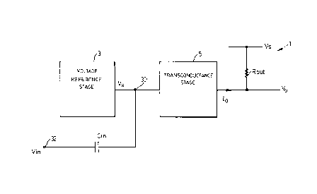
Fig. l is a block diagram of a clipping circuit
according to the preferred embodiment of
the present invention;
Fig. 2 is a circuit diagram of the clipping
circuit of Fig. l;
Fig. 3 is a detailed circuit diagram of the
clipping circuit of Fig. l; and
Fig. 4 is a circuit diagram of the voltage
reference stage with added input
impedance.
DETATT.Rn DESCRIPTION OF THE PREFERRED T~MRODIMFNT
Referring to Fig. 1, the clipping circuit 1 has a
voltage reference stage 3 and a transconductance stage 5.
The voltage reference 3 and transconductance 5 are
connected together and through a coupling capacitor Cjn to
a voltage input Vjn. The output of the transconductance 5 is
connected through a resistor Rout to a first supply rail Vs~
An output voltage, VO~ is between Rout and the output
of the transconductance 5. The transconductance 5 outputs
a current Io as a function of the voltage input Vjn and has
a source of limited drive current ID. The drive current ID
is limited in the sense that it has a given maximum
2017~7
current. The voltage reference 3 outputs a reference
voltage VR.
VR and ID are matched so that a change in VR is
matched by a change in IDmaX such that a bias output current
Iobjas is substantially one-half of a maximum output current
Iomax. The reference voltage VR sets the bias output current
Iobjas for the circuit 1. It will be seen that a change in Vjn
changes the input voltage to the transconductance stage 5,
- which will cause a change in the drive current ID. AS
discussed, to ensure symmetrical clipping the circuit 1
modifies the output bias current Iobias so that it rem~in~
substantially one-half of the maximum output current Iomax.
The output voltage VO is equal to Vs - Rout Io~ During steady-
state operation, the output current Io equals the output
bias current Iobjas, and VObjas is Vs ~ Iobias Rout- The maximum
upward signal swing from VObjas, assuming Vs is positive with
respect to the output of the transconductance 5 and Io is
negative, occurs when Iobjas is zero and is therefore Iobjas
Rout~ The maximum downward signal swing from VObjas is Iomax Rout
~ Iobias Rout- As Imax = 2 Iobjas the maximum downward signal
swing from VObjas is Iobjas Rout~ Thus the upward and downward
signal swings are matched.
Rout acts as a linear current controlled voltage
source.
Referring to Fig. 2, the transconductance 5 may be
implemented using a gain controlled block A between ID and
20~7267
_ - 6 -
VO. The gain block A is driven by ID. The gain of block A
is controlled in that the gain is known and can be
implemented using a substantially processing insensitive
component.
As the gain of block A is controlled the
relationship between the proportion ~f ID and the output
current Io is not affected by processing.
Connected between the source of drive current ID and
the voltage reference is a voltage to current converter 7
outlined in dashed lines. The voltage to current converter
7 determines the amount of drive current ID to be supplied
to the controlled gain block A. The amount of drive current
ID is one-half of the difference between maximum and ~ini~um
drive current when there is a steady-state signaI at the
input to the transconductance. Otherwise, the amount of
drive current ID is proportional to the input to the
transconductance unless the maximum or minimum drive
current is reached.
For the simplest implementation the minimum drive
current should be set to zero (i.e. the source of drive
current is shut off) and the maximum output current Iomax is
twice the steady-state output current Iobjas. When this
happens VO swings between Vs when the drive current is zero
and 2Rout Iobias from Vs- This guarantees symmetrical
clipping.
2017257
- 7 -
In order to communicate when the steady-state has
been reached and what proportion of the maximum drive
current is flowing, the controlled gain block A is
connected back to the voltage to current converter 7. This
connection provides a feedback loop 10.
The voltage reference 3 has a current controlled
first voltage source V1 connected between a first supply
rail, in this case ground GND, and the output of the
voltage reference VR. The first voltage source is controlled
by a second current source Iz.
The voltage to current converter 7 has a current
controlled second voltage source V2 and a voltage controlled
current sink Is~ The current control input of the second
voltage source V2 is connected to the current sink Is and to
the gain block A via the feedback loop 10. The voltage
control of the current sink Is is connected between the
second voltage source V2 and the input to the
transconductance 5. The current sink is connected to the
source of driving current ID.
In operation based on the voltage input Vjnl the
voltage to current converter 7 determines the proportion of
maximum drive current ID presently flowing from the gain
block A and represented in part as the voltage drop across
the second voltage source V2. An increase in the second
voltage source V2 will decrease the voltage at the control
input to the current sink Is~ thereby decreasing the current
- 8 - ~ 7 ~ ~ 7
being sunk. This decreases the output of the voltage to current converter 7
and decreases the amount of drive current ID. Additionally it decreases the
sunk current flowing into the current control input of the second voltage
source V2. Accordingly, when the voltage input Vin reaches a steady-state
value, the transconductance 5 will also reach a steady-state and drive
current ID will also reach a steady-state.
Referring now to Fig. 3, the current controlled first voltage
source V1 has been implemented using a diode connected first BJT Q1 fed
by a third current source I3 and connected through a first passi~ e element
to the second supply raid GND. The first passive element is a resistor Rl.
The second current source I2 is connected to Q1 and R1. The reference
voltage VR is output at port 30, which also constitutes the input port for
the transconductance stage 5. The signal input port for the circuit, for
receiving Vin, is indicated at 32.
The voltage controlled current sink Is is a second BJT Q2
whose base is connected via port 30 to the base of Q1 and to the input
voltage Vin via the capacitor Cin, and whose emitter is connected to the
controlled gain block A implemented by Q4 and Qs as will be later
described.
The current controlled second voltage source V2 is a passive
element, in this case a resistor R2, connected between the emitter of Q2 and
ground.
The source of driving current ID has a first current source I1,
fourth current source I4, and a third BJT Q3. I4 is connected to the collector
of Q2 and the base of Q3. I
,~ '~
2017267
g
is connected to the collector of Q3. The emitter of Q3 iS
connected to ground.
The controlled gain block A has current mirror
connected fourth and fifth BJTs Q4, Q5. The collector of Q4
is connected to I1 and the collector of Q5 iS connected to
the output voltage VO. The emitters of Q4, Q5 are connected
to the emitter ~f Q2.
In operation, the collector current of Q5 iS the
output current Io~ As previously discussed, the condition of
operation for symmetry is Iobjas = ~ Iomax. To show how the
circuit of Fig. 3 achieves this condition it is assumed for
simplicity that the gain block A has a gain of 1. A current
mirror was used to implement the gain block A as the gain
of a current mirror is easily controlled during processing
by fixing the ratio of the physical areas of the BJTs. It
is further assumed that I4 iS approximately equal to I3, Q1
and Q2 having substantially the same gain and R1 has
substantially the same resistance as R2.
I3 will flow through Q1 and I3 and I2 will flow
through R1. This creates the reference voltage at the base
of Q1-
Looking at the transconductance 5, as the gain ofthe current mirror comprising the gain block A is unity,
the current flowing in the collectors of Q4 and Q5 will be
substantially the same. The maximum drive current flowing
20~7267
-- 10 --
into the gain block A will be I1, i.e. when Q3 shuts off.
Therefore Iomax is substantially equal to I1.
It will be seen that by applying an input ~oltage
Vjn, the circuit l is biased and the resultant current
flowing in the feedback loop l0 from the gain block A is 2I1
or 2Iobjas. Symmetrical clipping, i-e- Iobias = 1/2 Iomax~ iS
achieved by making the current source I1 substantially equal
to the current source I2. Applying the well-known
Kirchhoff's Voltage Law around the emitter-base loop of
transistors Q1 and Q2, the following expression is obtained:
-- VR1 -- VBE1 + VBE2 + VR2 ~
Since I3 is substantially the same as I4 and Q1 and Q2 are
matched, the Vbe's ~f Q1 and Q2 will be substantially the
same and drop out of the above expression. Then, VR1 is
equal to VR2, and applying the well-known Ohm s Law, the
following expression is obtained:
(I2 + I3)R1 = (I4 + 2I1)R2
( I2 + I3 )R1 = (I4 + 2Iobias)R2
Since, R1 is substantially the same as R2, and I3 is
substantially the same as I4, the above expression reduces
to 2Iobjas = I2. Therefore, if I1 is substantially equal to I2,
then Iobjas is equal to 1/2 I1 or 1/2 IDmax-
Should Iobjas not substantially equal twice I2 thenthe voltage across R2 will be too high or too low. Should it
be too low Q2 will turn on harder, drawing current away from
the base of Q3 . Less current will flow from I1 into Q3 and
2 ~ 7
more into the gain block A. More current will flow out of the gain block A
into R2 to raise the voltage across R2 until Iobias reaches 1/2 I2. The
opposite effect will occur when the voltage across R2 is too high. Thus if I
is substantially the same as I2 then Iobias will be one-half of Iomax
The gain of Q3 must be sufficiently high to not dra~ away
significant current from Q2 affecting the mirroring process. Q3 acts as a
current controlled current sink sinking current away from Il. It will be
seen that Q2 and Q3 act together as a steering circuit, controlling how
current I1 is divided between current sink Q3, and gain stage A. It will also
be seen that Q4 and Q5 are a current-controlled current amplifier with
predictable gain, i.e. Q4 receives a controlled current (all or part of Il) and
Q4, Q5 each output a current which is proportional to the current received
by Q4.
It is possible to make devices where Iobias is substantially one-
half of Iomax without having I1 and I2, 13 and I4, R1 and R2, Ql and Q2, and
Q4 and Q5 substantially the same. It is important though to match these
components to ensure the ultimate circuit 1 does meet the Iobias is
substantially one-half Iomax criterion.
For example, where Q5 has twice the gain of Q4 the gain of the
gain block A will be approximately 2. IomaX will be twice Il. As discussed, to
achieve symmetrical clipping Iobias must be 1/2 Iomax and therefore Iobias
must be equal to Il. In these circumstances I2 should equal one-half the
gain of the gain block A plus one-half, multiplied by Il.
Other matching of the components will be evident to those
skilled in the art.
~. ~.
. ~
2017267
- 12 -
Another advantage of the circuit l is that the
small signal voltage gain is independent of the clipping
level. For a change in Vjnr the Vbe ~f Q2 will lag behind the
change causing the voltage across R2 to change. The change
in the voltage across R2 will draw a proportionally
different current through the gain block A into R2. This
changes Io by one-half the change in the current in the gain
block A. VO will change by a factor of Rout times the change
in Io~ Thus the small signal gain of the circuit is
approximately
Rout
R2 tl + ~)
where ~ is the gain of the gain block A.
Referring now to Fig. 4, resistor R3 between the
base and collector ~f Q1, and resistor R4 between the
collector of Q1 and the connection of the coupling capacitor
Cin and the base ~f Q2, may be added to increase the input
impedance seen by Vjn. R3 and R4 should be matched, and for
simplest implementation be substantially the same, to keep
the mirroring effect ~f Q1 and Q2.
Other embodiments of the present invention will be
evident to those skilled in the art and fall within its
spirit and scope, as defined by the following claims.