Note: Descriptions are shown in the official language in which they were submitted.
~ 2 0 1 7 5 ~ ~
CODED I~PLNSMISSION SYSTEM WITE~ T~ITrAT.T7.TNG COD~
BACKGRO~ND OF TXE lNV~'\lllON-
(1~ Field of the Invention
The present invention relates to a coded
transm.ission system wherein each bit of transm.itted data
having a logical value is coded depending on a coded
result of a preceding bit The present invention urther
relates to a line coding apparatus and a line decoding
apparatus used in the above coded trAn~ ; on system
Line coding systems wherein each bit of data
having a logical value is coded 9l~r~n~1;ns on a coded
result of a preceding bit, e 9, the bipolar coding
system, or the CMI (coded mark inversion) coding
system, are used for line coding of trAn~ n of a
logical value
In the bipolar coding system, each bit of data
having a logical value ,,0u is coded to a zero level, and
each bit of the data having a logical value U1U is
alternatively coded to a posïtive level and a negative
level, i e , each bit of the data having a logical value
~1u is coded to the positive level when a preceding bit
of the da~a having the logi~l value UlN ~is coded to the
negatlve level, and each bit of the data having a
logical value UlN is coded to the negative level when a
preceding bit of the data having the logical value "lN
is coded to the positive level In the C~I coding
system, each bit of data having a logical value UON is
coded by changing the coded signal level fFom a zero
( UON ) level to a positive ( UlN ) level in the center
phase of one cycle, and each bit of the data having a ~
logical value NlN is alternatively coded to the positive
(UlN) level and the zero (UON) level, i e, each bit of
the data having a logical value UlN is coded to the
positive ( UlN ) level when a preceding bit of the data
having the logical value UlN is coded to the zero ( UON )
level, and each bit of the data having a logical vaLue
~r
2 20 1 7555 FJ 7909 CA
is coded to the zero ( ~0" ) level when a preceding
bit of the data having the logical value ~ is coded to
the positive ("1~) level. In both coding systems, a code
which does not accord with the above rules, is
5 determinea to be a violation of the rules, respectively,
in the receiver side. ~amely, in the above coding
systems, a line decoder in the receiver side is required
to memori2e a coded mar]~ (level) of a preceding bit of
data having a logical value "1".
In the recent data tr;~n~m; qq;on systems, high
speed tr~n~; qq; on is required In particular, in data
processing systems wherein a plurality of data
processing apparatuses are connected with each other by
data tr~n~ c;on lines, data is transmitted
15 asynchronously between the apparatuses In such
asynchronous data transmission systems, use of the CMI
coding is considered to be advantageous because the CMI
coded signal can be relatively easily synchronized in
the receiver side.
(2) Description of the Related Art
In the above asynchronous transmission systems
wherein a plurality of data processing apparatuses are
connected with each other by data transmission lines, a
25 receiver in each of the data processing apparatuses or
data transmission apparatuses receives coded signals
which are transmitted from a plurality of data
processing apparatuses or data tri~n~ ~; qq; t-n apparatuses .
When the above line coding systems wherein each bit of
30 data is coded depending on a coded result of a preceding
bit, like the bipolar coding system, or the CMI coding
system, are used for line coding in the above data
transmission system, each receiver is required to
memorize a coded mark (level) of a preceding bit of data
35 having a logical value 'V1" for each of a plurality of
data processing apparatuses or data transmission
apparatuses from which coded signals are asynchronously
20t755~ -
J~ 3 - FJ-7909-Q
transm. itted to the receiver . However, such memorizing i8
very bothersome, or almost impossible.
In addition, in the above asynchronous data
transmission system.s, a synchronization pattern is
transm. itted preceding a real message portion . Figure 1
shows an example of a h~ginn;n~ portion of a
conventional asy-nchronous tr~n~ 2R;on signal using the
CMI coding. In the exam~ple of Fig. 1, a ~y~ Lullization
pattern which is comprised of three synchronization bits
"000" is transmitted preceding a real message portion,
i.e, the CMI-coded level (010101) is transmitted pre-
ceding a CMI-coded real message portion. However, each
bit of the synchronization pattern may be recognized er-
roneously because the receiver is generally not
synchronized with the asynchronous transmission signal
when receiving the synchronization pattern. Figure 2
shows an example of an erroneously re~n~n;7ed beginning
portion of a conventional asynchronous transmission
signal using the CMI coding In the example of Fig. 2,
the code (01) of the second bit of the synchronization
pattern is erroneously recognized as (11), i e, the
second bit of the synchronization pattern is erroneously
rf~ogn~7~1 as "lD. R~pr~n-9;n~ to the recognition of the
(11), the receiver memorizes the reception of the code
(11), and when a bit of the real message having a
logical value ~ v is trans~m~itted to the receiver with
coded as (11) following the eLlUll~UU:~ recognition, the
receiver determines the received code (11) as a
violation of the rule of the CMI coding.
Namely, in the above asynchronous data
tr~n~ nion systems wherein each bit of data is coded
d~p~n-q;n~ on a coded result of a preceding bit, as the
above CMI coding, the coded signal may not be correctly
decoded in the receiver side.
2 [ ~ 75~5
S~JMMARY OF THE I~IVENTION
A feature of one embodiment of the present invention is to
provide a coded transmission system wherein each transmitted
message can be correctly recognized in a receiver without being
5 affected by a coded signal of a message which has been previously
received at the receiver, or by an erroneous recognition of a bit
of a synchronization pattern.
Another feature of an embodiment of the present invention
is to provide a line coding apparatus and a line decoding
10 apparatus used in the above coded transmission system.
In accordance with an ~mh,ml; r -nt of the present invention
there is provided a coded transmission system for transmitting
data including a resetting bit and a message, wherein each bit
of transmitted data, having a logical value, is coded dpp~n~1in~
15 on a coded result of a bit most recently transmitted before each
bit, the coded transmission system comprising: sending-side
apparatus including at least first preceding code memorizing
means for memorizing a first stored code representing a code of
a bit last transmitted to code a bit to be transmitted next, and
20 for resetting the first stored code to an initial code which
indicates a start of a message in response to the resetting bit;
coding means for receiving the resetting bit and the message, for
coding each bit of the message in accordance with a prede~rm;n-
~coding rule and the first stored code to produce a coded result,
25 and for coding the resetting bit to a predetermined resetting
code, the predetermined resetting code is different from the
codes used in the coding of the message; and transmitting means
for transmitting the predetermined resetting code and for trans-
mitting the coded result of the message after the transmission
30 of the resetting code; receiver-side apparatus including at least
second preceding code memorizing means for memorizing a second
stored code representing a code of a bit last received to decode
a code of a bit received next; receiving means for receiving the
predetermined resetting code, and the coded result of the mess-
A
.. . . . .. . ..
201 7555
-- 5 --age; resetting means for resetting the second stored code to the
initial code in response to the predetermined resetting code; and
decoding means for decoding the coded result received correspon-
5 ding to the message in accordance with the predetermined codingrule and the code memorized by said second preceding code
memorizing means; and transmission line means for connecting the
sender-side apparatus with said receiver-side apparatus.
In accordance with another ~ ; r -nt of the present
10 invention there is provided an apparatus provided in a sender
side of a coded transmission system for transmitting data
including a resetting bit and a message, wherein each bit of
transmitted data, having a logical value, is coded ~l~rPn~lin~ on
a coded result of a bit, most recently transmitted before each
15 bit, the apparatus comprising: preceding code memorizing means
for memorizing a stored code representing a code of a bit last
transmitted to code a bit to be transmitted next, and for
resetting the stored code to an initial code which indicates a
start of a message in response to the resetting bit; coding means
20 for receiving the resetting bit and the message, for coding each
bit of the message in accordance with a predet~rr;n,~cl coding rule
and the stored code to produce a coded result, and for coding the
resetting bit to a resetting code, the resetting code is differ-
ent from the codes used for the coding of the message; and
25 transmitting means for transmitting the resetting code, and for
transmitting the coded result of the message after transmission
of the resetting code.
In accordance with a further embodiment of the present
invention there is provided a sender-side apparatus provided in
30 a sender side of a coded transmission system for transmitting
data including a synchronization pattern, a resetting bit and a
message, wherein each bit of transmitted data, having a logical
value, is coded depending on a coded result of a bit most
recently transmitted before each bit, the apparatus comprising:
35 preceding code memorizing means for memorizing a stored code
~ " .,A
_ _ _ _ _ _ _ . , . ,, _ _ . . .
20 ~ 7555
-- 6 --
representing a code of a bit last transmitted to code a bit to
be transmitted next, and for resetting the stored code to an
initial code which indicates a start of a message in response to
5 the resetting bit; coding means for receiving the synchronization
pattern, the resetting bit, and the message, for coding each bit
of the synchronization pattern and the message in accordance with
a predetermined coding rule and the stored code to respectively
produce a synchronized code and a coded result, and for coding
10 the resetting bit to a re6etting code, the resetting code is
different from the codes used for the coding of the synchroniza-
tion pattern and the message; and transmitting means for trans-
mitting the synchronized code of the synchronization pattern, for
transmitting the resetting code after the transmission of the
15 synchronized code, and for transmitting the coded result of the
message after transmission of the resetting code.
In accordance with yet another embodiment of the present
invention there is provided a method for transmitting coded data,
the method comprising the steps of: (a) receiving a message to
20 be transmitted; (b) generating a resetting bit; (c) rese1:ting a
last transmitted code to an initial code which indicates a start
of a message based on the resetting bit; (d) coding the resetting
bit into a resetting code; (e) coding the message into a coded
message in accordance with a prP~et~rm;n~d coding rule and the
25 last transmitted code; (f) transmitting the resetting code
followed by the coded message; and (g) storing the last trans-
mitted code.
In accordance with a further embodiment of the present
invention there is provided a line coding apparatus provided in
30 a sender side of a coded transmission system, the coded trans-
mission system transmits data, the data transmitted corresponds
to a resetting bit and a me5sage, comprising: preceding code
memorizing means for memorizing a stored code representing a code
of a bit last transmitted to a code a bit to be transmitted next,
35 and for resetting the stored code to an initial code in response
. ~
_ _ _ _ , . . _ .. .. . . . _ _ _ _
20 1 75~
-- 7 --
to the resetting bit; and coding means for receiving the reset-
ting bit and the message to be transmitted after the resetting
bit, for coding each bit of the message in accordance with a
predetP~n;n~d coding rule and the stored code, and for coding the
resetting bit to a predet~rm;n~ resetting code, the predeter-
mined resetting code is different from the codes used for the
coding of the message.
In accordance with a still further Pmh~ nt of the present
invention there is provided a line /~F.ro~l i n~ apparatus provided
in a receiver side of a coded tri~ncmificion system for receiving
coded data, the coded data includes a coded result and a reset-
ting code, comprising: preceding code memorizing means for
memorizing a stored code representing a code of a bit last
received to decode a code of a bit received next; resetting means
for resetting the stored code to a predetermined initial code in
response to the resetting code; and decoding means for decoding
the coded result received corresponding to the message in accor-
dance with a predet~rm;nP~ coding rule and the stored code.
BRIEF DESCRIPTION OF T~E DRAWINGS
In the drawings:
Figurè 1 shows an example of a beginning portion of a
conventional asynchronous transmission signal using the CMI
2 5 coding;
Figure 2 shows an example of an erroneously recognized
beginning portion of a conventional asynchronous transmission
signal using the C~I coding;
Figure 3 shows an example of the insertion of the initia-
lizing (resetting~ bit according to the present invention;
Figure 4 shows an embodiment of the line coder according to
the present invention;
Figure 5 shows the input-output relationship in the memory
3 in Fig. 4;
Figure 6 shows an example of the operation of the construc-
. ._
. . ~
20 1 7555
-- 8 --
tion of Fig. ~;
Figure 7 shows an embodiment of the line decoder according
to the present invention;
Figure 8 shows the input-output relationship in the memory
14 in Fig. 7; and
Figure S shows an example of the operation of the construc-
tion of Fig. 7.
DESCRIPTION OF THE t'~klW~'L) EMBODIMENTS
(1~ Basic Operations of First and Second Aspects of the
Present Invention.
Before describing the preferred embodiment of the present
invention, first, the basic operations of the various aspects of
the present invention are o rrl ~ i no~1 below.
According to the first aspect of the present invention, in
the sender-side apparatus, f irst, a resetting bit is generated
in the resetting bit generating circuit, and next, a message is
generated in the message generating circuit . Ro~r-~n~ i n~ to the
generated resetting bit, the content of the first preceding code
memorizing circuit is reset to an initial code, where the first
preceding code memorizing circuit memorizes a code of a bit which
is lafit transmitted from the sender-side apparatus. The reset-
ting bit is coded to a resetting code, and the resetting code is
transmitted to the receiver-side apparatus through the tr~nC.n;~-
sion line. Next, each bit of the message is coded in a predeter-
mined rule and the content of the first preceding code memorizing
circuit, where the predetorm;n~(1 rule determines the manner of
the coding wherein each bit of transmitted data having a logical
value i5 coded depending on a coded result of a preceding bit.
In the receiver-side apparatus, first, the above resetting code
is received. Responding to the reception of the resetting code,
the content of the second preceding code memorizing circuit is
reset to an initial code. Following the resetting code, each bit
of the message is received, and is decoded in the decoding
_, _ . . _ _ . .. . _ _ _ .
-- 2017555
L
- 8a -
circuit in accordance with the above pre~lot~rminPd rule and the
content of the second preceding code memorizing circuit. Since
both the contents of the first preceding code memorizing circuit
5 in the sender-side apparatus and the second preceding code
memorizing circuit in the receiver-side apparatus are reset to
an initial code ~efore codlng a message and before decoding the
coded signal of the message for each transmission of a message,
coding of each message and decoding O e the coded signal of the
10 message are begun from the same initial condition using the same
initial code. Therefore, even when the receiver-side apparatus
;nrl~rr~nAr~ntly receives coded signals of messages from a plurality
of sender-side apparatuses, a coded signal of each message can
be correctly decoded in the receiver-side apparatus without being
15 affected by a coded signal of a message which has been previously
received .
According to the second aspect of the present invention, in
the sender-side apparatus, first, a synchronization pattern is
generated in the synchronization pattern generating circuit,
20 secondly, a resetting bit is generated in the resetting bit
generating circuit, and then, a message is generated in the
message generating circuit. The synchronization pattern is coded
in accordance with a predet~rm;ne~1 rule, and the coded signal is
transmitted to the receiver-side apparatus through the transmis-
25 sion line. Next, r~sp~n~;n~J to the generated resetting bit, thecontent of the first preceding code memorizing circuit is reset
to an initial code, where the first preceding code memorizing
circuit memorizes a code of a bit which is last transmitted from
the sender-side apparatus. The resetting bit is coded to a
3 0 r~setting code, and the resetting code is transmitted to the
20 t 75~5
- 9 - FJ-7909-CA
receiver-side apparatus through the tr~nr~;ssi-~n line.
Then, each bit of the message is coded in a
pr~l~t~rm;n~ rule and the content of the first
preceding code memorizing circuit, where the
5 predetermined rule d~t~ ;n~ the manner of the coding
wherein each bit of transmitted data having a logical
value i5 codea ~l~r~n~l;n~ on a coaea result of a
preceding bit. In the receiver-side apparatus, first,
the above coded signal of the synchronization pattern is
10 receivea, ana the timing of reception of signals is
adjusted in a~,Ld~ e with the received synchronization
pattern Next, the resetting code is received
Responding to the reception of the resetting code, the
content of the second preceding code memorizing circuit
15 is reset to an initial code. Following the rl~cett i n~
code, each bit of the message is received, and is
decoded in the ~le<~ ;n~ circuit in accordance with the
above preaetermined rule and the content of the second
preceaing coae memorizing circuit. Since both the
20 contents of the first preceding code memorizing circuit
in the sender - side apparatus and the second preceding
code memorizing circuit in the receiver-side apparatus
are reset to an initial code before coding a message and
before decoding the coded signal of the message for each
25 transmission of a message, similar to the above first
aspect of the present invention, coding of each message
and decoding of the coded signal of the message are
begun f rom the same initial condition using the same
initial code. Therefore, even when the receiver-3ide
30 apparatus independently receives coded signals of
- gc_ from a plurality of sender-side apparatuses, a
coded signal of each message can be correctly decoded in
the receiver-side apparatus without being affected by a
coded signal of a message which has been previously
35 receivea. In addition, since the resetting code is
transmitted after the synchronization pattern and before
the coded signals of the message, the decoding of the
..... . _ . . .
~ 20 1 7555
- 10 - FJ-7909-CA
message can be correctly carried out without being
affected by an erroneous recognition of a bit of a
synchronization pattern.
(2) Details of the Preferred r ~
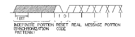
Figure 3 shows an example of the insertion of the
init;~li7;ng (resetting) bit according to the present
invention in the case the CMT coding is used. Since the
code mark (10) is not used in the normal CMI coding
rule, the code mark (10~ is defined as the resetting
code in the ~1; t of the present invention, and is
inserted between the synchronization pattern and a real
message portion in each asynchronous transmission bit
sequence .
Figure 4 shows an embodiment of the line coder
according to the present invention. The line coder of
Fig. 4 is provided in the sender-side apparatus for
coding bit seguence which includes a synchronization
pattern, a resetting bit, and a real message portion
which ~ nt~;n~: an indication of an address, an
indication of a sender, and information which is to be
transmitted to the receiver side In Fig . 4, ref erence
numerals 1, 2, and 5 each denote a flip-flop circuit, 3
denotes a memory circuit, 4 denotes a selector, and DL
denotes a resetting bit, and CMI denotes a coded signal
on the transmission line
The flip-flop circuit 1 serially receives each bit
of the synchroni2ation pattern and the message at its
data input terminal. The input signal of the flip-flop
circuit 1 is denoted by DATA. The synchronization
pattern is generated in a pattern generator in a
communication control circuit which is not shown but
generation of a synchronization pattern is well known in
the conventional com~ nication technigue, and the
message are generated in a data processing portion in
the sender-side apparatus which is not shown because the
generation of the message is not the characteristic
.. , . . ... . .. _ . _ _ _ _ . _ . _ . . . .. . . _
~ 20 1 7555
feature of the present invention. The resetting bit DL is
generated in the above communication control circuit. The
resetting bit DL is made active "1" by the communication control
5 circuit after the generation of the synchronization pattern, and
is supplied to a data input t~m;n~l of the flip-flop circuit 2
after all bits of the synchronization pattern have been supplied
to the flip-flop circuit 1 from the data, and in the other
instances, the resetting bit DL is inactive "0". The above
lO inputs of the flip-flop circuits l and 2 are latched in the flip-
flop circuits l and 2, respectively, and the outputs of the flip-
flop circuits 1 and 2 are respectively applied to the input ter-
minals Al and A2 of the memory circuit 3. The output of the
flip-flop circuit 5 is applied to the other input t~l~m;n:~l Sl of
15 the memory circuit 3. The memory circuit 3 outputs Bl, B2, and
S2 signals responding to the above inputs Al, A2, and Sl, and the
input-output relationship of the memory 3 is shown in Figure 5.
The output S2 is applied to the data input t~ m;ni31 of the flip-
flop circuit 5, and is latched in the flip-flop circuit 5. All
20 the flip-flop circuits 1, 2 and 5 operates synchronized with a
clock signal CLK which synchronizes with each bit of the synchro-
nization pattern and the message. The outputs Bl and B2 are
applied to the selector 4, and the selector 4 selects one of its
inputs Bl and B2 as its output. The selector 4 receives the
25 above clock signal CLK as its selection control signal. The duty
ratio (mark ratio) of the clock is 50%, and therefore, the
selector 4 selects the signal B1 in a half cycle of the clock
CLK, and selects the signal B2 in the other half cycle of the
clock CLK for each bit. The output of the selector ~ is the
30 above-mentioned coded output CNI of the line coder of Fig. 4.
When the resetting bit DL is "0" and a bit of data which is
applied to the flip-flop circuit 1 is "0", i.e., correspondingly,
both the inputs Al and A2 are
r
201 7555
- 12 - FJ-7909-CA
"O~, the output B1 i8 "O" and the output B2 is ~
regardless of the input S1, and the output S2 is the
same as the input S1 at the instance. Namely, the
content of the flip-flop circuit 5 i5 u~lvll~lged when
5 both the inputs A1 and A2 are ~0~ Thus, the CMI-coded
output from the selector 4 corrP~:r~-n~l;n~ to a data bit
"O" is (01)
When the resetting bit DL is "0" and a bit of data
which is applied to the ~lip-flop circuit 1 is ~
10 i.e., correspondingly, the input A1 is "1 and the input
A2 is ~0~, the outputs (B1, B2~ are (1, 1) and (0, 0)
depending on whether the input S1 at the instance is "0"
or "l'V, respectively. When a bit of data which is
applied to the flip-flop circuit 1 is A'1", the content
15 of the flip-flop circuit 5 is changed ~rom "1" to ~0",
or from ~on to ~'1", the changed output S2 is latched in
the flip-flop circuit 5, and is applied to the input
terminal S1 of the memory circuit 3 in the next cycle.
Thus, the CMI-coded output from the selector 4
20 corresponding to a data bit "0" alternatively becomes
(11) and (00).
When the resetting bit DL is "1", and
co.L~:,yv~ ingly the input A2 becomes "1~', the outputs
(B1, B2) are (1, 0) regardless of the input A1 of the
25 memory circuit 3, and the output S2 becomes ~0". Thus,
the rPcettin~ code (10) is output from the selector 4,
and the output of the flip-flop circuit 5 is reset to
~O~V,
Figure 6 shows an example of the operation of the
30 construction of Fig. 4. At the time tO, the resetting
bit DL becomes ~1". At the time tl, the clock signal CLR
rises, the "1" state of the resetting bit DL is latched
in the flip-flop circuit 2, and the output of the flip-
flop circuit 2 is applied to the memory circuit 3 as the
35 input A2. RP~lronrl;n~ to the "1" state of the input A2,
the output CMI of the selector g becomes "1", and then,
the output CMI of the selector 4 becomes "0" responding
~ _ , , . , . , . , . _ . .. . . _ .... _ ~ .. . . .. .. . .
J 20 1 7555
-- 13 --
to the fall of the clock signal CLK at the time t2. When the
resetting bit DL returns to "0", the output of the flip-flop
circuit 2 i6 reset to "0" at the time t3, and thereafter, the
selector 4 outputs a CMI-coded signal responding to each input
bit DATA of the flip-flop circuit 1.
Figure 7 shows an embodiment of the line decoder according
to the present invention. The line decoder of Fig. 7 is provided
in the receiver-side apparatus for decoding coded signals corres-
ponding to the above-mentioned bit se~uence which includes a
synchronization pattern, a resetting bit, and a real message
portion which contains an indication of an address, an indication
of a senaer, and information which is to be transmitted to the
receiver side. In Fig. 7, reference numeral 11 denotes a
selector, 12, 13, 15, 16, 17, and 18 each denote a flip-flop
circuit, 14 denotes a memory circuit, and DL' denotes a decoded
resetting bit, CMI denotes the above-mentioned coded signal on
the transmission line, CLK denotes a receiving clock, DATA
denotes a decoded bit, and V denotes a violation bit.
The selector 11 serially receives the above coded signal at
its data input t~rminAl . The sector 11 has two output torm;n ~1 s,
and receives the receiving clock CLK at its control input ter-
minal. The receiving clock CLK is extracted from the received
coded signal, and the duty ratio of the clock signal is 50%.
Thus, the selector 11 delivers its input to one of its two output
t~rmin~lR~ alternatively, for every half cycle of the receiving
clock CLK. Since the CMI-coded signals are defined by their
signal levels in every half cycle as explained before, a signal
level of the CMI-coded signal in the first half of each cycle of
the receiving clock CLK is delivered to the flip-flop circuit 12
and a signal level of the CMI-coded signal in the second half of
each cycle of the receiving clock CLK is delivered to the flip-
flop circuit 13. These delivered signal levels are respectively
latched in the flip-flop circuits 12 and 13 at each rising time
of the receiving clock CLK. All the flip-flop circuits 12, 13,
,
_. ~
201 7555
15, 16 and 17 operate synchronized with the receiving clock
signal CLR. The outputs of the flip-flop circuits 12 and 13 are
respectively applied to the input ~Prm;nAl~ C1 and C2 of the
5 memory circuit 14. The output of the flip-flop circuit 17 is
applied to the other input t~rm;nAl S3 of the memory circuit 14.
The memory circuit 14 outputs Dl, D2, S4, and S5 signals respon-
ding to the above inputs C1, C2, and S3, and the input-output
relationship of the memory 14 is shown in Figure 8. The output
10 S4 is applied to the data input t~ n;nAl of the flip-flop circuit
17, and is latched in the flip-flop circuit 17. The output
signals D1 and D2 of the memory circuit 14 are respectively
applied to the flip-flop circuits 15 and 16, and are respectively
latched in the flip-flop circuits 15 and 16. The flip-flop
15 circuit 15 serially outputs decoded bit sequence DATA, and the
flip-flop circuit 16 outputs a decoded resetting bit DL'. The
output S5 of the memory circuit 14 is latched in the flip-flop
circuit 18, and is then output as a violation bit V. The above
decoded results DATA and DL', and V are supplied to a data
20 processing portion in the receiver-side apparatus which is not
shown .
When the received CMI code is (01), and COLL- ~r~ ;nqly, the
inputs C1 and C2 are (0, l), the output Dl of the memory circuit
14 is "0", and the output S4 is the same as the input S3 at the
25 instance. Namely, when the received CNI code is (01), the con-
tent of the flip-flop circuit 17 is unchanged. In addition, the
output D2 is "0". Thus, the decoded bit "0" of the received CMI
code (01) is obtained through the flip-flop circuit 15, and the
decoded result DL' of the resetting code, which is obtained
30 through the flip-flop circuit l~, is "0".
2017555 , 1~
- FJ-7909-CA
When the received C~ code is (11), and
correspondingly, the inputs C1 and C2 are ( 1, 1 ), ~ e
output D1 of the memory circuit 14 is ~lN, and the
output S4 is ~ln In addition, the output D2 is NON
5 Thus, the decoded ~it NlN Of the received C~I code ~11)
is obtained throug~ the flip-flop circuit 15, and the
decoded result DL' of the resetting code, which is
obtained through the flip-flop circuit 16, is NON.
Similar to the above, when the received CMI code
10 is (00), and correspondingly, the inputs C1 and C2 are
(0, 0), the output D1 of the memory circuit 14 is NlN,
and the output S4 is UON~ In addition, the output D2 is
'ON Thus, the decoded bit ~lN of the received CMI code
(00) is obtained through the flip-flop circuit 15, and
15 the decoded result DL' of the resetting code, which is
obtained through the flip-flop circuit 1~, is NON.
When the received CMI code is (10), and
correspondingly, the inputs C1 and C2 are (1, 0), tlle
output D2 is NlN In addition, the outputs D1 and S4 of
20 the memory circuit 14 are NON Thus, the decoded
resetting bit NlN of the resetting code (10) is obtained
as the output DL' the flip-~lop circuit 16, and the
decoded bit DATA o the received code, which is obtained
through the flip-flop circuit 15, is "ON.The contert S3
25 of the flip-flop circuit 17 is reset to ~ON r~cp-~n~9;ng
to the reception of the above output S4, corresponding
to that the above line coder of Fig_ 4 is constructed so
that the first bit having a logical value ~lN in each
bit sequence following a resetting bit, is coded to
30 (11). Further, The above-mentioned data processing
portion in the receiver- side apparatus ignores the bit~
DATA, and r~ gn; 7.0C the beginning o the real message
portion in a bit sequence when the resetting ~it DL' is
When the CMI code (00) is repeatedly received,
i.e., all of the inputs C1, C2, and S3 are NON, the
output S5 of the memory circuit 14 becomes N1N, and thus
f-- ~
20 1 7555
- 16 - FJ-?909-CA
the violation bit V becomes "1~. S~r~ilarly, ,vhen the CMI
code (11) is repeatedly received, i e, all of the
inputs Cl, C2, and S3 are Dl'', the output 55 of the
memor~ circuit la~ becomes "1~', and thus the violation
5 bit V becomes ~1".
Figure 9 shows an example of the operation of the
constructiorL of Fig 7. At the time t6, the resettil~g
code (10) is received, ~1~' is latched in the flip-flop
circuit 12 and '0~ is latched in the flip-flop circuit
10 13, i . e., the inputs Cl and C2 respectively become "l~r
ana ~'0~ at the next rising time t7 of the receiving
clock . Responding to the above inputs Cl and C2 ( 1 , O ~,
the decoded resetting bit DL' becomes "1", and the
output S3 of the flip-flop circuit 17 is reset to ~0~ at
15 the next rising time t8 of the receiving clock. In
parallel to the above operation, at the time t7, the C~I
code (01) is received, ~0" is latched in the flip-flop
circuit 12 and ~ ' is latched in the flip-flop circuit
13, i . e., the inputs Cl and C2 respectively become i'O"
20 and ~'1" at the next rising time t8 of the receiving
clock. Responding to the above inputs Cl and C2 (O , 1~,
the decoded bit DATA becomes "O~', the output DL' of the
flip-flop circuit 16 becomes ~ON, and the output 53 of
the flip-flop circuit 17 is unchanged at tbe next rising
25 time t9 of the receiving clock. Further, in parallel
with the above operation, at the time t8, the C'qI code
(11) is received, ~ is latched in the flip-flop
circuit 12 and "1" is latched in the flip-flop circuit
13, i . e ., the inputs Cl and C2 respectively become Ul''
3 0 and "1~ at the next rising time tg of the receiving
clock . Responding to the above inputs Cl and C2 ( 1 , 1 ),
the decoded bit DATA becomes ~ , the output DL~ of the
flip-flop circuit 16 is "O", and the output s3 o the
flip-flop circuit 17 is changed to "1" at the next
35 rising time tlO of the receiving clock. Next, in
parallel with the above operation, at the time t9, the
CMI code ~01) is received, "O" is latched in the flip-
._ ,
..~=
~ 20 1 7555
-- 17 --flop circuit 12 and "1" is latched in the flip-flop circuit 13,
i.e., the inputs Cl and C2 respectively become "O" and "1" at the
next rising time tlO of the receiving clock. RP~rnn~l~ng to the
5 above inputs Cl and C2 (O, 1), the decoded bit DATA becomes ~'0~',
and the output DL' of the flip-flop circuit 16 iB 1~Oll, and the
output S3 of the flip-flop circuit 17 is lln~h~n~Pd at the next
rising time tll of the receiving clock. Further, in parallel
with the above operation, at the time tlO, the CMI code (00) is
10 received, "O" is latched in the flip-flop circuit 12 and "O" is
latched in the flip-flop circuit 13, i.e., the inputs Cl and C2
respectively become "O" and "O" at the next rising time tll of
the receiving clock. ~Pclr~m~l; n~ to the above inputs Cl and C2
(O, O), the decoded bit DATA becomes "1", the output DL' of the
15 flip-flop circuit 16 is "O", and the output S3 of the flip-flop
circuit 17 is changed to "O" at the next rising time tl2 of the
receiving clock.
The many features and advantages of the invention are
apparent from the detailed specification and thus it is ~ntPn~lPd
20 by the ArpPn-7Pd claims to cover all such features and advantages
of the invention which fall within the true spirit and scope
thereof. Further, since numerous modifications and changes will
readily occur to those skilled in the art, it is not desired to
limit the invention to the exact c:u,l_l L~l.ion and operation
25 illustrated and described, and ~ccordingly all suitable modi-
fications and equivalents may be resorted to as falling within
the scope of the invention.
.
. ~,