Note: Descriptions are shown in the official language in which they were submitted.
PHN 12.970 1 24.04.1990
Integrated memory comprising a sense amplifier.
The invention relates to an integrated field-effect
transistor memory comprising memory cells which are arranged in rows and
columns, each column of memory cells being connected to a bit line and a
non-bit line by way of selection means, and also comprising at least one
sense amplifier which comprises a first and a second input for coupling
to a bit line and an associated non-bit line of a column, each of which
is coupled to a supply terminal via a load, which sense amplifier
performs a current measurement on the first and the second input during
the reading of information on the first and the second input, and which
sense amplifier comprises a parallel connection of a first and a second
current branch, each current branch comprising a control transistor
having a gate, a source and a drain, the source of the control
transistor in the first and the second current branch being connected to
the first and the second input, respectively. A memory of this kind is
known from the article "Design tricks speed up INMOS~s SRAMS" in
"Electronics", April 16, 1987, p. 34. The cited article describes a
memory in which a sense amplifier senses and amplifies the information
on bit lines by detection of current instead of the detection of voltage
differences. Consequently, the processing speed of such a sense
amplifier is substantially independent of the parasitic b.it line
capacitance, so that a memory design may be simpler.
It i.s inter olio an abject of the invention to
provide an implementation of such an integrated memory in which also the
susceptibility to interference is less.
To achieve this, an integrated field-effect transistor
memory in accordance with the invention is characterized in that the
sense amplifier also equalizes the voltages on the first and the second
input during the current measurement, the gate of the control transistor
in each current branch being connected to the drain of the control
transistor in the other current branch, the channel of a load
transistor, comprising a gate, a source and a drain, being connected
between the drain of the relevant control transistor and a supply
PHN 12.970 2 24.04.1990
terminal in each current branch, said load transistor being of the same
conductivity type as the control transistor in the relevant current
branch, the coupled gates of said load transistors receiving a selection
signal for the selective activation of the sense amplifier. An
integrated memory .in accordance with the invention offers the advantage
that the sense amplifier is constructed using only 4 transistors, the 4
transistors providing full equalization of the voltages on the inputs of
the sense amplifier.
An embodiment of an integrated memory in accordance with
the invention is characterized in that the load transistor and the
control transistor in each current branch are P-type transistors.
Because bit lines in a memory are usually precharged to almost the
pos~.tive supply voltage in order to sustain the data integrity of the
memory cell during the reading of the cell, the absolute voltage
difference between the gate and the source of the control transistor
should be greater than the threshold voltage of this transistor. When
instead of. P-type N-type control transistors are used, therefore, the
gate voltage should usually be higher than the positive supply voltage,
thus necessitating the use of an additional circuit for generating said
gate voltage.
Another embodiment of an integrated memory in accordance
with the invention is characterized in that in each current branch a
width/length ratio (W/b) of the load transistor is substantially equal
to the width/length ratio (W/L) of the control transistor. Simulations
performed on such a memory have demonstrated that the voltages on the
gates of the control transistors are thus not latched to one of 'the
voltages on the supply terminals. Consequently, a sense amplifier in an
integrated memory in accordance with the invention is a self-restoring
type, thus preventing the setting of one of the transistors from leaving
the saturation region. Moreover, the implementation of such a sense
amplifier on a chip is very simple.
Embodiments in accordance with the invention will be
described in detail hereinafter with reference to a drawing; therein:
Fig. 1 shows an embodiment of a sense amplifier in
accordance with the invention, and
Fig. 2 shows an embodiment of an integrated memory
comprising several sense amplifiers in accordance with the invention.
PHN 12.970 3 24.04.1990
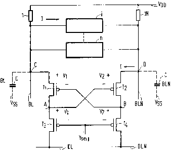
Fig. 1 shows an embodiment of a sense amplifier in
accordance with the invention. The sense amplifier comprises 4 P~OS-
transistors T1, T2, T3 and T4. The sources of the transistors T1 and T2
are connected to the first input C and the second input D, respectively,
of the sense amplifier. The junction points C and D are also connected
to bit lines BL and BLN of a memory column, which bit lines BL and BLN
are each connected to the supply terminal VDD via a load 1 and a load
1N, respectively. A number of N memory cells, only two of which are
shown in Fig. 1 for the sake of clarity, are connected to the bit lines
BL and BLN. Using known techniques, a single memory cell in a memory
column can be selected, that is to say by way of row selection
transistors which connect the bit line and the non-bit line to the
memory cell. The drain of the transistors T1 and T2 is connected to the
source of the transistors T3 arid T4, respectively, and to junction
points A and B, respectively. The drains of the transistors T3 and T4
are connected to data lines DL and DLN, respectively. The gates of the
transistors T3 and T9 receive a common selection signal YSEhj. The
selection signal YSELj selects a column j, where 1 <_ j _< m. The
gates of the transistars T1 and T2 are connected to the drains of the
transistors T2 and T1, respectively. The bit lines BL and BLN have a
parasitic bit line capacitance CBL and CBLN, respectively, shown in
parallel between respective junction points C and D and the supply
terminal VSS in Fig. 1.
The operation of the circuit shown in Fig. 1 is as
follows: the bit lines BL and BLN are first charged via the loads 1
and 1N, sa that the set voltage on the junction points C and D assumes a
value between the voltages on the supply terminals VSS and VDD (usually
approximately 4 V in the case of a supply voltage amounting to 5 V).
Consequently, the junction points A and B carry a voltage which is one
threshold voltage of the transistors T1 and T2 lower than the set
voltage on the junction paints C and D (approximately 3 V for a
threshold voltage of approximately 1 V for a set voltage of
approximately 4 V). When the selection signal YSEL is subsequently logic
low, the transistors T3 and T4 are turned on. The transistors T1, T2, T3
and T4 are proportioned so that they are all operative in the saturation
region when information on the bit lines BL and BLN is read by the sense
amplifier. For Substantially the same dimensions of the transistors T1
PHN 12.970 4 21.09.1990
and T3, and T2 and T4, respectively, the voltage differences between the
gate and the source of the transistors T1 and T3, and T2 and T4,
respectively, axe the same because of the equal currents through the
transistors T1 and T3, and T2 and T4, respectively. Fox a voltage
difference V1 and V2 between the gate and the source of the transistors
T1 and T3, and T2 and T4, respectively, the juncaion points A and B
carry a voltage V1 and V2, respectively (selection signal XSELj is logic
low). The gate of the respective transistor T1 and T2 thus carries a
voltage V2 and V1, respectively. The junction points C and D thus carry
a voltage (V1 + V2). After the selection of a single memory cell i in
the column j, either the junction point C or the junction point D will
be slightly discharged by a discharge current I, depending on the
information in the memory cell i. By way of example it is assumed in
Fig. 1 that the junction point C is slightly discharged. The voltage on
the junction point C slightly decreases due to the discharge current I.
Because the voltages on the junction points C and D, howevex, are
maintained equal by the sense amplifier in accordance with the invention
(equalization effect), the sense amplifier also decreases the voltage on
the junction point D to the same extent as the voltage decrease on the
junction point C. Said voltage decrease on the junction point D is
realised by way of a discharge current I. The difference between the
drain currents of the transistors T3 and T4 amounts to the current I,
being equal to the discharge current I of the memory cell i. Because of
the intrinsic equalization effect on the voltages on the junction points
C and D (being connected to the bit lines HL and BLN), a sense amplifier
in accordance with the invention offers the advantage that the sensing
delay of the sense amplifier is substantially independent of. the bit
line capacitance CBL or CBLN, because no or substantially no discharging
of the bit line capacitance is required fox reading the information in
the memory cell i.
Simulations performed on a sense amplifier in accordance
with the invention have demonstrated that for substantially the same
width/Iength ratios (W/L) of the transistors T1 and T3, and T2 and T4,
respectively, the voltages on the junction points A and B are not
latched to one of the voltages on the supply terminals. This offers the
advantage that a sense amplifier in accordance with the invention is
self-restoring, so that the setting of the transistor T3 or T~) will not
PHN 12.970 5 29.04.1990
leave the saturation region.
Thexe are two ways of deriving an output signal from the
sense amplifier: first of all by measurement of a voltage difference on
the junction points A and B, and secondly via a difference in currents
through the first current branch, via the transistors T1 and T3, to
the data line DL and through the second current branch, via the
transistors T2 and T4, to the non-data line DLN.
In the first case a voltage difference will occur between
the junction points A and B due to the appearance of a difference
current I through the transistors T3 and T4. For a further amplification
the junction points A and B may be connected to a further sense
amplifier stage, in which case the drains of the transistors T3 and T4
can be connected to the supply terminal VSS.
In the second case the currents through the transistors
T3 and T4 can be applied to a second amplifier stage, via the data
lines DL and DLN, .in which a current difference can be converted into a
voltage difference.
Fig. 2 shows an embodiment. of an integrated memory in
accordance with the invention which comprises several sense amplifiers
4j, 4j+1 etc, whose output signals are applied to the data lines DL and
DLN via_ mutually different currents. Elements in Fig. 2 which
correspond to elements of Fig. 1 are denoted by corresponding
references. The outputs of the sense amplifiers 4j, 4j+1 etc, are
connected to common data lines DL and DLN. The sense amplifiers 4j+1
etc. axe constructed in the same way as the sense amplifier 4j. The
memory cells i in the column j and the bit line capacitances CBL and
CBLN have been omitted in Fig. 2 for the sake of clarity, but are indeed
present in the circuit. The loads 1 arid 1N of Fig. 1 consist of NMOS-
transistors 1 which are connected as diodes. However, they may
alternatively be formed by PMOS-transistors connected as diodes. Between
each of the data lines DL and DLN and the supply terminal VSS there is
included an NMOS-transistor T15, T16, respectively, connected as a
diode. Furthermore, a further amplifier stage 20 is connected to the
data lines DL and DLN. A buffer circuit 30 is connected to output AA of
the amplifier stage 20, which buffer circuit produces an output signal
on output BB.
The operation of the circuit shown in Fig. 2 is as
PHN 12.970 6 24.04.1990
follows: after the selection of a single desired sense amplifier 4j in a
memory column j by means of a selection signal YSELj, the information is
transferred from a selected memory cell i in the relevant column j to
the data lines DL and DLN by way of currents which are mutually
different. The currents through the data lines DL and DLN are applied to
the supply terminal VSS by means of the transistors T15 and T16, said
currents being converted into voltages because of the diode effect of
T15 and T16. Because the value of the currents through the data lines DL
and DLN differs (i.e. the current I), different voltages are applied to
the inputs of the further amplifier stage 20. The input signals are
further amplified in the amplifier stage 20 and applied, via the
output AA, to a buffer circuit 30. The buffer circuit 30 outputs an
output signal having CMOS output levels on the output BB.