Note: Descriptions are shown in the official language in which they were submitted.
"' ~4i "'~"~ c~. ~
~~~. :~. fit: ..
P~IQ 89.018 1 14.05.1990
Digital transmission system using subband coding of a digital signal.
The invention relates to a digital transmission system
having a transmitter and a receiver, the transmitter including a coder
and the receiver including a decoder, for subband coding of a digital
signal, such as a digital audio signal, having a given sampling rate
FS, the coder being responsive to the digital signal, for generating a
number of M sub-band signals with sampling rate reduction, the coder
dividing the digital signal band into successive subbands of band
numbers m(1 < m _<M) increasing with frequency, the decoder being
responsive to the M subband signals for constructing a replica of the
digital signal, this decoder merging the subbands to the digital signal
band, with sampling rate increase.
The invention also relates to a transmitter and a receiver for use in
the transmission system, a coder for use in the transmitter, a decoder
for use in the receiver, an analysis filter for use in the coder, a
synthesis f.iltex for use in the decoder, and a digital audio signal
recording or reproducing apparatus comprising the transmitter and the
receiver respectively.
A system for subband coding is known from the article
entitled "The critical Band Ooder - Digital encoding of speech signals
based on the perceptual requirements of the auditory system" by M.E.
Krasner, Froc. IEEE ICASSP80, Vol. 1, pp. 327-311, April 9-11, 1980. In
this known system, use is made of a subdivision of the speech signal
band into a number of subbands, whose bandwidths approximately
correspond with the bandwidth of the critical bands of the human
auditory system in the respective frequency ranges (compare fig. 2 in
the article by Krasner). This subdivision has been chosen because on the
basis of psycho acoustic experiments it may be expected that in a such
like subband the quantization noise will be optimally masked by the
signals within this subband when the quantizing takes account of the
noise masking curve of the human auditory system (this curve indicates
the threshold far masking the noise in a critical band by a single tone
in the centre of the critical band, compare fig. 3 in Krasner~s
CA 02017841 1999-09-16
- 2 -
article.
The invention has for its object to provide a digital
transmission system in which the information transmitted via
the transmission medium between the transmitter and the
5receiver is divided in subbands having all approximately the
same bandwidth, and which is constructed such that practically
not distortion because of aliasing occurs in the reconstructed
signal at the receiver side, and where the coder and decoder
are very efficient with respect to computation time and
locomplexity of the circuitry needed.
According to the invention there is provided:
a digital transmission system having a transmitter
and a receiver, the transmitter including a coder and the
receiver including a decoder, for subband coding of a digital
i5signal, such as a digital audio signal, having a given sampling
rate FS, the coder being responsive to the digital signal, for
generating a number of M subband signals with sampling rate
reduction, the coder dividing the digital signal band into
successive subbands of band numbers m(1<m<M) increasing with
2ofrequency, the decoder being responsive to the M subband
signals for constructing a replica of the digital signal, this
decoder merging the subbands to the digital signal band, with
sampling rate increase, wherein the coder comprises analysis
filter means and a signal processing unit, the analysis filter
25means comprises M analysis filters each having one input and
two outputs, the 2M outputs of the filters being coupled to 2M
outputs of the analysis filter means for supplying 2M output
signals with a sampling rate FS/M, each analysis filter being
adapted to apply two different filterings on the signal applied
3oto its input and to supply each of the two different filtered
versions of that input signal to a corresponding one of the two
outputs, each one of the 2M filter outputs being coupled to a
corresponding one of 2M inputs of a signal processing unit, the
processing unit having M outputs coupled to M outputs of the
35coder for supplying the M subband signals, the signal
CA 02017841 1999-09-16
- 3 -
processing unit being adapted to supply output signals on each
of M outputs, an output signal being a combination of at least
a number of input signals applied to its 2M inputs, the decoder
comprises another signal processing unit and synthesis filter
5means the other signal processing unit having M inputs for
receiving the M subband signals and having 2M outputs, the
synthesis filter means comprising M synthesis filters each
having two inputs, and one output coupled to the decoder
output, the other signal processing unit being adapted to
logenerate an output signal on each of its 2M outputs, an output
signal being a combination of at least a number of input
signals applied to its M inputs, each pair of outputs of the
other signal processing unit being coupled to a pair of two
inputs of a corresponding one of the M synthesis filters, each
i5synthesis filter having one output, each synthesis filter being
adapted to apply different filterings on the two signals
applied to the two inputs and to supply a combination of the
two filtered signals to its output, each output can be coupled
to the output of the synthesis filter means for supplying the
2oreplica of the digital signal having a sampling rate Fs, in that
the coder is adapted to divide the digital signal band into
successive subbands having approximately equal bandwidths,
characterized in that the coefficients of each of the analysis
and synthesis filters are derived from the coefficients of a
25standard filter having a low pass filter characteristic with a
bandwidth approximately equal to half the bandwidth of the
subbands, and that the coefficients for the analysis filters
and the synthesis filters are derived from a standard filter
having an odd number of coefficients, that M is an even number
3oand that for making the number of coefficients of the standard
filter equal to the number of multiplication factors of each of
the analysis and synthesis filters, zeroes are added to the
array of coefficients of the standard filter.
The measures according to the invention are based on
35the recognition that computation can be greatly simplified by
CA 02017841 1999-09-16
- 3a -
arranging a sample rate decreaser in the form of the first unit
before the analysis filters in the transmitter and by arranging
a sample rate increaser in the form of the second unit behind
the synthesis filters in the receiver, in that the computations
5are now applied on signals with a lower sampling rate. It
should be noted that the publication "Digital filtering by
polyphase network: application to sample-rate alteration and
filter banks" by M.G. Bellanger et al in IEEE Trans. on ASSP,
Vol. 24, No. 2, April 1976, pp. 109-114 discloses a system in
iowhich a digital signal is divided into a number of subbands by
means of a number of filters, the said filters being preceded
by a sample rate decreaser. Such a construction simplifies
computation in the filters in that signal processing in these
filters can be applied to signals having a decreased sampling
i5 rate .
The transmitter in the known system however does not
generate subbands of substantially equal bandwidths, in that
the lowest subband in the known system has a bandwidth of half
the bandwidth of the other bandwidths. Moreover the filters
2oand the processing unit in the known system differ from the
filters and the processing unit in the system according to the
invention in that the filters apply two different filterings on
the signals applied to their inputs instead of one, such as in
the known system. This makes the content of the information
25transfer between the filters and the processing unit according
to the invention twice of that in the known system. This makes
it possible, by making use of a proper choice for the filter
coefficients in the filters, as well as by choosing an
appropriate construction of the processing units at the
3otransmitter and the receiver side, to realize a reconstructed
signal at the receiver side that is
~w(1 "~, f t~: "~.
PHQ 89.018 4 14.05.1990
practically devoid of any distortion because of aliasing. Contrary to
this, the reconstructed signal in the known system is always subject to
aliasing distortion, even for the most optimal construction of the
filters and the processing units.
Preferably the coefficients for the analysis filters and
synthesis filters are dexived from a standard filter having an odd
number of coefficients. This leads to a significant reduction in
computations in the (other) processing unit, in that, in that case,
there is a large symmetry in the coefficients for the (other) processing
unit.
Various embodiments of the analysis and synthesis
filters are possible.
In one embodiment the system on the transmitter side may
be characterized in that each analysis filter comprises a series
arrangement of delay sections having equal delay (T), the input of the
filter being coupled to the input of the first delay section, outputs of
at least a number of odd numbered delay sections in the series
arrangement being coupled to corresponding inputs of a first signal
combination unit, outputs of least a number of even numbexed delay
sections in the series arrangement being coupled to corresponding inputs
of a second signal combination unit, outputs of the first and second
signal combination unit being coupled to the first and second output
respectively of the filter. Preferably, the outputs of add numbered
delay sections being coupled to inputs of the first signal combination
unit only, and outputs of even numbered delay sections are coupled to
inputs of the second signal combination unit only. In another
embodiment, the system may be characterized in that each analysis :filter
comprises two series arrangements of delay sections having equal delay
(2T), the input of the filter being coupled to the inputs of the first
and at least a number of other delay sections in each series
arrangement, the outputs of the two series arrangements being coupled to
the first and second output of the filter respectively, a further delay
section having a delay (T) that equals half the delay of the delay
sections in the series arrangements, being coupled in the signal path
from the input to the second output of the filter, the said further
delay section not being included in the signal path from the inputto the
first output of the filter.
~,T1 ~ r"'y'~,1 .~I
. ~C.~,~
PHQ 89.018 5 14.05.1990
One the receiver side, the system may be characterized
in that each synthesis filter comprises two series arrangements of delay
sections, having equal delay (2T), the first and second inputs of the
filter being coupled to an input of the first delay section of the first
and second series arrangement respectively, outputs of at least a number
of delay sections in the first series arrangement being coupled to
corresponding inputs of a signal combination unit, outputs of at least a
number of delay sections in the second series arrangement also being
coupled to corresponding inputs of the signal combination unit, an
output of the signal combination unit being coupled to the filter
output, a further delay section having a delay (T) that equals half the
delay of the delay sections in the series arrangements, being coupled in
the signal path from the second input to the output of the filter, the
said further delay section not being included in the signal path from
the first input to the output of the filter.
Tn another embodiment, the system may be characterized in that
that each synthesis filter comprises a series arrangement of delay
sections having equal delay (T), the first input of the filter being
coupled to inputs of at least a number of odd numbered delay sections in
the series arrangement, the second input of the filter being coupled to
inputs of at least a number of even numbered delay sections in the
series arrangement, the output of the last delay section being coupled
to the output of the filter. Preferably, the first filter input is
coupled to inputs of odd numbered delay sections only, and the second
filter input is coupled to inputs of even numbered delay sections
only.
also various embodiments of the signal processing unit in
the transmitter and the other processing unit in the receiver are
possible. In one embodiment the signal processing unit comprises l~!
signal combination units, each having an output coupled to a
corresponding one of the M outputs of the signal processing unit, in
that for each signal combination unit, at least a number of inputs of
the 2M inputs of the processing unit are coupled to corresponding inputs
of the said signal combination unit, via corresponding multiplication
units. The corresponding other signal processing unit on the receiver
side then comprises 2M signal combination units, each having an output
coupled to a corresponding one of the 2M outputs of the processing unit,
CA 02017841 1999-09-16
- 6 -
in that, for each signal combination unit, at least a number of
inputs of the M inputs of the processing units are coupled to
corresponding inputs of the said signal combination unit, via
corresponding multiplication units.
s On the transmitter side the system may be further
characterized in that the two outputs of each analysis filter
are each coupled to their corresponding inputs of the signal
processing unit via a corresponding signal amplification unit,
both amplification units being adapted to amplify the signals
ioapplied to their inputs by the same complex value, the complex
values preferably being different for amplification units
coupled to different analysis filters. In addition each output
of the processing unit may be coupled to its corresponding
output of the coder via a series arrangement of a signal
i5amplification unit and real value determinator, the signal
amplification unit being adapted to amplify the signal applied
to its input by a complex value.
On the receiver side, the system may be further
characterized in that the two outputs of each pair of outputs
2oof the other signal processing unit are each coupled to their
corresponding input of a synthesis filter via a corresponding
signal amplification unit, both amplification units being
adapted to amplify the signals applied to their inputs by the
same complex value, the complex values preferably being
25different for amplification units coupled to different
synthesis filters.
In addition the M inputs of the decoder may be
coupled to their corresponding one of the M inputs of the other
processing unit via a signal amplification unit, the signal
3oamplification unit being adapted to amplify the signal applied
to its input by another complex value.
The invention may also be summarized as:
a coder for subband coding of a digital signal, such as a
digital audio signal, having a given sampling rate Fs, the
35coder being responsive to the digital signal band into
CA 02017841 1999-09-16
- 6a -
successive subbands of band numbers m(l~rrLM) increasing with
frequency, the coder comprising analysis filter means and a
signal processing unit, the analysis filter means comprises M
analysis filters each having one input and two outputs, the 2M
5outputs on the filters being coupled to 2M outputs of the
analysis filter means for supplying 2M output signals with a
sampling rate Fs/M, each analysis filter being adapted to apply
two different filterings on the signal applied to its input and
to supply each of the two different filtered versions of that
loinput signal to a corresponding one of the two outputs, each
one of the 2M filter outputs being coupled to a corresponding
one of 2M inputs of a signal processing unit, the processing
unit having M outputs coupled to M outputs of the coder for
supplying the M subband signals, the signal processing unit
i5being adapted to supply output signals on each of M outputs, an
output signal being a combination of at least a number of input
signals applied to its 2M inputs, wherein the coder is adapted
to divide the digital signal band into successive subbands
having approximately equal bandwidths, characterized in that
2othe coefficients of each of the analysis filters are derived
from the coefficients of a standard filter having a low pass
filter characteristic with a bandwidth approximately equal to
half the bandwidth of the subbands, that the coefficients for
the analysis filters are derived from a standard filter having
25an odd number of coefficients and that the coefficients for the
analysis filters are derived from a standard filter having an
odd number of coefficients, that M is an even number and that
for making the number of coefficients of the standard filter
equal to the number of multiplication factors of each of the
3oanalysis and synthesis filters, zeroes are added to the array
of coefficients of the standard filter.
According to another aspect the invention provides:
a decoder for decoding M subband signals that have been
obtained by subband encoding a digital signal by dividing the
35digital signal band in approximately equal bandwidths, the
CA 02017841 1999-09-16
- 6b -
decoder being responsive to the M subband signals for
constructing a replica of the digital signal, this decoder
merging the subbands to the digital signal band, with sampling
rate increase, the decoder comprising a signal processing unit
sand synthesis filter means the signal processing unit having M
inputs for receiving the M subband signals and having 2M
outputs, the synthesis filter means comprising M synthesis
filters each having two inputs, and one output coupled to the
decoder output, the other signal processing unit being adapted
loto generate an output signal on each of its 2M outputs, an
output signal being a combination of at least a number of input
signals applied to its M inputs, each pair of outputs of signal
processing unit being coupled to a pair of two inputs of a
corresponding one of the M synthesis filters, each synthesis
i5filter having one output, each synthesis filter being adapted
to apply different filterings on the two signals applied to the
two inputs and to supply a combination of the two filtered
signals to its output, each output can be coupled to the output
of the synthesis filter means for supplying the replica of the
2odigital signal having a sampling rate Fs, characterized in that
the coefficients of each of the synthesis filters are derived
from the coefficients of a standard filter having allow pass
filter characteristic with a bandwidth approximately equal to
half the bandwidth of the subbands and that the coefficients
25for the synthesis filters are derived from a standard filter
having an odd number of coefficients and that the coefficients
for the synthesis filters are derived from a standard filter
having an odd number of coefficients, that M is an even number
and that for making the number of coefficients of the standard
3ofilter equal to the number of multiplication factors of each of
the analysis and synthesis filters, zeroes are added to the
array of coefficients of the standard filter.
The invention will now be explained further with
reference to a number of embodiments in the following figure
35description. The figure description discloses in
CA 02017841 1999-09-16
- 6c -
figure 1 an embodiment of the transmission system in
accordance with the invention, in the form of a block diagram,
figure 2 the realization of the sample rate increase
by means of the first unit,
s figures 3 and 4 two embodiments of the analysis
filter in the system,
figures 5 and 6 two embodiments of the synthesis
filter in
~r~~~~ ~ ~.-,~'»:r r
. a'C.:
..
- 7 - 2010-8632
the system,
figure 7 an embodiment of the signal processing unit in
the transmitter or the other signal processing unit in the
receiver,
figure 8 another embodiment of the transmitter in the
system,
figure 9 another embodiment of the receiver in the
system,
figure 10 the derivation of the coefficients of the
analysis filters in the receiver,
figure 11 another example of the processing unit in the
transmitterr or the other signal processing unit in the
receiver,
figure 12 a digital signal recording apparatus,
figure 13 a digital signal reproduction apparatus, and
figures 14 to l9 are Tables I 'to VI which list co-
efficients for various processing units arid filters.
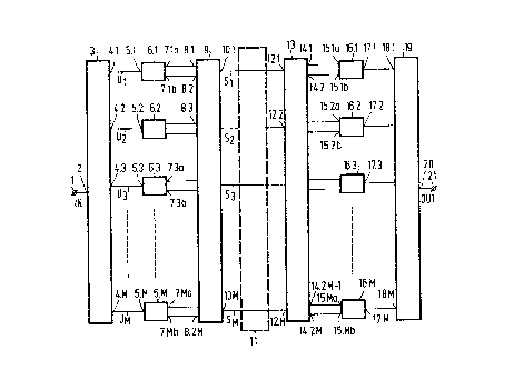
Figure l discloses a block diagram of the digital
transmission system. The system has an input terminal 1 coupl2d
to an input 2 of a first unit 3, for receiving a digital system
IN having a given sampling rate Fg. The first unit has M out-
puts 4.1 to 4.M on which output signals Ul to UM are avail-
able. The first unit 3 is adapted to realize a sample rate
decrease by a factor M on the input signal IN applied to its
input 2. The functioning of the first unit 3 will be explained
later with reference to figure 2. M analysis filters 6.1 to 6.M
~ (.~J-~.r;~"~~~,,eM ~!.
- '7a - 20104-8632
are present, each analysis filter m having an input 5.m coupled
to a corresponding one (4.m) of the M outputs of the first unit
3. m runs from 1 to M. Each analysis filter 6.m has two outputs
7. ma and 7.mb. Each analysis filter (6.m) is adapted to apply
two different filterings on the signal (Um) applied to its
input (5.m) and to supply each of the two different filtered
versions of that input signal (Um) to a corresponding one of
the two outputs (7.ma and 7.mb). The construction and the
functioning of the analysis filters will be explained later with
reference to the figures 3, 4 and 10. Each ane of the 2M filter
outputs 7.1a, 7.1b, 7.2a, 7.2b, ..., 7.ma, 7.mb, ..., 7Ma, 7Mb
are coupled to a corresponding one of 2M inputs 8.1, 8.2, ...,
8M, 8M+l, ..., 8.2M of a signal processing unit 9. The
processing unit 9 has M outputs to 10.1 to 10. M. The processing
unit 9 is adapted to supply different output signals on each of
its M outputs, an output signal being a combination of at least a
number of input signals applied to its 2M inputs.
~n~.'~. f~t~~.~~1 ~.
PHA 89.018 8 14.05.1990
The construction and functioning of the signal processing
unit 9 will be explained later with reference to the figures 7 and 8. If
the outputs 10.1 to 10.M are identical to the M outputs of the filter
means, then this means that the signal processing unit 9 supplies the M
subband signals S1 to SM, each subband signal Sm being available
on a corresponding one (10.m) of the M outputs of the processing unit 9.
The input signal IN applied to the input 1 and having a
sampling rate of Fs, occupies a bandwidth equal to FS/2. Division of
the signal bandwidth by a factor of M this means that the bandwidth of
the subbands 81 to HM all equal FS/2M, see figure 10c, s1 in
figure 1 being a down sampled version of the signal present in subband
B1, s2 being a down sampled version of the signal present in
subband B2, etc.
The M subband signals can, if necessary, further be
processed, e.g. in an additional quantizer (not shown), in which an
(adaptive) quanti2ation can be applied on the signals in order to
realise a significant reduction in bit rate. Examples of such quantizers
can e.g. be found in the published European patent application
No. 289.080 (PHN 12.108).
The signal processing described above is carried out on
the transmitter side of the transmission system. The transmitter in the
system thus at least include the elements with reference numerals 3, 6.1
to 6.M and 9, and, it picesent , the quantizer.
The signals generated in the transmitter are supplied via
a transmission medium, schematically indicated by reference numeral 11
in figure 1, to the receiver. This might make the application of a
further channel coding of the signal necessary, in order to make an
error correction possible at the receiver side. The transmission via the
transmission medium 11 can be in the form of a wireless transmission,
such as e.g. a radiobroadcast channel. However also other media are well
possible. One could think of an optical transmission via optical fibres
or optical discs, or a transmission via magnetic record carriers.
The information present in the M subbands can be
transmitted in parallel via the transmission medium, such as is
disclosed in figure 1, or can be transmitted serially. In that case time
compression techniques are needed on the transmitter side to convert the
parallel data stream into a serial data stream, and corresponding time
14.05.1990
PHA 89.018
expansion techniques are needed on the receiver side to reconvert the
data stream into a parallel date stream, so that the M subband signals
S1 to SM can be applied to respective ones of the M inputs 12.1 to
12.N1 of another processing unit 13. The processing unit 13 has 2M
outputs 14.1 to 14.2M. The other signal processing unit 13 is adapted to
generate an output signal on each of its 2M outputs, an output signal
being a combination of at least a number of input signals applied to its
M inputs.
The construction and functioning of the other signal
processing unit 13 will be explained later with reference to the figures
7 and 9. Pairs of outputs, such as 14.1 and 14.2, of the other
processing unit 13 are coupled to pairs of inputs, such as 15.1a and
15.1b, of a corresponding one of M synthesis filters 16.1 to 16.k~1. Each
synthesis filter 16.m has one output 17,m. The synthesis filters are
applied to apply different filterings on the two signals applied to
their two inputs and to supply a combination of the two filtered signals
to their output. The construction and functioning of a synthesis filter
will be explained latex with reference to the figures 5, 6 and 14. The
output (17.m) of each synthesis filter (16.m) is coupled to a
corresponding one (18.m) of M inputs 18.1 to 18.M of a second unit 19.
An output 20 of the second unit is coupled to an output 2'f of the
transmission system. The functioning of the second unit 19 will be
explained later with reference to figure 2.
The receiver in the system includes at least the elements
with reference numerals 13, 17.1 to 17.M and 19.
If the subband signals have been quantized at the
transmitter side, a corresponding dequantizer will be needed in the
receiver. Such a dequantizer should be coupled before the other signal
processing unit 13. Examples of such dequantizers can also be found in
the previously mentioned European patent application No. 289.080. The
signal processing at the receiver side need to be such that signals u1
to um are present at the outputs of the synthesis filters 16.1 to
16. M, and that a reconstructed signal OUT is present at the output
terminal 21 which, in the ideal case, equals the input signal IN,
applied to the input terminal 1.
Figure 2 discloses the functioning of the first and
second units 3 and 19 respectively. The signal IN applied to the input
. r ~.: .
PHQ 89.018 10 14.05.1990
terminal 1 is given schematically in figure 2(a) as a function of time.
Figure 2a discloses the samples from which the input
signal IN is built up. It discloses only the location of 'the samples in
time, not the amplitude of the samples. The samples are located a time
interval T1, which equals 1/FU, apart. The sampling rate of the
input signal thus equals FS. In the example of figure 2, it is assumed
that M equals 8. The signals given in figure 2b to 2i (again only the
locations in time, not the amplitudes axe given) disclose the signals
U8 to U1 present at the outputs 4.1 to 4.8 respectively of the unit
3. The unit 3 acts in fact as a commutator in that it distributes the
each time eight samples contained in consecutive imaginary blocks
cyclically to the eight outputs, see also the commutator 3 in figure 8.
From figure 2 it is clear that the output signals
available at the M outputs of the unit 3 have a sampling rate of FS/M.
The samples in the output signals are now spaced a time interval T,
which equals M.T1, apart.
The reconstruction of 'the output signal OUT in the second
unit 19 will be explained hereafter. The unit 19 can also be considered
to be a commutator, in that it cyclically couples each of the M inputs
18.1 to 18.8 with the output 20. In this case, samples occur after each
other at the inputs 18.1 to 18. M, in this order, and are applied to 'the
output 20 by the commutator 19. This is shown more clearly by the
commutator 19 in figure 9.
The first unit can also be built up in a different way,
namely by making use of a delay line having toppings at the correct
locations along the said delay line. These toppings are then coupled to
inputs of decimators, that bring the sampling rate down to the correct
value.
It is even possible to combine the first unit and the analysis filters,
expecially by making use of the delay line in the first unit for (a part
of) the delay lines) in the analysis filters, which is well known in
the art.
The same reasoning is in fact valid for the second unit 19.
In this case interpolators are needed in order to realise the sample
rate increase.
Figure 3. discloses a first embodiment of an analysis
filter 6.m. An input 30 of the analysis filter, which equals the input
79
~~; ( 1: ,~
Wr ...~ a,
PHQ 89.018 11 14.05.1990
5.m in figure 1, is coupled to a series arrangement 31 of delay
sections, having equal delays T. Outputs of the odd numbered delay
sections 32.1, 32.3, ..., 32.n are coupled to inputs of a first signal
combination unit 33. Outputs of the even numbered delay sections 32.2,
32.4, ..., axe coupled to inputs of a second signal combination unit
34. Outputs of the first and second combination units 33 and 34 form the
first and second output 35.1 and 35.2 respectively of the analysis
filter 6.m. They equal the outputs 7.mb and 7.ma, respectively in fig. .
1. The input 30 of the filter 6.m is coupled to an input of the second
signal combination unit 34 via a multiplication unit 36.1. This
multiplication unit multiplies the signals (samples) applied to its
input by a factor of aom. The outputs of the odd numbered delay
sections axe coupled to the inputs of the signal combination unit 33 via
multiplication units 36.2, 36.4, ..., 36.n-1 and 36.n*1. They multiply
the signals (samples) applied to their respective units by respective
factors of alm, aim, ..., anm. The outputs of the even numbered
delay sections axe coupled to the inputs of the signal combination unit
34 via multiplication units 36.3, 36.5, ..., 36.n. They multiply the
signals (samples) applied to their respective inputs by respective
factors of a2m, a4m, ... Tn a more general definition of the signal
combination units, these multiplication units can be considered as being
included in the signal combination units. In that case, the signal
combination units not only realize a summation of the signals applied to
their inputs, but they realize a weighted combination (summation) of
these signals. It is evident that, in the case that a multiplication
unit has a factor aim that equals zero, the coupling from the delay
section to the signal combination unit including the said multiplication
unit is dispensed with. It is further evident that, in the case that the
said multiplication unit has a factor aim 'that equals one, the
multiplication unit is dispensed with, so that the coupling is a direct
coupling.
Figure 4 shows another embodiment for the analysis filter
6.m. Although the circuit construction of the filter in figure 4 is
different from the circuit construction of the filter of figure 3, it
can carry out the same functioning and the same filterings, when some
conditions are met. The filter of figure 4 includes two series
arrangement 40 and 41 of delay sections having equal delay (2T). The
~~~ "~, f'~ l° '~,
PHQ 89.018 12 14.05.1990
input 30 of the filter is coupled to inputs of the delay sections in the
series arrangement 40 via multiplication units 42.1 to 42.p-1
respectively and with the output 35.2 of the filter via a multiplication
unit 42. p. That means that the series arrangement 40 includes p-1 delay
sections 44.1 to 44.p-1. The input 30 of the filter is further coupled
to inputs of the delay sections in the series arrangement 41 via
multiplication units 4.1 to 43.q-1, and further with the output 35.1 of
the filter via a multiplication unit 43. q. That means 'that the series
arrangement 41 includes q-1 delay sections 45.1 to 45.q-i. The
multiplication units 42.1 to '12.p multiply their input signals by a
factor blm, b2m, ..., bpm respectively. The multiplication units
43.1 to 43.q multiply their input signals by a factor clm, ..., cqm
respectively. Signal combination units 46.1 to 46.p-1 are coupled to 'the
outputs of the delay sections 44.1 to 49.p-1 of the series arrangement
40. Signal combination units 47.1 to 4T.q-1 are coupled to the outputs
of the delay sections 45.1 to 45.q-1 of the series arrangement 41. The
output of the combination unit 47.q-1 is coupled to the filter output
35.1 via an additional delay section 48 having a delay T that equals
half the delays of the delay sections in the Series arrangements. The
delay section 4H could have been provided somewhere else in the signal
path from the input 30 to the output 35.1, provided that this delay
section is not included in the signal path from the input 30 to the
output 35.2.
What has been said with reference to figure 3 in the case
that a multiplication unit has a multiplication factor that equals one
or zero, is of course also valid in this case. Tn the latter case, let
us assume that b2m would be zero, this also means that the
corresponding signal combination unit 46.1 that would otherwise have
been coupled to the output of the relevant multiplication unit 42.2 can
also be dispensed with. This means that the delay section 44.1 is
directly connected to to delay section 44.2, or they can be combined
into a delay section having a delay of 4T.
Under certain conditions the filter of figure 4 functions
the same and realizes the same filterings on the input signal, as the
filter of figure 3. The conditions for this are:
p=q=(n+1?/2, bpm aom, Cq~ alm, bp-1.m a2m~ cq-1.m=a3m~
..., b1m an_1.m and c1m anm~
PHQ 89.018 13 19.05.1990
In this case, it is assumed that n is an add number. If, however n is an
even number, the number of couplings to the combination unit 34 in
figure 3 is one larger than the number of couplings to the combination
unit 33. In that case the conditions are as follows:
q=p-1=n~2, bpi aom, cqm a1m° bp-1.m-a2m° Cq-l.m~a3m'
..., blm~anm and c1m=an_1,m'
Please note that the coupling including the multiplication unit 36.n+1
in the filtex of figuxe 3, where n is even, is a coupling from the
output of the series arrangement 31 to the signal combination unit 34!
Figure 5 shows a synthesis filter 16.m having two inputs
50.1 and 50.2 and one output 51. The inputs equal the inputs i5.ma and
15.mb and the output equals the output 17.m in fig. 1.
The synthesis filter includes two series arrangements 52 and 53 of delay
sections having equal delay 2T. The filter 16.m further includes a
signal combination unit 54 and an additional delay section 55 having a
delay T that equals half the delay of the delay sections in the
arrangements. The inputs 50.1 and 50.2 are coupled to inputs of the
signal combination unit 54 via multiplication units 56.1 and 57.1
respectively. The series arrangement 52 includes p-1 delay sections 58.1
to 58.p-1. Outputs of these delay sections are coupled to corresponding
inputs of the combination unit 54 via corresponding multiplication units
56.2 to 56. p. The multiplication units 56.1 to 56.p multiply their input
signals by a factor of d1m to dpm respectively. The sexies
arrangement 53 includes q-1 delay sections 59.1 to 59.q-1. Outputs of
these delay sections are coupled to corresponding inputs of the
combination unit 54 via corresponding multiplication units 57.2 to
57. q. The multiplication units 57.1 to 57.q multiply their input signals
by a factor of elm to eqm respectively. The output 60 of the
combination unit 54 is coupled to the filter output 51. The delay
section 55 is included between the input 50.2 and the input of the
series arrangement 53. More generally, the delay section 55 can be
included somewhere in the signal path from the input 50.2 to the output
51 such that it is not included in the signal path from the input 50.1
to the output 51.
For the filter 16.m to apply the correct filterings at
the receiver side on the two signals applied to the inputs 50.1 and
50.2, when the m-th filter on the transmitter side is the filter 6.m of
.... . ~ b .
PHA 89.018 14 14.05.1990
figure 3, the following condition should be met:
p=q=(n+1)/2. d1m=aom~ elm=a1m~ d2m=a2m~ e2m=a3m~ ...,
dpm an_1.m and eqfi anm. Agaa.n it is assumed that n is an odd
number. In the same way as explained previously it can be found that for
n is an even number, the conditions a.re as follows:
q=p_1=n/2~ d1m=aom, elm=alm, d2m=a2m~ e2m=aim, ...,
eq~ an_1.m and dpm=an. m'
Figure 6 shows another embodiment of the synthesis filter
16.m, denoted by 16.m'. The filter includes a series arrangement 65 of
delay sections 66.1 to 66.n, having equal delay T. The input 50.1 is
coupled to inputs of even numbered delay sections, via multiplication
units 67.2, 67.4, ..., 67.n+1, n is thus considered to be an odd
number. The input 50.2 is coupled to inputs of odd numbered delay
sections via multiplication units 67,1, 67,3, ..., 67.n. Tn oxder. for
the filter 16. m' to carry out the correct filterings at the receiver
side on the signals applied to the inputs 50,1 to 50.2, when 'the m-th
filter on the transmitter side is the filter 6m of figure 3, the
coefficients with which the multiplication units 67.1 to 67.n+1 multiply
their input signals, should be as given in figure 6. These coefficients
thus equal anm, an_1.m' ' '' ~'2m~ alm~ aom respectively.
The choice for the coefficients aom to anm for the
filter 6.m of figure 3 will be further explained with reference to
figure 10.
Figure 10(c) shows the the filterband of the digital
signal, which is F$/2 Hz broad. The total filterband is divided into M
subbands B1 to BM of equal bandwidth FS/2M. Figure 10(a) shows an
imaginary or standard low pass filter having a filter characteristic of
H(f) and a bandwidth FB equal to half the bandwidth of the subbands.
Figure 10(b) shows the impulse response of the low pass filter H(f) as a
function of time. This impulse response is in the form of an array of
impulses at equidistant time intervals T1=1/Fs spaced apart. The
impulse response is characterized by an array of values h0, h1,
h2, ... indicating the amplitude of the impulses at the time intervals
t = 0, T1, 2T1, ......
Figures 10(d) to (g) show how the multiplication factors
for the multiplication units in the filters 6.1 to 6.M can be obtained
using the impulse response of the standard low pass filter H(f). As can
r
PHQ 89,018 15 19.05.1990
be seen the factors a01 to aoM, being the multiplication factors for
the multiplication units 36.1 in the filters 6.1 to 6.M, see Figure 3,
equal h0 to hM-1 respectively. The factors all to alM, being
the multiplication factors for the multiplication units 36.2 in the
filters 6.1 to 6.M, see Figure 3, equal hM to h2M_1 respectively, the
factors a21 to a2M equal -h2M to -h3M-1 respectively, the
factors a31 tn a3M equal -h3M to -h4M-1 respectively and so on,
see especially the filter in Fig. 10d, which filter is worked out a
little bit further. Preferably, the standard filter H(f) has an odd
number of impulses. This means that the filter has an odd number of
coefficients h0, h1, h2, ... The advantage of this will be made
clear later.
Figure 7 shows an embodiment of the processing unit 9.
The processing unit 9 includes X signal cambination units 70.1 to 70.X.
Y inguts, 71.1 to 71.Y, of the signal processing unit 9 are coupled via
corresponding multiplication units 72.11 to 72.1Y to corresponding
inputs of the combination unit 70.1. The Y inputs of the processing unit
are also coupled to inputs of the combination unit 70.2, via
corxesponding multiplication units 72.21 to 72.2X. This goes on for all
the other combination units 70.x, where x runs from 1 to X inclusive.
This means that the y-th input 71.y is coupled to a corresponding input
of the x-th combination unit 70.x via a corresponding multiplication
unit 72.xy, where y runs from 1 to Y. It will be cleax that Y equals 2M
and the X equals M. The inputs 71.1 to 71.2M correspond in that order
with the inputs $.1 to 8.2M in figure 1. The outputs 74.1 to 74.M in
that order correspond with the outputs 10.1 to 10.M in figure 1. The
multiplication units 72.11 to 72.1Y, 72.21 to 72.2Y, 72.31 to 72.3Y,
... 72.X1 to 72.XY multiply their input signals by a factor of crll to
alY, a21 to a2Y, a31 to a3Y, ... , aX1 to aXY
respectively. The factors axy can be calculated, using the following
formula:
cos ~p for y being an odd number
axy =
sin ~p for y being an even number
with ~ _ (-1)x-1 tt(x-1/2) (1/2-(y-1)/DIV2/M)
In the foregoing it is .assumed that the impulse response
PHQ 89.018 16 14.05.1990
of the standard filter H(f) in figure 10b has an odd number of impulses,
and thus an odd number of coefficients.
Figure 7 will also be used for explaining the
construction and functioning of the other processing unit 13 on the
receiver side. In that case, Y equals M and X equals 2M. Tn this case
the inputs 71.1 to 71.M, in that order, correspond to the inputs 12.1 to
12.M in figure 1 and the outputs 74.1 to 74.2M, in that order,
correspond to the outputs 14.1 to 14.2M in figure 1. The factors axy
for the processing unit 13 can be calculated, using the following
formula:
- ~ sin ~p' for x being an odd number
~xy
-cos gyp' for x being an even number
with ~p'=(-1)y-1tt(y-1/2)(1J2-(x-1)DIV2/M)
for an odd number of coefficients in the impulse response of H(f) in
Fig. 10b.
8y using these coefficients axy in the processing units on the
transmitter and the receiver side, one realizes a transmission system
that is practically fully devoid of any aliasing distortion. This in
fact also requires bandwidth constraints imposed on the frequency
transfer function of the standard filter. Preferably, the transition
bandwidth of the said filter should not exceed Fs/4M. A numerical
example is given in the table I for the coefficients for the processing
unit 9 and in table II for the coefficients for the other processing
unit 13, where M has been taken equal to 8, with the assumption that the
impulse response H(f) in Fig. 10b has an odd number of coefficients.
Table III includes the corresponding filter coefficients for the eight
analysis filters 6.m. The coefficients for the corresponding synthesis
filters 16.m can be derived from the coefficients in table III, in the
way as explained with reference to Figures 5 and 6. Further the tables
IV and V g~.ve the coefficients axy for the processing unit 9 and the
other processing unit 13 and table VI the coefficients a for the eight
analysis filters 6.m, in the case that the impulse response of the
standard filter H(f) includes an even number of coefficients.
From table I and II, for the situation where the standard filter has an
odd number of coefficients, it is clear that there is a large symmetry
in the coefficients fox the processing units. A large number of
~~ ~ f'~".~ f9.'~.
pHQ 89.018 17 14.05.1990
coefficients in one table is equal to each other, or differ only by its
sign. This makes a large reduction in multiplying capacity possible.
This contrary to the tables IV and V, for the situation where the
standard filter has an even number of coefficients. Here the
coefficients differ much more from each other.
As already explained, table III includes the filter coefficients derived
from a standard filter having an odd number of impulses in the impulse
response function. This is a filter that generates 127 impulses upon
application of one input impulse, and which filter includes 127 filter-
coefficients. The table however includes 128 coefficients. This has been
realized by adding one zero as the first coefficient h0, see the value
for a01 in table III. Table VI has been obtained from a standard
filter having an even number of (128) coefficients. In both cases, the
impulse response of the standard filter are symmetrical. That means that
two coefficients lying symmetrically around the middle are equal, except
fox their signs. This middle is for the odd numbered case at the
location in time of the impulse h64. This means that h1(=a0,2)
equals h.~27 (=a16,8)~ h2 (=a0.3) equals h126 (=a16.7)~ h3
(=a0,4) equals h125 (=a16.6)~ h4 (=a0,5) equals h124
(=a16.5)~ h5 (=a0.6) equals h123 (=a16.4)~ h6 (=a0.7)
equals h122 (=a16.3)~ h7 (=a0.8) equals h121 (=a16.2)~ h8
(=a1.1) equals h120 (=a16.1)~ h9 (=a1.2) equals h119
(=a15.8) and so on. All equalities except for their signs.
h64, which is a8.1, stands alone, see for this table III. The middle
for the even numbered case is at a location exactly halfway between
h63 and h64.
This means that h0 (=a0.1) equals h127 (=a16.8)~ h1 (=a0.2)
equals h126 (=a16.7)~ h2 (=a0.3) equals h125 (=a16.6)'
h3 (=a0,4) equals h124 (=a16.5)~ h4 (=a0.5) equals h123
(=a16.9)~ h5 (=a0.6) equals h122 (=a16.3)~ h6 (=a0.7)
equals h121 (=a16.2)~ h7 (=a0.8) equals h120 (=a16.1)~ h8
(=a1.1), equals h119 (=a15.8), ... and so on ... until h63
(=a7.8) equals h64 (=a8.1)~
All equalities except for their signs.
If there is a greater discrepancy than one, as explained
above for the standard filter with an odd number of coefficients,
between the number of coefficients in the standard filter and the
PHQ 89.018 18 14.05.1990
coefficients a needed for the analysis (and synthetic) filters, then
zeros should be added symmetrically starting from the outside and going
to the inside. So, suppose that the standard filter has 126 coefficients
then a0.1 as well as a16.8 are zero.
Figure 8 shows an embodiment of the transmitter, which
divides the input signal into eight subband signals. The output 7.1a and
7.1b of the analysis filter 6.1 are coupled to inputs of a corresponding
amplification unit 80.1 and 81.1 respectively. The amplification units
80.1 and 81.1 amplify their input signals with a complex factor k1
that is the same for both units 80.1 and 81.1. The outputs of these
units 80.1 and 81.1 are coupled to inputs 85.1 and 85.9 respectively of
a processing unit 82. The outputs 7.2a and 7.2b of the filter 6.2 are
coupled to inputs of a corresponding amplification unit 80.2 ancf 81.2
respectively. They both amplify their input signals with a complex
factor k2. The outputs of these units are coupled to inputs 85.?, and
85.10 of the processing unit 82. In the same way, all the other filter
outputs are coupled via corresponding amplification units 80.3, 81.3,
..., 80.8, 81.8 to inputs 85.3, 85.11,85.4, 85.12, ..., 85.8, 85.16 of
the processing unit 82. Amplification units coupled to outputs of the
same filter 6.m multiplying their input signals with the same complex
value km. The complex values km equal the following formula:
km = exp[j(m-1)n/2M]
The processing unit 82 carries out a 2M(=16) point IFFT (Inverse Fast
Fourier Transform) on the sixteen input signals applied to the inputs
85.1 to 85.16. The construction of such a processing unit is generally
known from textbooks on digital signal processing, such as the book
"Discrete-time signal processing: an introduction" by A.6~.M. van den
Enden and N.A.M. Verhoeckx, Prentice Hall, see especially Chapter 5.7,
the pages 143-151. A 16-point IFFT has sixteen outputs. Only the first
M(=8) outputs will be used. These outputs are generally associated with
the low frequency outputs of block 82. These outputs 86.1 to 86.8 are
each coupled via a corresponding amplification unit 83.1 to 83.8
respectively and a real value determining device 84.1 to 84.8
respectively to the terminals 10.1 to 10.8 respectively that are coupled
to the transmission medium 11. The amplification units 83.1 to 83.8
amglify their input signals by a complex value V1 to V8
respectively. The complex value Vm equal the following formula:
PHQ 89.018 19 14.05.1990
Vm - exp J 8m
Where fpm need to be chosen properly and should be chosen such that the
behaviour of the circuit within the dashed block denoted by 9' equals
the behaviour of the circuit as described with reference to figure 7 and
table I or table IV. The advantage of the processing unit of figure 8 is
that it can xealize the functioning as explained with reference to
figure 7 for an even as well as odd number of coefficients of H(f). In
that case, only the values am need to be chosen differently. In
general the complex values differ from each other for different values
of m.
Figure 9 shows an embodiment of the receiver that can
cooperate with the transmitter of figure 8. The terminals 12.1 to 12.8
are coupled to the fixst M(=8) inputs 92.1 to 92.8 respectively of a
processing unit 91 via corresponding amplification units 90.1 to 90.8
respectively. These amplification units amplify theix input signals by a
factor of V1' to V8' respectively. The processing unit 91 carries
out a 2M(=16) point FPT. Constructions of such units can also be found
in the previously mentioned book of Van den Enden et al. Such units have
16 inputs. This means that a value of zero will be applied to the second
M(=8) inputs 92.9 to 92.16 of the processing unit 91. Pairs of two
outputs 93.1 and 93.9, 93.2 and 93.10, ..., 93.8 and 93.16 are coupled
to the two inputs of corresponding filters 16.1, 16.2, ..., 16.8 via
Corresponding amplification units 94.1 and 95.1 respectively, 94.2 and
95.2 respectively, ..., 94.8 and 95.8 respectively. Amplification units
94.m and 95.m amplify their input signals by equal complex values of
km,'
The complex values km' equal the following formula:
km' = exp[-j(m-1)/2M]
The complex values Vm' equal the following formula:
Vm' - (exp (-j 8m~)
where fpm' need to be chosen properly and should be chosen such that
the behaviour of the circuit within the block 13' indicated by dashed
lines equals the behaviour of the circuit as described with reference to
figure 7 and table II or table V. The advantage of the other processing
unit of figure 9 is that it can also realize the functioning as
explained with reference to figure 7 far an even as well as an odd
number of coefficients for H(f). In that case, only the values flm'
PHQ 89.018 20 14.05.1990
need to be chosen differently.
Fi.g. 11 shows again another embodiment of the signal
processing unit 9 o.f figure 1, denoted by 9 " . The processing unit 9 "
has switching means 100, and M signal combination units, of which only
the first two are shown and have the reference numberals 102 and 103,
respectively. The .inputs 8.1 to 8.2M of the processing unit 9 " are
coupled to the 2M inputs of the switching means 100. These means 100
have one output 101 which is coupled to the inputs of all signal
combination units. Only the couplings to the inputs 104 and 105 of the
combination units 102 and 103 are given. The outputs of the M
combination units are the outputs 10.1 to 10.M of the processing unit
9 " . Each combination unit has a multiplication unit 106, a memory 107
having 2M storage locations, an adder 108 and an accumulating register
109.
The switching means 100 are adagted to arrange each time
the samples in blocks of 2M samples that occux more or less at the same
instant at the 2M inputs 8.1 to 8.2M, each sample at one input, in a
serial fashion at the output 101. The contents of the memoxy 107 for the
combination unit 102 and 103 are given in figure 11. The multiplication
factors a11, to al.2M and a21 to a2.2M contained in the said
memories equal the corresponding factors in the processing unit 9 in
figure 7. The processing unit 9 and 9 " should of course carry out the
same processing on the signals applied to their inputs. The memory 107
is controlled in such a way that it supplies the factor all to the
input 111 of the multiplication unit 106, when the switching means 100
supply the sample that occurred at the input 8.1 to the input 112 of the
unit 106. The contents of the register 109 is zero at this moment, so
that after the multplication the result is stored in the register 109.
Next, the sample that occurred at the input 82 is applied to the input
112 and the factor a12 is applied to the input 111 of the unit 106,
and they are multiplied with each other.
By means of the adder 108, the result of this
multiplication, that is applied to the input 113 of adder 108, is added
to the contents of the register 109, that is applied to the input 114
of the adder 108, and stored in the register 109.
This 'processing continues far the multiplication with all
the 2M factors contained in the memory 107. Moreover this processing is
~~~.~.f ~~.~,
1'HQ 89.018 21 14.05.1990
carried out in parallel in the other combination units, such as unit
103.
After the 2M-~th multiplication, the result of this
multiplication is added to the contents in the register. The contents
then obtained is supplied to the output 10.1, by storing it in an
additional buffer memory 110. Next, the contents of the register 109 is
set to zero and a next cycle of 2M multiplications can begin. It is
evident that the other processing unit 12 can be built up in the same
way. Such processing unit comprises 2M signal combination units, such as
the unit 102 in figure 11, will the difference that the memary 107 now
contains M factors ail to ai.M- or a2i to a2.M for the memory
107 in the unit 103. Further the switching means 100 are different, in
that they have M inputs 12.1 to 12.M and that they arrange each time the
samples in consecutive blocks of M samples that occur more or less at
the same instant at the M inputs 12.1 to 12.M, each sample at one
input, in a serial fash and the output 101. Furthex the register i09 is
now set to zero after the M-th multiplication.
Figures. 12 and 13 show a transmission via magnetic
record carriers. Figure 12 shows a digital signal recording apparatus,
which includes the transmitter as shown in figure 1. The apparatus
further includes recording means 120 having M inputs 121.1 to 121. M,
each one coupled to a corresponding one of the M outputs of the signal
processing unit 9. The apparatus is for recording a digital audiosignal
to be applied to the input i on a magnetic record carrier 122 by means
of at least one magnetic recording head 123.
The recording means 120 can be an RDAT type of recording
means, which uses the helical scan recording principle to record the
signal si to sM in Blank tracks lying next to each other on the
record carrier, in the form of a magnetic tape. Tn that case it might be
necessary for the recording means 120 to incorporate means to realize a
parallel-to-serial conversion on the signal applied to the inputs 121.1
to 121. M.
The recording means 120 can equally well be an SDAT type
of recording means, in which the signals si to sm to be recorded are
divided over a number of tracks, the said number of tracks not
necessarily being equal to M, lying in parallel on, and in the length
direction of the record carrier. Also in this case it might be necessary
PHQ 89.018 22 14.05.1990
to realize parallel-to-serial conversion on the signals, e.g. if the
number of tracks is less than N1.
RDAT and SDAT type of recording means are well known in
the art and can e.g. be found in the book "The art of digital audio" by
J. Watkinson,.Focal press, London, 1988. Therefore no further
explanation is needed.
Figure 13 shaws a digital reproduction apparatus, which
includes the receiver as shown in figure 1. The apparatus further
includes repraducing means 124 having M outputs '125.1 to 125.M, each one
coupled to ane of the inputs 12.1 to 12.M of the other signal processing
unit 13.
The apparatus is for reproducing the digital signal, as
it is recorded on the record carrier 122 by means of the apparatus of
figure 12. Therefore the reproducing means 124 comprise at least one
read head 126. The reproducing means can be an RDAT or SDAT type
reproducing means. For a further explanation of the reproducing means in
the form of an RDAt or SDAT type reproducing means, reference is made to
the previously mentioned books of J. Watkinson.
Tt should be noted that the invention is not limited to
the embodiments disclosed herein. The invention equally applies to those
embodiments which differ from the embodiments shown in respect which are
net relevant to the invention. As an example, the present invention can
be equally well applied in apparatuses such as they are described in the
not yet published Netherlands Patent applications 88.02.769 (PHN
12.735) and 89.01.032 (PHN 12.903j, in which at least two signals are
combined into a camposite signal, are transmitted, and are split up in
at least twa signals at the receiver side.