Note: Descriptions are shown in the official language in which they were submitted.
Z0~8050
--1--
STRUCTURE OF A DUPLEXER FOR RADIO EQUIPMENT
BACKGROUND OF THE INVENTION
The present invention relates to a duplexer for duplex radio
equipment and, more particularly, to a segmentalized duplexer
for duplex radio equipment.
A duplexer is one of major component parts of radio
equipment and selectively serves a transmitting function and a
receiving function. The transmitting function is implemented by
a transmitter section, a transmit filter, and a matching circuit
to which a transmit signal is applied from the transmitter section
via the transmit filter. The transmit signal is fed from the
matching circuit to an antenna to be radiated as a transmit
signal wave. The receiving function is implemented by a receive
filter, a receiver section, and the matching circuit which feeds a
received wave coming in through the antenna to the receiver
section via the receive filter. It has been customary to mount all
the circuit sections of the duplexer including the transmitter
section, receiver section, transmit and receive filters and
matching circuit on a single printed circuit board. Such a
configuration has the following problems.
2 0 (1~ Freedom available in mounting the various parts and
20~8(;~S0
elements is severely limited. This is especially problematic when
it comes to portable radio equipment which need extremely dense
arrangements.
(2 ) It is difficult to examine the characteristics of the
5 transmitter section only or those of the receiver section only.
This impedes maintenance which is needed in the event of the
failure of the equipment
(3) The specifications of the transmit filter or those of the
receive filter are usually changed by redesigning the matching
10 circuit. The matching circuit, therefore, cannot be redesigned
unless the whole printed circuit is redesigned.
SUMMARY OF THE INVENTION
It is therefore an obiect of the present invention to provide a
15 structure of a duplexer for radio equipment which promotes
efficient mounting and facilitates maintenance and design
changes.
A structure of a duplexer for duplex radio equipment has a
transmission circuit board loaded with a transmitter section and
20 a transmit filter for filtering a high frequency signal fed from the
transmitter section. A reception circuit board physically
independent of the transmission circuit board is loaded with a
receive filter for filtering a received high frequency signal and a
receiver section for receiving the high frequency signal from the
25 receive filter. A connection circuit board mechanically connects
2 0 I 8 ~ S0 70815-92
the transmission circuit board and reception circuit board and
is loaded with a matching circuit coupled to the transmit and
receive filters and an antenna for matching the antenna
impedance to the output impedance of the transmit filter and to
the input impedance of the receive filter. Connectors are
preferably provided for electrically interconnecting the transmit
filter and receive filter to the matching circuit.
The invention may be summarized, according to a first
broad aspect, as a structure of a duplexer for radio equipment,
comprising: a transmission circuit board loaded with a trans-
mitter section and a transmit filter for filtering a high
frequency signal fed from said transmitter section , the transmit
filter having an output impedance; a reception circuit board
physically independent of said transmission circuit board and
loaded with a receive filter for filtering a received high
frequency signal and a receiver section for receiving said high
frequency signal from said receive filter, the receive filter
having an input impedance; and a connection circuit board
mechanically connecting said transmission circuit board and said
reception circuit board to each other and loaded with a matching
circuit coupled to said transmit and receive filters and to an
antenna having an impedance, the matching circuit matching the
impedance of the antenna to the output impedance of the transmit
filter and to the input impedance of the receive filter.
According to a second broad aspect, the invention
provides a duplexer comprising: transmitter means for generating
a transmit high frequency signal and having an output impedance;
~3 ~ 80~0
70815-92
3~
receiver means for receiving a received high frequency signal and
having an input impedance; antenna means for radiating said
transmit high frequency signal and picking up said received
high frequency signal and having an impedance; matching means
coupled to said transmitter means, receiver means and antenna
means for matching the impedance of the antenna means to the
output impedance of the transmitter means and to the input
impedance of the receiver means; transmit board means for load-
ing said transmitter means thereon; receive board means for
loading said receiver means thereon; and connect board means for
loading said matching means thereon and mechanically connecting
said transmit board means and said receive board means.
According to a thi.d broad aspect, the invention
provides a method of assembling a duplexer for duplex radio
equipment, comprising the following steps of: loading a transmit
filter on a transmit board; loading a receive filter on a
receive board; loading a matching circuit on a connect board;
electrically coupling said matching circuit to said transmit
and receive filters and to an antenna, said matching circuit
matching the impedance of said transmit and receive filters and
said antenna; and mechanically connecting said transmit and
receive boards to said connect board.
BRIEF DESCRIPTION OF THE DRAWINGS
The above and other objects, features and advantages
of the present invention will become more apparent from the
following detailed description taken with the accompanying
drawings in which:
2 0 1 ~ 0 5 ~ 70815-92
3b
Fig. 1 is a perspecti~ view of a duplexer embodying
the present invention; and
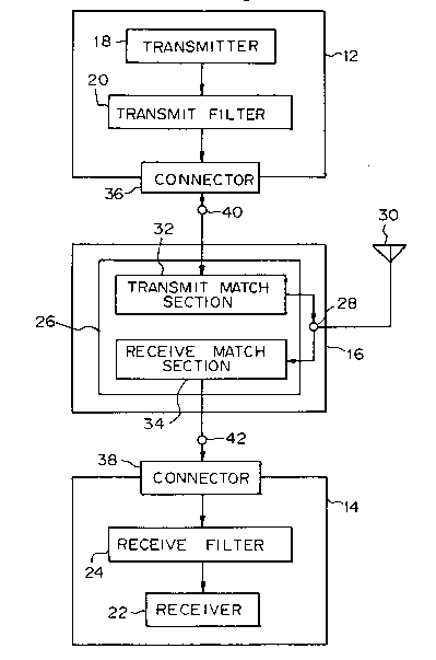
Fig. 2 is a block diagram schematically showing
electric circuitry of the duplexer shown in Fig. 1.
DESCRIPTION OF THE PREFERRED EMBODIMENT
Referring to Fig. 1 of the drawings, a duplexer for
radio equipment embodying the present invention is shown and
generally designated by the reference numeral 10. As shown, the
duplexer 10 is generally made up of a transmission circuit board
12, a reception circuit board 14, and a connection circuit
board 16 which are physically independent of one another. The
connection circuit board 16 connects the transmission and
reception circuit boards 12 and 14 generally in a U
8050 ~
--4--
configuration. The transmission circuit board 12 has a
transmitter section 18 and a transmit filter 20 and outputs a
high frequency signal to be transmitted. The transmit filter 20
filters out noise from the the output signal of the transmitter
5 section 18 so as to pass only the predetermined high frequency
signal.
The reception circuit board 14 has a receiver section 22 and
a receive filter 24. The receiver section 22 receives a high
frequency signal from a remote station, not shown, while the
10 receive filter 24 passes only the predetermined high frequency
signal to the receiver section 22 by removing noise from the
received signal. The reception circuit board 14 has substantially
the same dimensions as the transmission circuit board 12. The
transmission and reception circuit boards 12 and 14 are
15 arranged back-to-back and in parallel to each other.
As shown in Fig. 2, the connection circuit board 16 has a
matching circuit 26 which is interconnected to an antenna 30 via
an antenna terminal 28. The matching circuit 26 is constituted
by a transmit matching section 32 and a receive matching section
20 34. The transmit matching section 32 matches the output
impedance of transmit filter 20 and the impedance of antenna 30
and receive side (14~ as viewed from the antenna terminal 28.
In other words, a combination of the transmit filter 20 and
transmit matching section 32 serves to pass the transmit high
25 frequency signal from the transmit section 18 and to block the
2018~50
--5--
other signals. As shown in Fig. 1, the transmit matching
section 32 is implemented as a line of copper foil extending out
from the antenna terminal 28. The transmit matching section 32
has the same impedance as the transmit filter 20. The receive
5 matching section 34 matches the input impedance of receive filter
24 and transmit side (12) as viewed from the antenna terminal
28. In other words, a combination of the receive filter 24 and
receive matching section 34 serves to pass the receive high
frequency signal from the antenna 30 and block the other
10 signals. The receive matching section 34, like the transmit
matching section 32, is implemented as a line of copper foil
extending out from the antenna terminal 28 and has the same
impedance as the receive filter 24. The connection circuit board
16 is affixed at its back to the ad joining ends of the parallel
15 transmission and reception circuit boards 12 and 14, thereby
supporting the two boards 12 and 14 generally in a U
configuration.
Connectors 36 and 38 adapted for high frequency electrically
interconnect respectively the transmission circuit board 12 and
20 the reception circuit board 14 to the connection circuit board 16.
Specifically, the connector 36 sets up electrical connection of the
output side of the transmit filter 20 to the transmit end 40 of the
transmit matching section 32, while the connector 38 sets up
electrical connection of the input side of the receive filter 24 to
25 the receive end 42 of the receive matching section 34.
In operation, to transmit a signal to a remote station, the
transmitter section 18 of the transmission circuit board 12
produces a predetermined high frequency signal. The high
frequency signal is routed through the transmit filter 20,
connector 36 and transmit end 40 to the transmit matching
section 32. The output of the matching section 32 is fed to the
antenna 30 via the antenna terminal 28 and thereby radiated as
a high frequency signal wave. A high frequency signal wave
from a remote station comes in through the antenna 30 and is
applied to the receive matching circuit 34 via the antenna
terminal 28. The output of the receive matching circuit 34 is
routed through the receive end 42 and connector 38 to the
receive filter 24. The filtered signal from the receive filter 24 is
fed to the receiver section 22.
Of course, the generally U-shaped configuration of the
assembly of the three physically separate circuit boards, 12, 14
and 16 shown and described is only illustrative and may be
suitably changed or modified by taking account of the positions
of the connectors 36 and 38 as well as other conditions.
In summary, it will be seen that the present invention
provides a duplexer having various unprecedented advantages,
as enumerated below.
(1) Various components of a duplexer such as a transmitter
section, receiver section, transmit filter, receive filter and
25 matching circuit are mounted with improved efficiency. This is
2018050
--7--
especially desirable for those radio equipment which need
extremely dense arrangements, e. g. portable radio equipment.
(2 ) Since transmission, reception and connection circuit
boards are physically independent of each other, the
5 characteristics of the transmitter section and those of the
receiver section can be examined independently of each other.
This will facilitate maintenance when an error occurs in the
equipment.
(3 ) The transmitter section, receiver section and matching
10 circuit can be designed independently of one another and,
therefore, the designing time is reduced.
Various modifications will become possible for those skilled
in the art after receiving the teachings of the present disclosure
without departing from the scope thereof.