Note: Descriptions are shown in the official language in which they were submitted.
20 ~ 807 1
-- B09-87-012
CHROMATIC AND MISALIGNMENT COMPENSATION
IN A MULTIPLE BEAM LASER SCANNING SYSTEM
This invention relates to multiple beam laser scanning
systems and more particularly to electronic compensation
for picture element (pel) placement errors caused by
mechanical misalignment and wavelength (chromatic)
variations.
BACKGROUND OF THE INVENTION
Multiple beam lasing systems can be used in a variety of
applications, one of which is in a printing system where
rotating polygonal mirrors are used to scan the light
beams across a photoreceptive surface. The use of
multiple laser beams in a printing system provides the
capability of producing more than one line of information
at a time, thus enabling high pel resolution, for
example, 480 pels per inch or higher while keeping
practical speeds for the rotating polygonal mirror.
Multiple beam devices provide other capabilities as well;
that is, the multiple beams can be used to alter the
shape of the effective writing spot by modulating the
spots within the spot group or they can be used to
modulate the amount of light provided at each pel
position.
While the use of multiple beam lasing systems have
significant advantages over a single beam lasing system,
multiple beam systems employing discrete laser sources or
employing laser array chips require precise mechanical
alignment to assure that a print position (pel location)
is properly located from line to line, that is, that a
pel written by one laser is properly aligned with a pel
written by another laser. Multiple beam systems which
employ laser arrays require that the lasing diodes be
placed on the chip to close tolerance, nevertheless,
there can be some physical misplacement of the
semiconductor laser diodes within the chip making it
desirable to provide a system which can utilize laser
arrays with some laser spot variation. Additionally,
Z~18~71
- B09-87-012 2
laser array chips are typically mounted in a tilted
fashion to provide correct beam alignment in the non-scan
direction. However, the tilt creates an offset from beam
to beam in the scan direction creating pel placement
problems. As used herein, the term mechanical
misalignment includes: 1) physical variation in the
placement of lasing spots on a laser array chip; 2)
mechanical misalignment of the laser array chip or of
discrete lasing sources within a machine; and 3) the
offset produced by tilting a laser array.
Still another problem with multiple beam lasing systems
is wavelength variation from laser beam to laser beam.
In laser arrays, wavelength variation is often within a
few nanometers, but can be significant enough to create
pel placement problems. In addition, it is desirable to
utilize laser arrays with a wider range of wavelength
variation in order to produce low cost systems. Such
considerations are also true of multiple beam systems
utilizing discrete laser sources. In any event, even if
lasing sources are carefully matched, temperature and age
can create dynamic wavelength variation which can destroy
the accuracy of the system. It should be noted, that
laser beam position is typically amplified through
printhead optics, such that a small misalignment at the
laser chip or a small wavelength variation can result in
a much larger error at the focal plane.
Electronic correction schemes in the prior art have been
designed to achieve multiple pel corrections for
misalignments due to a necessary tilting of a laser
array. Additionally, some of these electronic schemes
provide sub-pel accuracy. Such systems require
nanosecond capability when high resolution systems are
contemplated, that is, 480 pels per inch or higher.
Clock frequencies of 500 x 106 Hz are required to resolve
to two nanoseconds. Such a clock and the high speed
logic utilizing such resolution are expensive.
It is an object of this invention to provide an
electronic correction scheme for use with a multiple beam
2~8~1
-- B09-87-012 3
scanning laser system to provide correction for
mechanical misalignment errors.
It is also an object of this invention to provide an
electronic correction scheme for use with a multiple beam
scanning laser system to provide correction for chromatic
errors.
It is another object of this invention to quantify
misalignment errors separately from chromatic errors in
order that the two types of errors can be separately
compensated.
It is an object of this invention to provide a multiple
beam printhead such that proper chromatic operation is
achieved while utilizing lasing sources of significantly
different wavelength.
It is still another object of this invention to provide
an electronic correction scheme utilizing relatively low
clock frequencies, but providing correction resolution to
within one or two nanoseconds.
It is still another object of this invention to provide a
chromatic correction scheme which adjusts the clock
across the entire scan.
It is still another object of this invention to provide
an electronic correction scheme which is adaptive to
dynamic variations in wavelength which may occur due to
temperature or age.
SUMMARY OF THE INVENTION
This invention relates to electronic correction for
chromatic aberrations and mechanical misalignment
problems within a multiple beam laser printhead by
separating the chromatic aberrations from the
misalignment problems and providing separate correction
techniques for each type of error. A constant adjustment
is made to each pel position in a given scan line to
2~1807'1
~ B09-87-012 4
correct for mechanical misalignment while delays are
inserted into the scan line at intervals to correct for
chromatic aberrations. Sub-pel correction is achieved
for both mechanical misalignment and chromatic
aberrations through the use of tapped delay lines.
The invention is advantageously practiced by selecting
one of the laser beams as a reference beam and aligning
pels produced by the other beams to the pels produced by
the reference beam. To do that, the mechanical
misalignment must be corrected; a start reference pulse
is produced by the reference beam followed by a reference
beam start of scan (SOS) pulse. Similarly, the reference
beam is used to generate an end reference pulse and an
end of scan (EOS) pulse. The time period Tnoml is
measured between the start reference pulse and the SOS
pulse and the time period Tnom2 is measured between the
end reference pulse and the EOS pulse. Next, a
non-reference laser is energized to produce a second SOS
pulse and a second EOS pulse. The time period Tl is
measured between the start reference pulse and the second
SOS pulse and the time period T2 is measured between the
end reference pulse and the second EOS pulse.
Thereafter, the mechanical offset of the non-reference
beam is calculated according to the relationship:
( Tnom2 - T2 ) + ( Tnoml - Tl )
The start of scan for the non-reference beam is then
altered to compensate for the offset and thereby produce
aligned pels at the center of process.
Chromatic aberrations can cause misalignment of pels
during the scan even though the center of process pels
are aligned. Therefore, the next step is to measure the
displacement time between the reference beam SOS signal
and the non-reference beam SOS signal. An appropriate
delay can then be inserted to align the two SOS signals
and additional delays can be inserted at selected
2~18~71
- B09-87-012 5
intervals throughout the non-reference scan to maintain
pel placement alignment at a desired tolerance.
BRIEF DESCRIPTION OF THE DRAWING
The above mentioned objects and other features and
objects of this invention, and the manner of attaining
them will become more apparent and the invention itself
will best be understood by reference to the following
description of embodiments of the invention taken in
conjunction with the accompanying drawing, the
description of which follows.
FIG. 1 is a diagrammatic representation of an
electrophotographic machine.
FIG. 2 shows a laser array optical system for use in the
machine of FIG. 1.
FIG. 3 shows a discrete lasing source optical system for
use in the machine of FIG. 1.
FIG. 4 is a diagrammatic representation showing a laser
array tilted to produce proper pel alignment in the
process direction, but thereby creating improper pel
alignment in the scan direction unless corrected.
Corrected pel placement is shown.
FIG. 5 shows the effect of mechanical offset and
chromatic aberrations from scan line to scan line.
FIG. 6 is an illustration of pel placement errors for a
scan line exhibiting chromatic aberration.
FIG. 7 illustrates signals needed to separate mechanical
misalignment errors from chromatic aberrations.
FIGS. 8 and 9 illustrate the circuits used for correcting
mechanical misalignment.
20180~1
- BO9-87-012 6
FIGS. lO and 11 illustrate the circuits used for
correcting chromatic aberrations.
DETAILED DESCRIPTION
The application of this invention can be illustrated
within the framework of electrophotographic machines
wherein prints are produced by creating an image of the
subject on a photoreceptive surface, developing the
image, and then fusing the image to paper or other print
receiving material. In most electrophotographic machines
the electrophotographic process is of the transfer type
where photoreceptive material is placed around a rotating
drum or arranged as a belt to be driven by a system of
rollers. In the typical transfer process, photoreceptive
material is passed under a stationary charge generating
station to place a relatively uniform electrostatic
charge, usually several hundred volts, across the
entirety of the photoreceptive surface. Next, the
photoreceptor is moved to an imaging station where it
receives light rays from a light generating source which
will discharge the photoreceptor to relatively low levels
when the light source is fully powered, while the
photoreceptor will continue to carry high voltage levels
when the light source is turned off, or when it is
powered at intermediate levels or for a relatively short
duration. In that manner, the photoreceptive material is
caused to bear a charge pattern which corresponds to the
printing, shading, etc., which is desired to be printed
on the receiving material.
Light generating sources in an electrophotographic
printer are frequently comprised of lasing means in which
the beam is modulated by a character generator to control
the power or the length of time that a beam exposes the
photoconductor in a particular pel area. In a multiple
beam lasing system, character generators may modulate
more than one beam at a time, so that more than one line
of pels may be written at a time.
2~18~71
- B09-87-012 7
After producing an image on the photoreceptor, the image
is moved to a developing station in the machine where
developing material called toner is placed on the image.
This material is usually in the form of a powder which
carries a charge designed to cause the powder to deposit
on selected areas of the photoreceptor.
The developed image is moved from the developer to a
transfer station where the copy receiving material,
usually paper, is juxtaposed to the developed image and a
charge is placed on the backside of the paper so that
when it is stripped from the photoreceptor the toner
material is held on the paper and removed from the
photoreceptor.
The remaining process steps are for permanently bonding
toner material to the copy paper and cleaning residual
toner left on the photoreceptor so that it can be reused.
FIG. 1 shows a typical electrophotographic machine such
as would be used to implement this invention.
Photoreceptive material lO is placed on the surface of a
drum 11 which is driven by motive means, not shown, to
rotate in the direction A. A charge generator 12 places
a uniform charge of several hundred volts across the
surface of the photoreceptor at charging station 12 .
The charged photoreceptor is mounted in a dark enclosure,
not shown, and rotates to a printhead 13 which is
comprised of a light generating source, such as a
multiple beam laser generator. The light source
selectively exposes the charged photoreceptor at imaging
station 13 to discharge it in areas which are desired to
be developed (Discharged Area Development, DAD process),
or discharge it in areas which are to remain free of
toner (Charged Area Development, CAD process).
For a DAD process, the discharged areas of the
photoreceptor are developed at developing station 14 by
developer apparatus 14 which applies toner so that the
photoreceptor carries a visually perceptible image of the
data. In a CAD process, the charged areas are developed.
2~18~71
- B09-87-012 8
In either case, the developed image rotates to transfer
station 15 where print paper, moving in the direction B,
is juxtaposed with the surface of the photoreceptor. A
charge opposite in polarity to the charge on the toner is
placed on the backside of the print paper by transfer
charge generator 15 such that when the paper is stripped
from the surface of the photoreceptor, toner will be
attracted to the paper and leave the surface of
photoreceptor 10. Any remaining residual toner is
cleaned from the photoreceptor at cleaning station 16 by
cleaning apparatus 16.
The selective application of light rays to the
photoreceptor 10, at imaging station 13, is accomplished
through printhead modulator means 17. For a
semiconductor laser diode, the printhead modulator is
comprised of a power supply, which will either turn the
light source on for longer or shorter periods of time to
accomplish varying degrees of photoreceptor discharge in
accordance with the pattern data, or it will turn the
light generating source on to a greater or lesser
illumination intensity in accordance with that data. In
any event, modulation will occur in accordance with that
data contained in memory 19. That data is sent to a
raster buffer 18 and on to the printhead modulator 17.
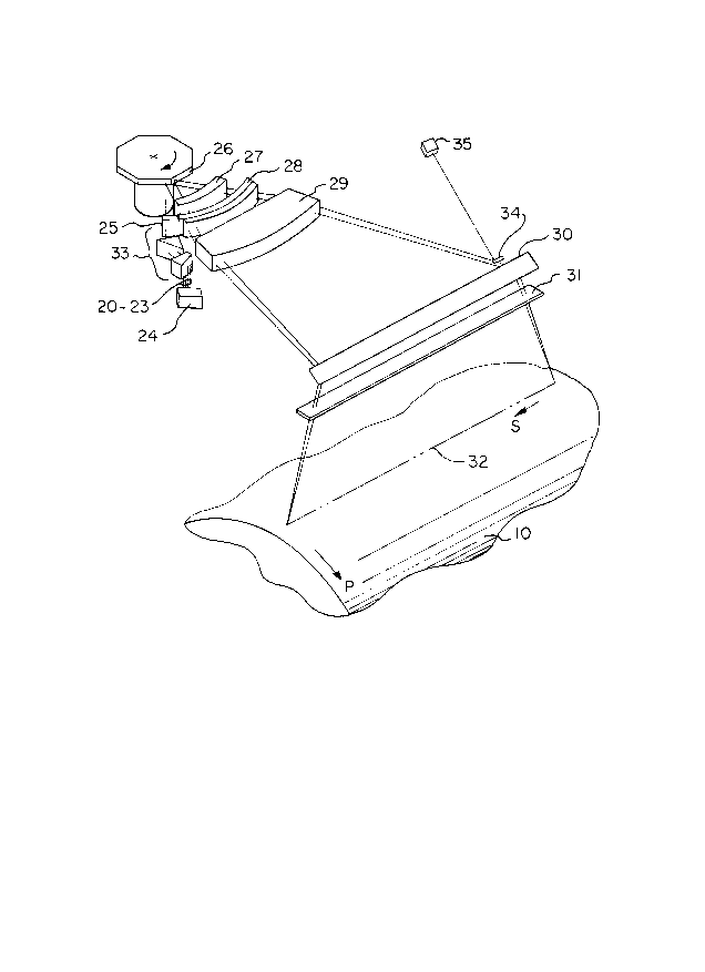
FIGS. 2 and 3 show optical scanning systems which can be
used in the machine of FIG. 1. Either of these can be
utilized in printhead 13. In the multiple beam system
illustrated in EIG. 2, four (4) nearly coaxial laser
beams 20-23 are shown emanating from a multiple beam
laser array module 24. FIG. 3 shows a laser beam module
24 which has four (4) discrete laser chips 5-8 whose
laser beams 20-23 are passed through beam combining
optics 9. In either system, the four (4) laser beams
20-23 are passed through a cylindrical lens 25 for
focusing each of the beams onto the facets 26 of a
rotating polygonal mirror. The beams are reflected from
the rotating mirror through a negative spherical lens
group 27, anamorphic lens group 28, and a positive
spherical lens group 29, and onto the surface of
2~18~)71
B09-87-012 9
photoreceptor 10. FIGS. 2 and 3 show a fold mirror 30,
an exit window 31, the length 32 of the scan across
photoreceptor 10, and beam expanding or collimating
optics 33. A reflective surface 34 is provided to
reflect light from each laser beam to photodetector 35 in
order to derive start of scan (SOS) signals. A similar
arrangement can be used for generating end of scan (EOS)
signals or a reflective surface can direct the end of
scan light beam back to detector 35 so that the same
detector can be used for generating both SOS and EOS
signals.
FIG. 4 is an illustration of the need to tilt laser array
module 24 in order to provide proper pel placement in the
process direction P. At a resolution of 480 pels per
inch, pels must be placed at 480th of an inch intervals
(b dimension in FIG. 4). The lasing spots on the array
24 would require a similar close spacing in order to
locate the laser array 24 parallel to the axis P of the
process direction. However, it is not practical to
manufacture laser arrays to such tight tolerances.
Therefore, array 24 is tilted, as shown in FIG. 4, at an
angle such that the lasing spots can be separated a
distance a greater than b and still produce pels which
are properly spaced a distance b. In so doing, the
lasing spots are offset a distance c in the scan
direction S. Therefore, it is necessary in laser array
systems to electronically offset the start of printing in
the scan direction between laser beams in order to mate
pel locations properly.
While discrete laser sources do not have the tilt induced
problem described above with respect to laser arrays, it
is difficult to locate the four discrete lasing sources
5-8 shown in FIG. 3 with such accuracy that no mechanical
misalignment is present. It is therefore, desirable to
electronically correct for mechanical misalignment errors
in discrete laser source printheads in order to avoid
expensive laser chip placement systems and/or dynamically
adjustable chip placement systems in such printheads.
2018~I
~~ B09-87-012 10
FIG. 5 illustrates the effect of mechanical and chromatic
aberrations in the production of scan lines. If scan
line 40 (which may be produced by laser beam 20, FIG. 4)
is chosen as the reference scan line, scan line 41 ~which
may be produced by laser beam 21) exhibits a reduced
length relative to scan line 40, but is symmetrical
around the center 44 of the scan line 40. Scan line 42
(which may be produced by laser- beam 22) exhibits a
reduced magnitude relative to scan line 40 and in
addition is not symmetrical around the center 44 of the
reference scan line 40. This scan line trace shows that
scan line 41 exhibits no mechanical misalignment, but is
reduced in size due to variations in wavelength between
scan line 41 and the reference scan line 40. Differences
in wavelength create differences in the amount each beam
is refracted as it passes through the lens system shown
in FIGS. 2 and 3, since the index of refraction of glass
changes with wavelength. As a result, there is a lateral
separation between beam 40 and 41 in the scan direction
at the image plane. Shown in FIG. 5, if the center pels
of each beam line up properly as they do between scan
lines 40 and 41, there is a different starting pel
position and a different ending pel position for lines
printed by the beams. If the wavelength difference is
great enough, a serious print quality defect results.
In FIG. 5, scan line 42 is produced by a lasing source of
the same wavelength as scan line 41, that is, the length
of scan line 42 is equal to the length of scan line 41,
however, the two beams do not line up with one another
since scan line 42 has been produced by a lasing source
which is mechanically out of alignment with the reference
scan line 40 and with scan line 41. As a result of the
mechanical misalignment, all of the pels in scan line 42
are displaced a constant amount in one direction.
FIG. 5 illustrates that in order to correct the chromatic
aberration problem of scan line 41, the scan line must be
extended by a time period delta t at the start of scan
and similarly expanded by delta t at the end of scan.
FIG. 5 illustrates that scan line 42 must be expanded by
2018~1
~- B09-87-012 11
the time delta t minus the offset at the start of scan,
and extended by delta t plus the mechanical offset at the
end of scan.
FIG. 6 illustrates pel placement error across the scan
from start of scan to end of scan for scan line 41. FIG.
6 is an idealized depiction showing a linear change in
pel placement across the entire scan, but is suitable for
explaining the principles of the invention. In
actuality, the pel placement error may be greater from
pel to pel toward the edges of the scan than at the
center of the scan. In addition, depending upon the
optics used in the printhead, the pel placement error may
not be symmetrical around the center of the scan, but may
vary widely over the scan. Whatever the situation, it
can be characterized at manufacture and the principles of
this invention can be applied. The simplest case, which
is a linear pel placement error, as shown in FIG. 6, will
be used to explain the invention.
FIG. 7 shows signals produced from the start of scan
detector 35, shown in FIGS. 2 and 3, for use in
separating the mechanical misalignment error from the
chromatic aberration. The technique requires that
detector 35 be either a dual detector or a detector with
a mask separating the light receiving area into two
active regions. The technique also requires a clock that
is gated, that is initiated, by the start of scan (SOS)
signal. This clock can be the system pel clock as
illustrated in this embodiment, but it can be a different
precision clock if desired. In this embodiment, one
laser is assigned to be the reference laser, for example,
the laser which produces scan line 40 in FIG. 5. This
laser is powered on to generate a start reference signal
45 and a start of scan (SOS) signal 46. The time period,
Tnoml is measured between these two pulses. Similarly,
the reference laser is utilized to generate an end
reference signal 47 and an end of scan (EOS) signal 48.
The time period, Tnom2 is measured between these two
pulses. Next, a non-reference laser is enabled to
generate start of scan and end of scan pulses. For
2~18~1
B09-87-012 12
example, laser 42 in FIG. 5, might be enabled to generate
start of scan pulse 49 and end of scan pulse 50. The
time period T1 between reference pulse 45 and
non-reference start of scan pulse 46 is measured,
together with time T2 between end reference pulse 47 and
non-reference end of scan pulse 50. With these
measurements the mechanical offset is then calculated by
the following algorithm.
( Tnom2 - T2 ) + ( Tnoml - Tl )
Note that adding the offset at the start of scan and the
offset at the end of scan will result in a total offset
of zero if the two offsets are equal. In such case,
there is no mechanical offset.
FIGS. 8 and 9 show a preferred technique for correcting
the mechanical offset found through the use of the
signals generated in FIG. 7. The technique shown
measures the difference between the signals 45 and 49,
and the difference between the signals 47 and 50 to a
sub-pel level. FIG. 8 illustrates that a gated clock is
gated on by the start reference pulse 45, and that the
pulse 49 to be measured occurs at some point during the
seventh clock cycle. Instead of using an expensive high
frequency clock to measure the difference between clock
pulses 7 and 8 to a sub-pel basis, the circuit of FIG. 9
is used, employing a tapped delay line 54 to resolve the
time period at which pulse 49 rises during clock pulse 7.
The circuit of FIG. 8 first determines during which cycle
of the clock that the event occurs. In this case pulse
49 occurs during the seventh clock cycle. To do that, a
signal is shifted through a shift register 70 on each
clock cycle. The outputs of the shift register are
connected to a multiplexer 51. The control line 52 of
the multiplexer determines which cycle the event is
tested for, and consequently, the change in serial
register output is sensed as occurring during clock cycle
2nls~7l
B09-87-012 13
7. The output 53 of multiplexer 51 is connected to a
tapped delay line 54. The delay interval between
successive taps determines resolution of the final
measurement. Consequently, if the resolution of tapped
delay line 54 is 2 nanoseconds, then that is the
resolution of the final measurement. As a practical
note, the total delay of all the taps in delay line 54
should exceed one clock time so that each successive test
at a given clock interval overlaps with the previous and
succeeding interval. In that manner, should pulse 47
occur near the change of state of the gated clock, it can
still be resolved to the sub-pel accuracy of the delay
line.
To obtain sub-pel resolution, the selected event, that is
pulse 49, initiates a succession of high resolution
timing pulses A-N during clock cycle 7, as shown in FIG.
10. These pulses are each of 2 nanosecond duration and
are generated through the delay line 54. The event,
pulse 49, sets a pattern into the latches 55-57 from
which the timing information is determined. For example,
if the rise of pulse 49 occurs between tap A and tap B,
latch 55 will possess a different setting than taps B-N.
The maximum relative resolution is not limited by the
performance of the latches since the set up time for the
latches is constant from one measurement to another.
Therefore, the set-up time falls out of the time
measurement when the difference between two measurements
is of interest. This technique, therefore, determines
the rise of pulse 49 relative to pulse 45 within 2
nanoseconds.
What has been described above is the measurement of time
interval Tl. In a similar manner, time interval T2 is
ascertained, together with the time intervals Tnoml and
Tnom2. With all of the measurements needed to implement
the calculation of mechanical offset, a controller, not
shown, performs the calculation and adjusts pel location
by providing a proper delay into the timing of scan line
42, FIG. 5, so as to move that scan line in such a manner
that the center of scan line 42 is along the center of
2nls~7~
- B09-87-012 14
reference line 40. By so doing, scan line 42 will take a
position exactly like that of scan line 41. With the
correction of mechanical offsets in all of the scan
lines, it is then necessary to correct for the chromatic
aberrations exhibited by scan lines 41 and 42, to expand
those scan lines to equal the length of reference scan
line 40.
In order to provide chromatic compensation for scan lines
41 and 42, they must be expanded to equal scan line 40.
To do that, the mechanical misalignment between scans is
corrected as above, and then the relative displacement of
the start of scan signals to the reference beam SOS
signal is measured. This displacement results from
wavelength differences and is equal to:
Chromatic Error (Tnom2 - T2) - (Tnom1 - T1)
At Start of Scan
Typically, variations in pel placement due to wavelength
differences are less than one pel. To provide
compensation in the case of a linear pel placement error
such as explained with reference to FIG. 6, a periodic
delay is placed in the printing of pels throughout the
scan. That is to say, if the total scan line is 7,000
pels long, it is 3,500 pels from the start of print to
the center of print, where all center pels are aligned.
If the total error is measured as 1/2 pel between the
start of scan signals of reference scan line 40 and the
scan line 41, and if the requirement is to produce pels
which are never more than 1/lOth pel out of alignment, a
minimum of five corrections are needed over the 3,500 pel
length. Therefore, a periodic correction of 1/lOth pel
is inserted every 700 pels during production of the scan
line 41.
FIG. 11 illustrates a circuit to perform the chromatic
aberration correction. The pel clock is applied to a
multiple tapped delay line 60. The amount of delay
between each successive tap determines the resolution of
%~18071
- B09-87-012 15
the correction. The various taps A-N are applied to the
input of digital multiplexer 61. A control line 62 is
provided to select each phase of the pel clock and
thereby ascertain the tap at which the change of state
occurs in the same fashion described above with reference
to FIGS. 8 and 9. A programmable counter 64 and phase
select logic 63 can be utilized in the selection process.
In the example described above, if tap F represents the
center of print and tap A represents the start of print
pel, the delay in output from tap A will equal .5 pel
from the center of print to a resolution of 2
nanoseconds. Tap B will represent a delay of .4 pel from
the center of print and will be utilized to provide the
delay 700 pels into the scan. Tap C represents a delay
of .3 pel from the center of scan and will be timed to
occur 1,400 pels into the scan. In a similar manner,
corrections of l/lOth pel are placed into the line at
2,100 pels and at 2,800 pels. On the trailing side of
the center of print, similar corrections are made to the
pel clock.
In the case where pel placement is not symmetric around
the center of print, a table can provide the pel count at
which delays are to be implemented. Note also that scan
lines can be magnified with respect to the reference
creating a need for line contraction rather than
expansion. The technique is the same except that the pel
clock pulse is moved incrementally forward in accordance
with the selected tap.
As mentioned previously, the wavelength of a laser can
vary with time and temperature, therefore, the tap which
best corrects for the relative error can change over
time. With reference to FIG. 7, this means that there
can be a drift in the start reference pulse 45 and there
can be a drift in the position of pulse 49 representing
the start of scan pulse for scan line 42. As a result,
the corrections needed can change with time and
temperature. Therefore, the circuits of FIGS. 8 and 11
are enabled to select the tap to be used in accordance
2~18~)7~
B09-87-012 16
with the detection of the reference start of scan and the
start of scan for the non-reference laser periodically
throughout machine use. In that manner, the correction
is a dynamic correction which adapts to changes as the
pulse positions shift.
While the invention has been shown and described with
reference to a preferred embodiment, it will be
understood that changes in the form and details of the
invention may be made therein without departing from the
spirit and scope of the invention. For example, a
grating system could be used for generating reference
pulses and all scan lines can be adjusted accordingly.