Note: Descriptions are shown in the official language in which they were submitted.
33~5 :
...
The present inventlon relates to a multiplexed
slgnal transmitter which frec~ency-multlplexes a tele- ;~
vlsion signal, compatible wlt:h the exlsting televislon
system, with a televlsion sis~nal of a high-definitlon
system, and transmits the multlplexed signal, and a
multiplexed signal recelver which receives the multi-
plexed signal.
Recently, researches for and developments on a
high-definition lmage become promlnent in the televlsion
broadcasting. In this high-deflnition system, a televi-
sion signal of the exlsting system as a maln signal ls
frequency-multiplexed wlth a televlslon signal of a
high-definition system as a helper signal in order to
realize compatibility with the existing system; the
helper slgnal includes a hlgh-frequency component of a
luminance signal or a signal or lnformation correspond-
ing to the side portion of a wide-aspect system. There
are two frequency-multiplexing systems of the above
type: one ls dlsclosed in T. ~ukinuke et al., ~Extended
Definitlon TV Fully Compatlble Wlth Exlstlng Standards"
IEEE TRANSACTIONS COMMUNICATIONS, VOL. NO. 8, AUGUST
1984 (hereinafter referred to as Publication 1) and the
other ls disclosed ln M.A. Isnardl et al. "Encodlng for
Compatibllity and Recoverabllity in the ACTV System"
IEEE TRANSACTIONS BROADCASTING VOL. BC-33 NO.4, DECEMBER
1987" (hereinafter referred to as Publication 2).
The helper slgnal for provldlng high definition of
; .,
2~)18395
.
the main slgnal does not contribute to image reproduc-
tion in the existlng television receiver, and it is
treated with a noise signal 1;o the main signal. This
would raise a problem of interference of the helper
slgnal with the main slgnal. The helper signal is
effectively used only ln a televlsion recelver of the -;
hlgh-definition system.
To eliminate the influence requlres reduction in
multiplexed level of the helper signal.
Reduclng the multiplexed level of the helper
signal, however, reduces the signal-to-nolse (S/N) ratlo
so that the helper signal cannot be accurately repro-
duced in thP high-definition television receiver.
Since the helper signal for the high-definition
eystem is a high-frequency signal, the averaged power of
the helper signal is considered comparatlvely lower than
the averaged power of the main signal in vlew of the
general property of the televislon signal. In this
case, therefore, the interference of the helper signal
with the main signal appears insignificant. However,
this actually raises a problem of increasing the peak
value of the main slgnal at the edge portion of an
image. As the edge portion of an image corresponds to a
high-frequency signal, further multiplexing this signal
wlth a helper slgnal (hlgh-frequency slgnal) would cause ;
the multlplexed signal to exceed a transmittable level.
As a result, a reproduction signal of the edge portion
r" ~
20il3395
of the image on the receiver slde becomes inaccurate.
In order to solve thls shortcoming, the system dis-
closed in the aforementloned Publication 2 employs a
method of transmittlng a helper signal in non-linearly
compressed on the sender side and non-linearly expanding
this signal for reproduction on the recelver slde.
This method can reduce the interference of the
helper signal with the edge portion of the main signal
without reducing the S/N ratio of the helper signal.
This method, however, would raise the following two
problems.
~ 1) First, the reproduced output of the helper
signal has waveform distortion. In a non-linear com-
pressing process, a harmonic component is generated.
In transmltting a helper signal frequency-multlplexed
with a maln slgnal, on the other hand, the transmlssion
band of the helper signal ls generally set to the same
band as the spectrum band of the helper slgnal prlor to ~ -
the compression in order to lmprove the efficlency of
utillzing the transmission band. In this case,
therefore, the harmonic component generated in the non~
linear compresslng process on the sender side would not - ~ -
be transmitted to the receiver side. Consequently, `
the helper signal acquired by the non-linear expanding
process on the receiver side would have waveform
distortion.
(2) The second problem is to cause visually very
~;: . ., ' '
~ .
2~)~83~S
unnatural deterioration of the quality of an lmage. In
executing digital processing of the helper slgnal to be
transmltted as an analog slgnal on the receiver slde, an
8-bit circult ls often used as an analog-to-digltal
(A/D) converter. This is because that using a 10-blt
circuit significantly raises the cost for the overall
circuit. Although the 8-blt circuit has a resolution of
256 grad~tions, it cannot ensure 10 to 20 gradations for
a helper signal because the peak value of the helper
slgnal should be compressed to 1/10 or less in order to
elimlnate the interference of the helper signal with the
main signal. Such reduction in resolution not only
increases quantized noise but also provides a vlsually
very unnatural image. In the above example, parti-
cularly, the reduced resolution would be further empha-
sized ln the non-linear expanding process carrled out on
the receiver side, thus making unnaturalness of the
reproduced lmage more prominent.
As described above, in the prlor art apparatuses
which frequency-multiplex a helper signal for high -~
definition, having a correlation with a main signal, ;~
with this main signal and transmits the multiplexed ;
signal, although it is possible to eliminate the influ-
ence of the helper signal with the edge portion of the
main signal, the helper signal cannot be accurately
reproduced. The mentloned correlation is such that when
the level o* the main signal is high, the level of the
2~)~839S
,,
helper slgnal is hlgh, and when the level of the former
signal ls low, the level of the latter signal ls also
l~w. . ~.~
Accordlngly, lt ls an ob~ect of the present inven~
tlon to provide a multiplexed signal transmitter and a
multiplexed signal recelver, which can ellminate the
lnfluence of a helper signal wlth the edge portion of
a main slgnal and accurately reproduco the helper
signa~
To achieve thls ob~ect, the multiplexed signal
transmitter of this invention comprlses energy detector
for detectlng energy of a plurality of pixels of a main :-
signal as a television signal; level controller for con~
: trolllng the level of a helper signal having a correla- .. :
tion with the main signal, based on a detection output
of the energy detector; and frequency-multlplexer for
: frequency-multiplexing the helper slgnal having its -
level controlled by the level controller, wlth the main - --
signal. ;~
It is another ob~ect of this lnvention to provide a
multiplexed signal receiver which receives a multiplexed
signal that is acquired by frequency-multiplexing a
helper signal having a correlation with a main signal
:,
as a telev1sion signal, with this maln slgnal. .-
To achieve the 3econd ob~ect, the multiplexed
signal receiver of this invention comprises a receiver
for receiving a multiplexed signal acquired by ~
~ 2~ 395
-- 6 --
frequency-multiplexlng a helper signal having a correla-
tion wlth a main signal as a televlsion signal with the
main signal, the helper signal having a level controlled
on the basis of an output resultin~ from detectlon of
energy of a plurality of pix21s of the main slgnal;
freguency-multiplexed slgnal separator for frequency-
separatlng the multiplexed slgnal into the main slgnal
and the helper signal; energy detector for detectlng
energy of a plurality of pixels of the main slgnal sepa-
rated by the frequency-multiplexed signal separator; and
level controller for controlling the level of the helper
signal, separated by the frequency-multiplexed slgnal
separator, in a characteristic opposite to that obtalned
on a sender side, based on a detectlon output of the
energy detector.
With the above arrangements, since the main signal -
and helper signal have a correlation, it is possible to
ensure a correlation between an output resulting from
detection of the energy of the main slgnal and the
helper signal. It is therefore posslble to suppress the
level of the helper signal at the edge portion of the
main signal where the level of the energy detection out-
put becomes large. The level suppression can reduce the
interference of the helper signal with the main signal
at its edge portion.
Further, since the detected energy is for a plural-
ity of pixe].s, unlike the main signal, the detection
2~)1839S
output does not have a wide spectrum but has only a low-
frequency component. Even if the level of the helper
slgnal ls controll~d on the basis of the energy detec- -
tion output, therefore, the spectrum of the helper sig-
nal hardly becomes wider. Thls permits transmlssion of
a level-controlled helper slgnal in the spectrum band
of the original helper signal, so that a reproduced
output of the helper signal does not have wave dlstor-
tion.
Furthermore, since the main signal is sent as it is
to the receiver side, the receiver side can acquire the
quite the same energy of the main signal as the one - ;-
obtained on the sender side. Accordingly, the original
helper signal ~an accurately be reproduced on the
receiver side without degradlng the resolution at all.
In addition, as the level control on the sender
side and that on the receiver side need to have the
opposite characteristlcs, there is a more freedom in
selecting the required control mode.
This invention can be more fully understood from
the following detailed description when taken in con-
~unction wlth the accompanying drawings, in which:
Fig. 1 is a circuit diagram illustrating the struc-
ture of the flrst embodlment of a multiplexed signal
transmitter according to the present invention;
Fig. 2 ls a circuit diagram illustrating the struc-
ture of the first embodiment of a multiplexed signal
~:018395
receiver according to the present invention;
Fig. 3 is a circuit dlagram illustrating the struc-
ture of the second embodiment of a multiplexed signal
transmitter according to the present invention;
Fig. 4 is a clrcuit dlagram lllustrating the struc-
ture of the second embodiment of a multiplexed slgnal
receiver according to the present invention;
Fig. 5 ls a circuit diagram lllustrating the struc-
ture of the third embodlment of a multiplexed signal ~ ~-
transmitter according to the present invention;
Fig. 6 ls a circuit diagram illustrating the struc~
ture of the third embodiment of a multiplexed signal
receiver according to the present inventlon;
Fig. 7 is a chart showing the band characteristic
of an input signal to the circult shown in Fig. 5;
Figs. 8A and 8B are spectrum diagrams in a spatial
frequency region given for explaining the ba~d-limiting
functlon of a 2D LPF shown in Fig. 5;
Flg. 9 is an explanatory diagram of a field signal
for explaining the output of a selector shown in
Fig. 5;
Figs. lOA and lOB are spectrum diagrams in a
spatial frequency region for the output of a vertlcal
LPF shown ln Flg. 5;
Fig. ll is a spectrum diagram along the horizontal
frequency axis of the output of a multiplier shown in
Fig. 5; ;
-,
'~, :.',.:..'.'
' ",.~. ' ;' '
~ - 2(~ 339S
Flg. 12 1~ an explanatory dlagram of the spectrum ~
along the horizontal frequency axis of the output of a - ~-
,
BPF shown in Fig. 5; ~.
Figs. 13A and 13B are explanatory diagrams of the
spectrum in a spatial frequency region for the output of
the BPF shown ln Fig. 5;
Fig. 14 is a circuit diagram illustrating a spe~
, .........
clflc structure of the 2D LPF shown in Fig. 5 ~ ~:
Fig. 15 ls a circuit diagram illustrating a spe~
cific structure of the vertlcal LPF shown in Fig. 5;
Figs. 16A and 16B are explanatory diagrams of a
field signal given for explalning the operation of the ~ -
circult shown in ~lg. 15;
Figs. 17A and 17B are explanatory diagrams of the
spectrum in a spatial frequency region for the output of
a horlzontal/vertical HPF shown in Flg. 6;
Figs. 18A and 18B are explanatory diagrams of the
spectrum in a spatlal freguency region for the output of
an adder 116 shown in Flg. 6; ~ -
Figs. l9A and l9B are explanatory diagrams of the
spectrum in a spatial frequency region for the output of
a BPF 120`shown ln Flg. 6;
Fig. 20A and 20B are explanatory dlagrams of the
spactrum in a spatial freguency region for the output of
an adder 117 shown ln Fig. 6;
Fig. 21 is a circuit diagram lllustrating another
embodiment of accumulators shown in Figs. 5 and 6;
' '.' ~ ~-
Z(~83~S
-- 10 --
Fig. 22 is a clrcult dlagram illustrating the
fourth embodiment of a multlplexed signal transmitter
according to this invention;
Fig. 23 is a circuit diagram illustratlng the
fourth embodiment of a multlplexed signal receiver
~ according to this lnvention; -~
; Fig. 24 ls a dlagram lllustrating the screen format
ln a case where a television signal of a wide aspect
system is received by a television receiver o~ the
existing NTSC system;
lg. 25 ls a diagram illustratlng the screen format
ln a case where a television signal of a wide aspect
system is recelved by a televlsion recelver of the wide
aspect system;
Figs. 26A and 26B are explanatory diagrams of the
spectrum in a spatial frequency region for the output of
a vertical LPF 162 shown in Fig. 22:
Figs. 27A and 27B are explanatory dlagrams of the
spectrum in a spatial frequency region for the output of
a subtracter 163 shown in Fig. 22;
Fig. 28 ls a c1rcuit diagram illustrating a ~--
specific structure of the vertical LPF 162 shown in
Fig. 22; -
Fig. 29 is a diagram illustrating the screen format
for explaining the operation of a tlme-compressor shown
in Fig. 22; -
Fig. 30 is a diagram illustrating a speclfic - ~
~''.' - :'
~:011~139S ~
, ',
structure of the time-compre~sor shown ln Fig. 22;
Fig. 31 is an explanatory diagram of a tlme-
compressed field signal given for explaining the opera~
tlon of the time-compressor shown in Fig. 30; ~ ;
Fig. 32 ls a diagram presented for explaining the
operation of a line interpolation clrcuik shown in
Fig. 22; and
Fig. 33 ls an explanatory diagram of the time axis
given for explaining the operation of a delay controller
shown in Fig. 23.
Preferred embodiments of thls invention wlll now be
descrlbed ln detail referring to the accompanying
drawings.
Fig. 1 is a circuit diagram lllustrating the struc-
ture of the first embodiment of a multiplexed signal
transmitter according to the present invention. Fig. 2
; is a circuit diagram illustrating the structure of the
first embodiment of a multiplexed slgnal receiver -
according to this invention. Neither Fig. 1 nor Fig. 2
shows a system for processing a chrominance signal.
To begin w1th, the multiplexed signal transmitter
shown in Fig. 1 will be described below. --~
Referring to Fig. 1, numeral 1 denotes an input ~-
terminal for a main signal Yl of a luminance signal Y,
and numeral 2 an input terminal for a helper signal Y2
of the luminance signal Y. The main signal Yl and the
helper signal Y2 have a correlation; for example, they ;~
3395
. . .
2 --
:
are a low-frequancy component and a high-frequency com-
ponent of a television slgnal, respectively. In thls
example, the maln signal Yl is a low-frequency compo-
nent transmlttable ln a band of the existing system,
while the helper signal Y2 ls a high-frequency compo-
nent exceeding this band of the exlstlng system.
The maln signal Yl input through the lnput termi-
nal l is supplied to a two-dlmenslonal ( 2D) low-pass
filter ~LPF) 11, whlch in turn sub~ects it to band-
limitatlon. Thls band-limitation is executed to provide
space ln part of a spatial frequency reglon of the main
signal Yl and put a helper signal (which will be
described later) ln thls space. The main signal Yl from
the 2D LPF ll ls supplled to an adder 16 where lt ls ~
frequency-multiplexed with a helper slgnal Y2~ acqulred ~ -
through level control. This multlplexed slgnal wlll
be transmitted by a transmittlng sectlon (not shown)
connected to an output terminal 17.
The level of the helper signal Y2' is controlled
as follows.
~ : .
The helper signal Y2 lnput through the input ter-
minal 2 is supplled to a filter 12 whlch limlts the band -
of the helper slgnal Y2 in such a way that the band of ~ -
this helper signal matches with the space in the main -~
signal Yl, in a case where the helper slgnal ls
frequency-multlplexed wlth the main slgnal. The output
from the fllter 12, Y2L2, is multiplied by a factor of ~ ;
--- 2()~L8'3~S
- 13 -
~ .
A (constant) ln a level converter 13. Thls level-
converted output is supplied to a divider 14 where it is
sub~ected to division uslng a control signal X (energy ~ ;
lnformatlon) as a divisor, ac:quired from the main signal
Yl. A helper signal Y2L3 acs~ired by thls divlslon ls
shifted to a band suitable for frequency-multiplexlng
wlth the main signal Yl by a frequency multiplexer 15.
The resultant slgnal Y2' is frequency-multiplexed with
the main signal Yl by the adder 16.
10The control signal x ls acqulred as follows.
The maln slgnal Yl from the 2D LPF 11 ls supplied
to an absolute value circuit 18 which obtains its abso-
lute value. The absolute value is accumulated for N
plxels (N being an integer equal to or greater than 2)
by an accumulator l9. The accumulated output is added
to a predetermined fixed value 3 by an adder 20. The
added result is used as the aforementioned control
signal X. The fixed value B, a ratlonal number` serves
to prevent the output of the subsequent division from
going to infinity when the accumulated output is 0.
The thus acquired control signal X is expressed by
a equation (1) below. ; ~
X = 2 Xo + B ............................. (l) ~ ;
As the helper signal Y2 is divided by this control
signal X, the helper signal ~2L3 from the divider 14 is
expressed as follows~
Y2L3 - Y2L2/X ~ L (2) ~ ~ ~
2018395 --
- 14 -
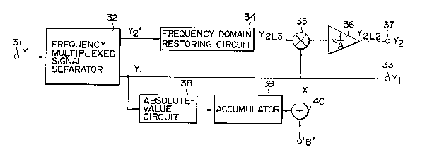
The multlplexed signal receiver shown in Flg. 2
will now be described.
Referring to Fig. 2, numleral 31 denotes an lnput
termlnal to which a multiplex~ed signal Y is input. This
multiplexed signal from the input termlnal 31 ls sepa- -
rated into a main slgnal Yl and a helper signal Y2' by a ~.
frequency-multiplexed signal separator 3~
The maln signal Yl separated by the slgnal sepa-
rator 32 i3 supplied to an lmage display section (not
shown) connected to an output termlnal 33. As the
helper slgnal Y2' has lts frequency domaln shlfted by -~
the frequency multlplexer 15 on the sender side, this
domain is restored to the original one by a frequency -
domain restorlng clrcuit 34 so that the slgnal becomes :~ :
a helper signal Y2L3. This helper slgnal Y2L3 is multi~
plled by a control slgnal x, acquired from the main sig~
nal Yl, by a multlpller 35. Thls control signal X, llke ` ~.
.. .-....
the one obtalned on the sender side, takes a value
expressed by the equation (1). Level-convertlng the ; ~;-
output of the multipller 35 by a level converter 36,
therefore, ylelds a helper signal Y2L2 as expressed by
the following equatlon (3).
Y2L~ = Y2L3 X (3)
The level converter 36 has the opposlte character-
; 25 istic to that of the level converter 13 located on the
sender side, and multiplies the input signal by a factor -
of l/A. The. level-converted output is supplied to the
- 201i 33gs
- 15 -
image section (not shown) connected to an output
terminal, and is displayed together wlth the maln signal
Y~
The reproduced helper slgnal Y2L2 is the helper :.
signal Y2 on the sender slde, band-limited ln the ver-
tical direction. As the helper signal Y2L2 ha~ a suf-
ficient amount of information wlth respect to the
horizontal directlon, it can be used together with the
maln signal Yl for the purpose of lmage display with .
hardly any vlsual difference between the quality of the
resultant image and that of the lmage processed on the ::
sender side.
The control signal X, as on the sender side, is - :
preparzd by an absolute value clrcuit 38, an accumulator
39 and an adder 40. -~:
As descrlbed above, accordlng to this embodlment,
uslng the correlation between the maln signal Yl and
helper slgnal Y2, on the sender side, the energy of
the maln signal Yl for N pixels ls acqulred by accumu~
: 20 lation of the absolute values, the helper signal Y2 is
divided by the control slgnal X obtalned on the basls
of the energyj the resultant output Y2' is frequency-
multiplexed wlth the main slgnal Yl prior to transmis-
sion, while, on the recelver side, the energy of the
main signal Yl for N pixels is acquired by accumulation
of the absolute values and the helper signal Y2' is mul-
tiplied by t:he control signal X obtained on the basis of
20~839S
-- 16 --
the energy, to thereby reproduce the orlglnal helper
slgnal Y2-
With the above arrangements, slnce the main slgnal
Yl and helper slgnal Y2 have a cartain correlatlon,
it ls possible to ensure a correlatlon between the con-
trol slgnal X and the helper slgnal Y2. It ls there-
fore possible to suppress the level of the helper signal
Y2 at the edge portlon of the main slgnal Yl where the ~;
level of the energy detection output becomes large. The
. .
level suppresslon can reduce the interference of the
helper slgnal Y2 with the main signal Yl at 1ts edge
... ~,
portlon.
, .. ... . .
Further, since the control slgnal X represents the ~-
energy for N pixels, unlike the main signal Yl, the
control signal X does not have a wide spectrum but has
only a low-frequency component. Even if the helper sig~
nal Y2 i5 dlvided by the control signal X, therefore,
ths spectrum of the helper signal Y2' hardly differs
from the spectrum of the original helper signal Y2. ~ ~
This permits transmission of the entlre helper signal ~ `
Y2' after divislon in the spectrum band of the original
helper slgnal Y2, so that a reproduced output of the
helper signal Y2 does not have wave distortlon.
Furthermore, since the main signal Yl is sent as
it is to the receiver side, processing this main signal
Yl on the receiver side can provide nearly the same
control signal as the control signal X obtained on the
395
- 17 -
sender side. Accordingly, the original helper siynal Y2
can accurately be reproduced on the receiver slde wlth-
out degrading the resolution at all.
In addltion, since the control signal X is the
accumulated output of the main signal Yl added wlth the
fixed value B, the result of the division can be pre-
vented from becoming infinity even if the accumulated --
ou~put is 0.
Fig. 3 is a circult dlagram illustrating the struc-
ture of the second embodiment of a multiplexed signaltransmitter according to the present inventlon. Fig. 4
1~ a circult diagram lllustrating the structure of the
second embodlment of a multiplexed slgnal receiver
according to thls invention. ~-
In Fi~s. 3 and 4, those components corresponding ;
to or ~dentical to those of the first embodiment are
given the same reference numerals, thus omitting their
redundant description.
The description of the previous embodiment has been
given with reference to a case where the absolute value
of the main signal Yl is accumulated ln order to
acquire the control signal X. In the second embodiment,
in contrast, a square of the main signal Yl ls accumu-
lated. That is, the absolute value circuits 18 and 38
in Figs. 1 and 2 are replaced with square-law circuits
21 and 41 in Figs. 3 and 4.
With these arrangements, it is possible to acquire
: ~
20~l~395
- 18 -
the energy of the main signal Yl for N pixels as per
the first embodiment.
The multiplexed signal t:ransmltter and multlplexed
signal recelver of the second embodlment are utillzed ln
,:, . ". . ~, .
transmitting and recelvlng a helper slgnal for a televl-
sion signal of, fvr example, a wide aspect system com~
patible with the exlsting NTSC television system. These
apparatuses may be utllized by a method as dlsclosed in ~
a document "A WIDE SCREEN EDTV, IEEE Transaction on ~-
Consumer Electronlcs, Vol. 35, No. 3, AUGUST 1989," pre-
sented by the present inventors. Thls document dls-
closes a wide aspect televislon signal being separated -~
lnto a center panel signal and a side panel signal. The
side panel signal is further separated into a low-
frequency component and a hlgh-frequency component
(0.9 MHæ or below). The low-frequency component is
frequency-multlplexed wlth the horlzontal over-scanned
portion. The h~gh-frequency component ls separated into ~ ~ -
flrst and second field slgnals, the flrst fleld slgnal
belng freguency-multlplexed with the screen center and
the latter being frequency-multlplexed with the vertical
over-scanned portlon. At this time, level control is
executed by the energy of the second fleld slgnal for a
plurallty of pixels ln such a way as to prevent the
flrst field signal from lnterferlng wlth the screen
canter signal. In other words, as the flrst and second
fleld ~igna:Ls have a correlation, even lf the level of -
S ,' 5~ . ' . , : j . ' : .,." , . . .
201~3395
':
the first field slgnal is controlled on th~ basls of the
information on the energy of the second field signal for
a plurality of pixels on the sender side, the level of
the flrst field signal on the recelver side can be
restored to the same level as provlded on the sender
side. -~
The apparatuses of the second embodlment may use
the first fleld signal as a main signal and the second
field slgnal as a helper signal. In brief, the present - ;
invention is characterized in that information on the -h
energy of the main signal is used to suppress the level
of the helper signal during transmission to thereby pre~
vent the helper slgnal from lnterfering with another ~;
signal. Such another signal may be the main signal
itself as in the above embodiment or the center signal
as disclosed in the aforementioned document written by
the present lnventors.
Fi~. 5 ls a circuit diagram illustrating the struc-
;~ ture of the third embodlment of a multiplexed signal
transmitter according to the present invention. Fig. 6ls a circuit diagram illustratlng the structure of the
third embodlment of a multiplexed signal receiver
accordlng to thls invention.
According to this embodiment, the present inventlon
is applied to a system for transmitting a horizontal
high definition signal as a helper slgnal.
The following descrlption will be given with
,.. , .- -
-- 2nls3ss ;,~
- 20 - ~-
reference to a case where the exlæting system is the
NTSC system.
First, the multlplexed slgnal transmitter shown ln
Flg. 5 will be described below.
Referrlng to Fig. 5, numeral 51 denotes an lnput
terminal for a luminance signal Y of a color television
signal, and numeral 52 an input termlnal for a chro-
mlnance signal I.
. - ~,
The lumlnance slgnal Y from the input terminal 51 ;~
has a horizontal band of o to 6 MHz as shown in Fig. 7.
Thls luminance signal ls separated lnto a maln signal Y
having a horizontal band of 0 to 4 MHz and a helper sig-
nal Y2 having a horlzontal band of 4 to 6 MHz by a LPF ~ -~
. .
54 with a cut-off frequency of 4 MHz and a subtracter
55. Flg. 7 lllustrates the maln slgnal Yl and helper
slgnal Y2. Here, the main signal Yl ls used as a
luminance signal of the NTSC system, while the helper
signal Y2 ls used dS a luminance signal for hlgh
deflnition.
The nain slgnal Yl from the LPF 54 is band-limited
by a horizontal/vertical, 2D LPF 56. Fig. 8 lllustrates
how the band-limitation is done. Fig. 8A illustrates
the spectrum of a horizontal-vertical spatial frequency
region, and Flg. 8B the spectrum of a tlme-vertical
spatlal frequency reglon. As shown in Fig. 8A, the LPF
56 eliminates a component of a horizontal frequency of
+2MHz or above and a vertical fre~uency of +(3 x 525)/8
~ 20~33~S ~ ~
- 21 -
to 525/2[c.p.h]. This ellminated region, shown by the
', shaded portlon in Fig. 8B, is used as a region for
'~ multiplexlng a helper slgnal. Even if the maln signal
Yl has such a elimlnated region, the component ln this
' 5 region is an lmage component in an oblique directlon on ;
the screen and is not caught by human eyes, so that the
resolution would not be reduced. A specific structure
of the hPF 56 will be described later.
The output of the LPF 56 is frequency-multlplexed
with a helper signal Y2', acquired through a division 5
(its detailed description will be given later), by an
adder 57. In this case, the helper signal Y2' (which
will be described in detail later) is frequency-shifted
so that it can be frequency-multiplexed with the elimi-
nated reglo~ of the main signal Yl processed by the LPF
56. :- -
The multiplexed signal is frequency-multiplexed
with chromlnance signals I and Q havlng undergone a
multiplexing process. The resultant, multiplexed slgnal -
is transmitted to a recelver side by a transmitting
section (not shown) connected to an output termlnal
59.
The division of the helper signal Y2 will be exe-
cuted as follows.
Of the helper signal Y2 from the subtracter 55,
those slgnals for every other line in the first fleld F
and every signal in the second field F2 are replaced
01839~; ~
- 22 -
wlth 0-level signals. Fig. 9 lllustrates the process, ~-~
positions marked by "x" are where the slgnals are
replaced with 0-level signals. Through this replace-
ment, the vertical band of the helper signal Y2 becomes ~
525/8 [c.p.h]. Thls ylelds a helper slgnal Y2Ll havlng ~ ;
the same vertical domaln as the maln slgnal Yl processed
by the aforementloned LPF 56.
The output of a selector 60, Y2Ll, ls supplled to ~ -
a vertical LPF 61 which removes a vertlcal returnlng
component generated by the above process. Flg. 10
lllustrates the output characterlstlc of the LPF 61.
Flg. lOA lllustrates the spectrum of the horlzontal-
vertlcal region, and Flg. lOB the spectrum of the t~me-
vertical reglon. A speclflc structure of the LPF 61
wlll be described later. The selector 60 and the vertl-
cal LPF 61 correspond to the filter 12 in Fig. 1.
The helper slgnal Y2L2 output after undergolng
band-llmitlng process in the LPF 61 is multiplled by a
factor of A (constant) by a level converter 62. The
output of this level converter 62 ls divlded by a con- ;
trol signal X, acquired from the maln signal Yl, by a
divider 63. The result Y2L3 is processed to have its
frequency domain shifted by a frequency multiplexer,
thereby provldlng a helper signal Y2' expressed by the
aforementio,ned equation (2). Generatlon of the control
signal X wlll be described later.
The helper signal Y2L3 from the dlvider 63 is
-- ;2()18395
- 23 -
'
modulated by a multiplier 64, uslng a carrler ~ignal
which has a frequency of 16/7 fsc (= 8.2 MHz) and whose
phase inverts every field; fsc is a color subcarrier
frequency. The modulatlon yields the helper slgnal Y
whlch is located ln the ellminated reglon of the ~PF 56.
Fig. 11 shows the spectrum after modulation ln a case ;~
where the sampling freguency of a luminance signal Y is
fsc.
Referring to Fig. 11, the shaded portion represents
a returnlng component produced by the modulatlon. The
returnlng component has a horlzontal domain of o to 2
, ~
MHz. Accordingly, the output of the multipller 64 ls
band-llmited by a horlzontal band pass filter (~PF) 65
having a pass band of 2 to 4 MHz, thus provlding the
helper slgnal Y2' having ths returnlng component
removed, as shown ln Fig. 12. Flg. 13A shows the spec- ~
trum of the horizontal-vertical range of the helper -
signal Y2' and Fig. 13B the spectrum of the time- ~
.~ .
vertlcal reglon. As shown ln Fig. 13, the modulatlon by
the multlpller 64 and the functlon of the BPF 65 causes
the helper signal Y2~ to be put at the position wlth a
vertlcal domain of 525/2 [c.p.h] and a horizontal band
of 2 to 4 MHz, which corresponds to the removed region
of the LPF 56.
The helper signal Y2' from the BPF 65 is supplied
via a switch 6~ to an adder 57 to be frequency- -
multlplexed with the maln signal Ylo
20183~5
- ~
` - 24
,i
The ON/OFF operatlon of the 3witch 66 is controlled
1 in accordance wlth the outpul: of a motlon detector 67.
i The motlon detector 67 obtalsls the difference between
frames of a luminance signal Y lnput from the lnput ter-
minal 51 and compares the level wlth a predetermined
level to thereby dlscrlminate whether an lmage ls a
dynamlc image or still lmage. The swltch 66 is rendered
ON only when the image ls dlscrlmlnated to be a still
lmage by the motion detector 67, Accordingly, the
helper slgnal Y2' is frequency-multiplexed with the
main signal Yl only in the case of a still image.
The control signal x is prepared as follows. ~ `
The main signal Yl band-limited by the LPF 56 ls
supplied to a high-pass filter (HPF) 68 which extracts a
component wlth a horizontal band of 2 to 4 MHz. This
component is shown as Y3 in Flg. 7. As the high~
frequency component Y3 acquired from the main signal Yl
does not contain a DC component, it can be said to have~ -
a higher correlation with the helper signal Y2 than the
main signal Yl. According to this embodiment, there~
fore, the control signal X ls prepared using this high- -~
fre~uency component Y3.
The absolute value of the high-frequency component
Y3 ls obtalned by an absolute value circult 69, then
ls accumulated by an accumulator 70. The accumulated ~ ;
output is added to a fixed value B by an adder 71. The
result is supplled as the control siynal X to the
" '.`';"'
~:01~33~5
- 25 - ~
.. ..
dlvider 63. ~
Multlplexing of the chromlnance slgnals I and Q is ~:
executed as follows.
The chrominance slgnal I from the lnput termlnal 52
ls modulated by a multiplier 72 uslng a carrler signal
of a frequency fsc. The modulated output is band- ;
limited to have a horizontal band of 0 to 1.5 MHz by a
LPF 73. The chromlnance signal Q from the input termi~
nal 53 i~ modulated by a mul~iplier 74 using a carrier
signal of a frequency fsc, which has a phase difference .
of go degrees from the phase of the carrier slgnal of
the former slgnal I. The modulated output has its hori-~r :
~ zontal band band-limited to 0 to 0.5 M~z by a LPF 75.~ .
::: The cutputs of the LPFs 73 and 75 are frequency-~ :
multiplexed by an adder 76. The multiplexed output is~ :~
then sent to the adder 58 where it ls frequency-
multiplexed wlth a multiplexad signal obtalned through
frequency-multlpllcation of the maln slgnal Yl and
helper signal Y2'.
The abovs ls a descrlption of the general structure
of the multlplexed slgnal transmltter shown in Fig. 5.: ~:
Speciflc structurss of the 2D LPF 56 and vertical LPF 61
wlll now be descrlbed.
To begin wlth, the 2D LPF 56 will be described. ;~
Flg. 14 is a circuit diagram exempllfylng a spe- :
clfic strucl:ure of the 2D LPF 56. -
Referring to thls flgure, the main slgnal Yl output
. .,
201l3395 :
.
- 26 - ;
from the LPF 54 in Fig. 5 ls separated lnto a low~
frequency component havlng a horizontal band of 0 to
2 MHz and a hlgh-frequency component of 2 to 4 MHz by a
horizontal LPF 81 with a cut--off frequency of 2 MHz and
an adder 82. The hl~h-frequency component from the
adder 82 has lts horlzontal band llmited to 0 to
(3 x 525)/8 ~c.p.h~ by a tlme-vertical LPF 83. The
band-limlted output is frequency-multiplexed with the
low-frequency component from the LPF 81 by an adder 84,
thus yielding the main signal Yl band-limlted to have ~ -
the spectrum as shown ln ~lg. 8.
The vertlcal LPF 61 will now be descrlbed. ;
Fig. 15 is a circult dlagram exemplifying a practi-
cal structure of the LPF 61.
Referrlng to Fig. 15, lH delay circuits 91 and 92,
a 261H delay circuit ~1 field delay clrcult) 93, lH
delay circuits 94 and 95, adders 96 and 97, coefflcient
multipllers 98, 99 and 100, and an adder 101 constitute
a low-pass filter (LPF) for the first field ln a frame.
Thls LPF has flve taps; Flg. 16A presents an exemplary
diagram of lines that are to be sub~ected to a flltering -;
operation.
Also, the lH delay circults 91 and 92, the 261H
delay clrcuit 93, the lH delay clrcuit 94, adders 102 `
and 103, coefficient multlpllers 104, 105 and 106, and
an adder 107 constitute a low-pass filter ~LPF) for the
second field in a frame. Llkewise, this LPF has flve
' : 20~8;~9S
,
- 27 -
taps; Fig. 16B presents an exemplary diagram of lines
that are to be sub~ected to a filterlng oparatlon.
The output of the adder 107 is delayed by one fleld ;~
by a field memory 108. This delayed output and the out-
put of the adder 101 are alternately selected for every
field by a selector 109. As a result, the selector 109
provides a helper slgnal Y2 band-llmited as shown ln
; Flg. 10.
Since the LPF output of the first field is delayed
by one fleld by the 261H delay clrcult 93, the field
memory 108 delays the LPF output of the second fleld by
~ one field to control the time.
,~ As the output of the vertlcal LP~ 61 is delayed by
one field with respect to the orlginal signal, the con-
trol slgnal X as shown ln Flg. 5 ls actually delayed by
one field with respect to the original slgnal.
.
~ . Thls completes a descrlptlon of the multiplexed
; slgnal transmltter shown in Flg. 5. A descrlptlon wlll
now be given of the multiplexed slgnal receiver shown ln :~
Flg. 6.
Referrlng to Fig. 6, a recelved multiplexed signal
enters through an lnput terminal 111. This multiplexed
signal is separated into a luminance signal Yo (main ;~
signal Yl multlplexed with a helper signal Y2 ' ) and
a chrominance signal C by a Y/C separator 112.
The luminance signal Y0 is further separated into
the maln slgnal Yl and the helper signal Y2' by a fleld
,:.;, . .~. :. ~ . . . . - . . . . . . .
~.. ~,. . . .. . .. . . . . . . . .
;~()183i~i5
: - 28 -
j
delay circuit 113, a 2D HP~ 114, an HPF 115 and an adder ~ .
116. That ls, the lumlnance signal Yo is band-limlted
to a high frequency region as shown in Fig. 17, by the
2D HPF 114. This band-limlted output has lts horlzontal
band llmited wlthln 2 to 4 MHz by the HPF 115, thereby
providing the helper signal ~Z2' multlplexed ln the
aliminated region, which has been described with refer-
ence to Fig. 5. An adder 116 subtracts thls helper sig-
nal Y2~ from the luminance signal Yo supplied through ;;:~
the delay circult 113 and provides the main slgnal Y
band-llmited as shown in Fig. 18 (corrasponding to
Fig.8).
he 2D llPF 114 has the same structure as the verti-
cal LPF 61 shown in Flg. 15, and ls so deslgned to have
the output characteristic shown ln Fig. 17 by changing
the coefflcients of the coefflclent multlpllers 98, 99,
100, 104, 105 and 106. The delay clrcult 113 delays the
lumlnance signal Y0 by one fleld in accordance with the
helper signal Y2' being delayed by one field by the 2D ~ -~
.
LPF 114. ~:
The maln slgnal Yl from the adder 116 is supplied
to an adder 117 whlch ln turn frequency-multiplexes the
signal Yl ~ith a helper slgnal Y2 that is reproduced
from the helper signal Y2'. This provides a lumlnance
signal Y havlng a horlzontal band of o to 6 MHz. Thls ;~
lumlnance slgnal Y ls supplied to a display section (not -~
shown) which is connected to an output terminal 118. ~ ~ .
20183gS
? - 29 -
The helper signal Y2 wlll be reproduced as
follows.
~, In other words, the helper slgnal Y2' from the
HPF 115 is demodulated by a Imultiplier 119 uslng a 16/7 ~-~
fsc carrier signal whose phase is lnverted for every
fleld as is done on the transmitter side. The demodu-
lated output ls supplied to a BPF 120, which ln turn
~'~ extracts a component wlth a horizontal band o~ 4 to 6
. MHz and thus provides a helper signal Y2' havlng the
spectrum shown ln Fig. 19 (corresponding to Flg. 10~.
Thls he~per signal Y2' is multlplied by the control
slgnal X ~as a multiplier), acquired from the main sig-
nal Yl by a multipller 121 in contrast wtth the con-
~ trol signal X serving as a dlvisor on the transmitter
`?, 15 side. This multiplication is expressed by the afore-
.i .
mentloned equation ~3).
~! The helper signal Y2 from the multiplier 121 is
' multiplied by l/A by a level converter 122, as opposed --~
~ to the multiplication by a factor of A done on the
;~ 20 transmitter side. The output of the level converter 122
is supplied via a switch 123 to the adder 117 to be !~
frequency-multiplexed with the main signal Yl. As a
result, the luminance signal Y having the spectrum shown
ln Fig. 20 is obtained.
Th~ ON/OFF operation of the swltch 123 is co~-
trolled by a motion detector 124. The motion detector
124 obtain~ the difference between frames of a luminance
- --` Z0~839S
- 30 -
,
signal Yo output from the Y/C separator to dlscrlmlnate
whether an image is a dynamic: imaye or still image. The ~ ~:
switch 123 is rendered ON only when the lmage is
discriminated to be a stlll image by the motion detector
124. Accordingly, the helper signal Y2 ls frequency- ~
multlplexed wlth the maln signal Yl only ln the case of ~ :
a still lmage.
The control slgnal X ls prepared as follows. : `;
The maln slgnal Yl from the adder 116 ls supplied
to an HPF 124 which extracts a high-frequency component
Y3 with a horizontal band of 2 to 4 MHz. The absolute : :
value of the hlgh-frequency component Y3 ls obtained by
an absoluta value circuit 125, then is a~cumulated by an
accumulator 126, as is done on the sender slde. The
: :.
accumulated output is added to a fixed value B by an
adder 127. The result is supplied as the control signal -~
X to the divider 121.
The accumulatlon done by the accumulator 126 is ~ ~-
shown by the aforementloned equatlon (1).
The chromlnance signal C ls demodulated as follows. ;
The chromlnance signal C from the Y/C separator 112
is demodulated by muItlpliers 128 and 129, using carrier
slgnals of a frequency fsc which have a phase dlfference
of go degrees. After the demodulation, the multipllers
128 and I29 respectively output the chrominance signals
I and Q. These signals I and Q are band-limited to o
to 1.5 MHz and 0 to 0.5 MHz by LPFs 130 and 131,
)
7 ''- ~ 20~3395
f ~ 31 - :
J
respectlvely and the resultant slgnals are supplled to
an image display sectlon (no1; shown) connected to output
3~ terminals 13~ and 133.
Although the accumulators 70 and 126 are shown as
a circult havlng uni-delay circuits and an adder in
Flgs. 5 and 6 they may be constltuted by an adder 141
and a latch clrcult 142 whlch ls drlven by clock CK of
one clock period as shown in Flg. 21.
The foregoing descrlption has been given wlth ref-
lo erence to a case where the present inventlon is applied
to a multlplexed signal transmltter and multlplexed sig-
nal receiver of a system which transmits a horizontal
high definltion signal as a helper slgnal Y. In this
case it is of course posslble to reproduce the helper
signal Y2 with a high fidelity and elimlnate the inter-
ference of the helper signal Y2 with the main signal Y
at the edge portion of an image.
Further according to this embodlment slnce the
control signal X is prepared using the hi~h-frequency
component Y3 of 4 to 6 MHz having a higher corr~lation
with the helper signal Y2 the effect of reducing the
lnterference of the helper signal Y2 with the maln -~
signal Yl can be further improved.
The separation of the frequency-multiplexed signal
may be executed by a technique disclosed in the document ~:~
NExtended Dlefinition TV Fully Compatible with Existing
Standards " Fukinuke et al. IEEE TRANSACTION ON
-- 20~339S
`:
-- 3 2
COMMUNIQTIONS, VOL. COM-30, NO. 8, AUGUST 1984. "
Fig. 22 is a circult dlagram illustrating the 1
fourth embodiment of a multiE~lexed signal transmitter
according to this invention~ Flg. 23 ls a c~rcult dla-
gram illustratlng the ~ourth embodiment of a multlplexed
signal receiver accordlng to this lnventlon.
In thls embodlment, the present inventlon ls ~ ~
applled to a multiplexed slgnal transmitter and ~ I
multlplexed signal receiver of a system which transmits
a vertlcal high deflnition signal as a helper slgnal
Y2~ '''' "'' '
Such a system is a wlde aspect system designed to
dlsplay a screen havlng a larger aspect ratio than the
one obtalned by the existlng system.
An example of the wide aspect system designed in
conslderation of compatlblllty wlth the existlng system
wlll be described below referring to Figs. 24 and 25.
Flg. 24 lllustrates the screen format ln a case
where a televlslon slgnal of a wlde aspect system ls
recelved by a tel0vlslon receiver of the existing NTSC
system, and Flg. 25 illustrates the screen format ln a
case where a televlslon signal of a wide aspect system
is received by a televlslon receiver of the wide aspect
system.
In Flg. 24, numeral 151 is a NTSC screen wlth an
aspect ratlo of 4 : 3, numeral 152 ls a wlde aspect
screen with an aspect ratio of 16 : 9, and numerals 153
. ~ ~
-- 2018395
- 33 -
and 154 ara screens having a constant luminance. As
illustrated, the wide aspect screen 151 is tlme- ;~
compressed ln the vertlcal dlrection to be withln the
NTSC screen 15~. Addlng the screens 153 and 154 respec- -
tively to the top and bottom of the wide aspect screen
152 provldes the NTSC screen 151.
When such a televlslon signal ls received by a
televislon receiver of a wide aspect system, expanding
the wide aspect screen 152 ln the vertical directlon
permlts the screen 152 to be displayed in the entire -
screen display reglon of the televlsion recelver as
shown in Fl~. 25.
Provided that the vertlcal resolutlon of the tele-
vision recelver ls 480 llnes, when a televislon signal
of the wide aspect system ls received by a television
recelver of the NTSC system, the vertical resolution of
the wlde aspect screen becomes 360 lines, as compared
with 480 lines whlch ls the case where the televlsion
si~nal is received by the television recelver of the
wide aspect system.
With the above arrangement, the vertlcal high defi-
nit~on signal for each llne, i.e., the helper signal Y2,
is frequency-multiplexed with those portions correspond-
ing to the screens 153 as upper side area and 154 as
lower side area. In this case, since the helper signal
Y2 lncludes a component of 525/4 [c.p.h], Y2-orlginated
interference would prominently appear at those portions
--` Z()1839S ~ ~
- 3~ -
correspondlng to the screens 153 and 154 in the televi-
sion receiver of the NTSC sys~tem.
This embodlment can provide apparatuses which can
eliminate the interference of the helper signal Y2 with
s the main signal Yl and accurately reproduce the helper
slgnal Y2.
The multlplexed signal receiver shown in Fig. 22
will now be descrlbed. It should be noted that Flg. 22
shows only a system o~ processlng a luminance slgnal and
a system of processing a chrominance slgnal is omitted. -
Referring to Fig. 22, numeral 161 is an lnput ter~
minal for a lumlnance signal Y of a television signal of
the wide aspect system. Thls luminance signal Y is an
lnterlace signal, for example.
The lumlnance signal Y from the input terminal 161
is separated into a vertlcal low-frequency component
and a vertlcal high-frequency component by a vertical ~-
LPF 162 and a subtracter 163. The low-frequency compo-
nent from the LPF 162 has a vertlcal band of (3 x 525)/~
~c.p.h], as shown in Flg. 26, and ls treated as a main
signal Yl. The hlgh-frequency component from the sub-
tracter 163 has a vertisal band of 525/8 [c.p.h], as
shown in Fig. 27, and is treated as a helper signal Y2
for high deflnitlon.
As shown in Fig. 28, the LPF 162 ls a low-pass ~;
filter for ~ signal withln a field, which comprlses lH ;~
delay circuits 181 to 185, add~rs 186 and lB7,
201133~5
.
- 35 -
coefficient multlpliers 188 to 190, and an adder 191.
The main slgnal Yl is multlplied by a factor of
3/4 ln the vertlcal direction by a tlme-compressor 164,
so that it flts in the NTSC screen 151, as shown ln
E'ig. 29. The time-compressor 164 is constituted by an
lnterpolation filter as shown in Fig. 30.
The interpolation ~llter delays the main slgnal Y
from an input terminal 201 by lH delay circuits 203 to
205, multlplies lndivldual tap outputs by coefficients
by coefficient multipliers 206 to 209, adds the resul-
tant outputs together by an adder 210, and outputs the
added re~ult from an output termlnal 211. In thls case,
the coefficients of the coefficient multipliers 206-209
are so set that they, when summed, become 1. Since the
coefficients vary depending on formed lines, they can be
selected line by line. Accordlngly, the tlme-compressed
- maln slgnal Yl ls output from the output termlnal 211.
The time-compressor 164 adds a signal having a con-
stant luminance to the thus obtalned main signal Yl at
those portlons correspondlng to the screens 153 and 154, -
and outputs the resultant signal. Fig. 31 lllustrates
how time-compresslon is done. The time-compression
restores the vertical band of the main signal Yl to 0 to ~ ~
525/2 lc.p.h~. -
The main signal YI added with the signal havlng a
constant luminance is time-multiplexed with a helper
::
signal Y2' by an adder 165. The multiplexed signal is
i--`" Z0~1~395
- 36 -
sent to a transmitting section (not shown) connected to -.~.~
an output termlnal 166. ~ :
The helper signal Y2 ls sub~ected to llne lnter-
polation and is reduced the line number by a line inter-
polation clrcuit 167. Considerlng both of the first -:~
field Fl and second filed F2, thls line interpola~
tion is carrled out so as to extract a signal every four ~
lines as shown ln Flg. ~2. Actually, however, the sig- -
nals for the flrst field Fl are thlnned out every
other line, and the signals for the second field F2 are
all thinned out. :~
The helper signal Y2 from the llne lnterpolatlon
~ circuit 167 is multiplled by a factor of A by a level ~
: converter 168. The resultant output is sub~ected to ~ -
dlvlsion by a divider 169 uslng the control sl~nal X
obtained from the main slgnal Yl as a dlvlsor. Those
portlons of a helper slgnal Y2' resultlng from the
division which correspond to the shaded portions or the
~: scraens 153 and 154 ln Fig. 29 are delayed for a time- .
multiplexing process by a time multlplexer 170. The ~;
delayed helper slgnal Y2' ls multlplexed with the
time-compressed main slgnal Yl by the adder 165, thus
yleldlng the multlplexed slgnal as shown ln Fig. 29.
The control signal X ls prepared as follows.
The main slgnal Yl from the time-compressor 164
ls sub~ected to line lnterpolatlon by a line interpola-
tlon circui1: 171 in such a way that signals are
~ 83~S
- 37 - ~-
extracted every three llnes ln the vertical direction.
This line interpolation corresponds to the process done ^
by the llne lnterpolatlon circult 167.
The output of the circu1t 171 ls sent to an abso-
lute value clrcuit 172 whlch acqulres it~3 absolute
value. The absolute value is accumulated for N pixels
by an accumulator 173. The accumulated output ls added
to a fixed value B by an adder 174, and the result is
supplied as the control signal X to the dlvider 169.
As a result, the helper slgnal Y2~ expressed by the
equation (2) ls obtained from the divider 16~.
The multlplexed signal recelver shown in Fig. 23
will now be described. In Fig. 23, a system for pro-
cessing a chrominance signal is likewise omitted.
Referring to Fig. 23, numeral 221 denotes an input
termlnal for a transmitted multiplexed signal. of the
multlplexed signal coming from the input terminal 221,
a maln signal Yl is time-comprPssed by 4/3 by a tlme-
expander 222. AS a result, the vertical band of the
main signal Yl is narrowed to 0 to (3 x 525)/8 tc.p.h~
The main slgnal Yl from the time-expander 222 ls
time-multiplexed with a reproduced helper signal Y2 by ~ ;
an adder 223, thus yielding a lumlnance signal Y with a ;
wide aspect ratio which lncludes a vertical high defini-
tion component. This luminance signal Y is supplied to
an image display section (not shown) connected to an ; ~-
output termLnal 224 to be displayed.
2(~1~39S
- 38 -
The helper signal Y~ is reproduced as follows. :.
The multlplexed slgnal from the lnput terminal 221
is supplled to a helper ~lgnal separator 225, which
sep~rates the helper signal Y2' time-multiplexed at the
positions of the screens 153 ,and 154, from the input
slgnal. Thls helper slgnal Y2' l-q sub~ected to delay
ad~ustment ln a delay controller 226 before being 5Up-
plled to a multiplier 227. The delay controller 226
serves to make the tlme axis of the helper signal Y2'
for each llne coincide with the tlme axis of the line
thinned out at the tlme of slgnal transmission, as shown
in Fig. 33. In this case, the delay controller 226 does
not ad~ust the time retroactively, but actually, a field
delay circuit ls provided ln a llne intaxpolation cir- ~:
cuit 230 ~which will be described later) to perform sig-
nal processing with a delay for one field. ~ ~:
The helper signal Y2' thus delay-controlled is
multiplied by the control signal X acguired from the
main signal Y1 by a multiplier ~27, thus reproducing
the helper slgnal Y2.
The reproduced helper signal Y2 is multiplied by --
a factor of l/A by a level converter 228 havlng the
opposite characterlstic to that of the level converter
provided on the sender side. The vertical band of the
resultant output is llmited to 525/8 [c.p.h] by a verti~
cal LPF 229, and is frequency-multiplexed with the main
signal Y1 having a vertical band of (3 x 5~5~/~ [c.p.h]
Z01~39S
- 39 -
ln an adder 223.
The control signal X ls prepared by the llne inter-
polation circult 230, an absolute valus circult 231, an
accumulator 232 and an adder 233, as per on the sender
side.
Although the foregolng descrlption of this embodl-
ment has been given with reference to a rase where this ~ :
invention is applied to apparatuses o~ the wide aspect
system which transmits a vertical high definition
component, it ls posslble ln this case to reduce the ~ :
lnterference of the helper slgnal Y2 with the main
slgnal Yl and accurately reproduce the helper signal
-. :. - . . .- .
Y2~
: The present lnventlon ls not restrlcted to the :~.
above-descrlbed embodlments. For instance, although
: the foregolng descrlption of the embodlments has been
glven with a reference to a case where the absolute
value or a square of the main signal is accumulated in
, - . ~
order to detect the energy of the main signal~ other ~;
structures may be used. ;~
Althoùgh the foregoing descrlption of the embodi~
ments has been given with reference to a case where the -;
helper signal is sub~ected to divislon on the sender;;~
side and to multiplication on the receiver side ln order
to control t;he level of the helper slgnal, other con-
trols may be employed as long as the opposlte controls
are executecl between the sender side and the recelver
: . .: ~ . :.- - :. . . : : : , -
~0~33~5
- 40 -
, ~
side.
Although the foregoing clescrlption of the embodl-
ments has been given wlth reference to a case where the
helper signal ls a horlzontal or vertlcal hlgh definl-
tion signal, other signals may be used as long as theyhave a correlation wlth the maln signal.
The present lnventlon may be modified ln other
various manners wlthout departing from the scope and
splrit of the lnvention.
As described above, this invention can ellminate
the interference of the helper signal with the edge por-
tion of the main signal and can accurately reproduce the
helper slgnal.
'' '~ ' . '
' ,',~. ;.~.~','
,~
, ~:
~,