Note: Descriptions are shown in the official language in which they were submitted.
2018865
MULTIPROCESSOR SYSTEM WITH VECTOR PIPELINES
Background of the Invention;
This invention relates to a multiprocessor
system which is capable of processing information at a
high speed.
Since a super computer system has been
manufactured by Cray Research Inc, Minn, U.S.A. and sold
in the name of Cray-l from 1978, strong demand has
occurred so as to carry out a scientific calculation at
a high speed.
Under the circumstances, a recent requirement is
directed to a computer system which can process not only
a great number of vector elements at a high speed but
also a great deal of jobs.
In order to satisfy such a requirement, proposal
15 has been offered about a computer system which comprises
a plurality of vector calculation units specific to a
vector calculation and an instruction control unit for
controlling the vector calculation units. The computer
system can certainly execute the vector calculation at a
2018865
high speed by using the plurality of the vector
calculation units and is very effective to process the
great deal of the vector elements at a high speed.
However, the computer system mentioned above is not
5 always suitable for processing a great deal of jobs
because such jobs are not restricted to the vector
calculation alone and any other processing can not be
executed during the vector calculation.
On the other hand, a wide variety of computer
10 systems have been proposed each of which comprises a
plurality of processors and which may be collectively
called multiprocessor systems. Such multiprocessor
systems can quickly process a great deal of jobs and can
therefore improve throughput. Herein, it is usual that
15 each processor in such a multiprocessor system is
similar in structure and operation to one another and
comprises a single vector calculation unit in addition
to a processing unit for a scalar calculation and an
address calculation. This shows that each processor
20 itself can not process a great number of vector elements
at a high speed and consequently inevitably takes a long
time for the vector calculation. Therefore, each
processor is not suitable for carrying out the vector
calculation of a great number of vector elements. This
25 means that the conventional multiprocessor systems can
not flexibly assign the jobs to the plurality of the
processors.
201886~
3 64768-226
At any rate, all of conventional systems as mentioned
above does not completely satisfy the recent requirement because
both a great number of vector elements and a great deal of jobs
cannot be flexibly processed in the conventional systems.
Summary of the Invention:
It is an object of this invention to provide a
multiprocessor system which is capable of processing both a great
number of vector elements and a great deal of jobs at a very high
speed.
It is another object of this invention to provide a
multiprocessor system of the type described, which is capable of
flexibly assigning jobs to the processors.
According to a broad aspect of the invention there is
provided a multiprocessor system comprising a plurality of
processors and a main memory common to said plurality of the
processors, each of said processors executing both scalar and
vector calculations and comprising:
a plurality of vector calculation units for carrying out
vector calculations specific thereto; and
access control means coupled to said vector calculation units
and said main memory for individually controlling the vector
calculation units in each of said processors to independently make
the vector calculation units access said main memory by
determining whether or not each of the vector calculation units in
each processor is available.
2018865
Brief Description of the Dra~wing:
Fig. 1 is a block diagram of a multiprocessor
computer system according to a preferred embodiment of
this invention;
Fig. 2 is a block diagram of a processor for use
in the multiprocessor computer system illustrated in
Fig. l;
Fig. 3 is a block diagram of a memory access
controller for use in the multiprocessor system
10 illustrated in Fig. l; and
Fig. 4 is a block diagram of another processor
applicable to the multiprocessor system illustrated in
Fig. 1.
Description of the Preferred Embodiment:
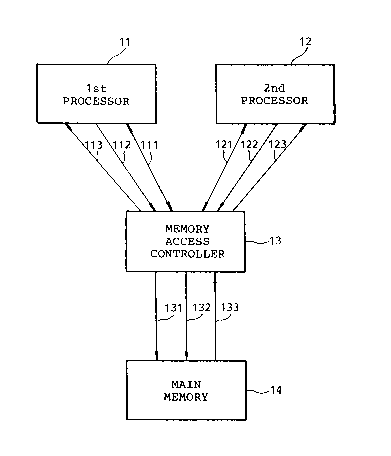
Referring to, Fig. 1, a multiprocessQr system
according to a preferred embodiment of this invention
comprises a couple of processors 11 and 12 which may be
called first and second processors, respectively, a
memory access controller 13 common to the first and the
20 second processors ll and 12, and a main memory 14
connected to the memory access controller 13. It is to
be noted that the first and the second processors 11 and
12 may not always be identical with each other, although
description will be made on the assumption that the
25 first and the second processors 11 and 12 are identical
with each other.
In Fig. 1, the first processor 11 is connected
to the memory access controller 13 through a first
2018865
request path 111, a first storage data path 112, and a
first load data path 113. Likewise, the second
processor 12 is connected to the memory access
controller 13 through a second request path 121, a
5 second storage data path 122, and a second load data
path 123.
The first and the second request paths 111 and
121 are for transmitting request information signals
from the first and the second processors 11 and 12 to
10 the memory access controller 13 or from the memory
access controller 13 to the first and the second
processors 11 and 12. The first and the second storage
paths 112 and 122 are used to transfer storage data
signals from the first and the second processors 11 and
15 12 to the memory access controller 13, respectively. In
addition, the first and the second load data paths 113
and 123 are used to transfer load or readout data
signals from the memory access controller 13 to the
first and the second processors 11 and 12, respectively.
On the other hand, the memory access controller
13 is connected to the main memory 14 through a
controller request path 131, a controller storàge data
path 132, and a controller load data path 133. The
controller request path 131 serves to transfer a request
25 information signal between the memory access controller
13 and the main memory 14 while the controller storage
data path 132 and the controller load data path 133
serve to transfer the storage data signals from the
201886~
memory access controller 13 to the main memory 14 and to
transfer the load data signals from the main memory 14
to the memory access controller 13, respectively.
Referring to Fig. 2 together with Fig. 1, a
5 processor illustrated in Fig. 2 may be either the first
processor 11 or the second processor 12 and is assumed
to be at first used as the first processor 11. In the
example being illustrated, the processor comprises an
instruction control unit 16 and four vector calculation
10 units 21, 22, 23, and 24 which will be referred to as
first, second, third, and fourth vector calculation
units, respectively, and which are specific to the
vector calculations. In addition, the illustrated
instruction control unit 16 comprises a processing unit
15 26 which carries out a scalar calculation and
calculations other than the vector calculations. The
other calculations may be, for example, an address
calculation.
The first through fourth vector calculation
20 units 21 to 24 are connected to the memory access
controller 13 through first to fourth storage lines
112-1 to 112-4 and through first to fourth load lines
113-1 to 113-4. The first through the fourth storage
lines 112-1 to 112-4 collectively form the first storage
25 path 112 while the first through the fourth load lines
113-1 to 113-4 collectively form the first load path
113. On the other hand, the first instruction control
unit 16 is connected to the memory access controller 13
2018865
through a request transmission line 111-1 and a request
reception line 111-2 both of which may be collectively
called the first request path 111.
In the illustrated example, the second processor
5 12 is assumed to be identical with the first processor
11, as mentioned before. When the illustrated processor
is used as the second processor 12, the first through
the fourth storage lines of the second storage data path
122 may be reread as 122-1, 122-2, 122-3, and 122-4 of
10 the second storage data path 122, respectively, as shown
in parentheses. Likewise, the first through the fourth
load lines of the second load data path 123 reread as
123-1, 123-2, 123-3, and 123-4, respectively, while the
request transmission line and the request reception line
15 of the second request path 121 are depicted at 121-1 and
121-2, respectively.
In addition, each instruction control unit 16 of
the first and the second processors 11 and 12 comprises
a register 31 for monitoring states of the vector
20 calculation units 21 to 24 in each of the first and the
second processors 11 and 12, respectively. More
specifically, the register 31 is set through a scan path
line (not shown) which is used, for example, on
diagnosing a fault. In this connection, contents of the
25 register 31 are representative of the number of the
vector calculation units available in each of the first
and the second processors 11 and 12. In other words,
the contents of the register 31 are representative of
2018865
configuration of the available vector calculation units
and are produced as a configuration signal. Therefore,
the register 31 has four bits arranged from a most
significant bit to a least significant bit corresponding
S to the first through the fourth vector calculation units
21 to 24, respectively. For example, when the first
through the fourth vector calculation units 21 to 24 are
available, the register 31 is set into "1111" when a
logic "1" level and a logic "0" level represent an
10 available state of each vector calculation unit and an
unavailable state, respectively. If the first vector
calculation unit 21 alone is available while the other
vector calculation units 22 to 24 are unavailable due to
occurrence of faults or the like, the first register 31
15 is set into "1000". Thus, the contents of the first
register 31 take a state selected from seven states of
"1000", "1100", "0011", "1000", "0100", "0010", and
"0001" .
In Fig. 2, the first through the fourth vector
20 calculation units 21 to 24 are operable in parallel to
one another by forming pipelines for the vector
calculations. For this purpose, each of the first
~hrough the fourth vector calculation units 21 to 24
comprises a group of vector registers for holding a
25 plurality of vector elements and a set of pipelines for
calculating addition, subtraction, multiplication,
division, logic operation, and shift operation, as known
in the art. Vector elements are successively assigned
2018865
or allocated to each of the first through the fourth
vector calculation units 21 to 24 that is put into an
available state in a predetermined order, for example,
an ascending order. Such allocation of the vector
5 elements to the first through the fourth vector
calculation units 21 to 24 is carried out by dividing
numbers assigned to the respective vector elements by
the number of the vector calculation units 21 to 24 to
obtain residues and by successively assigning the vector
10 elements specified by the residues to the vector
calculation units 21 to 24.
Let the processor illustrated in Fig. 2 be used
as the first processor 11. The storage data signals are
sent from the first through the fourth vector
15 calculation units 21 to 24 to the memory access
controller 13 through the first to the fourth storage
lines 112-1 to 112-4 while the load data signals are
sent from the memory access controller 13 to the first
through the fourth vector calculation units 21 to 24
20 through the first to the fourth load lines 113-1 to
113-4, respectively. In addition, the instruction
control unit 16 is operable to control decoding and
production of each instruction.
Decoding a vector calculation instruction, the
25 first instruction control unit 16 (Fig. 2) delivers a
vector calculation instruction to the first through the
fourth vector calculation units 21 to 24 through a first
internal instruction line 36. In this event, the first
-- 201886~
instruction control unit 16 supplies the memory access
controller 13 through the request transmission line
111-1 with the request information signal which includes
various kinds of information to be described in detail
5 later. Similar operation is carried out in the second
processor 12. In this case, the request information
signal is delivered to the memory access controller 13
through the request transmission line 121-1 (shown in
parentheses in Fig. 2).
When a sequence of vector elements is read out
of the main memory 14 as the load or readout data
signals after completion of a memory accéss operation, a
reply signal is sent from the memory access controller
13 to the instruction control unit 16 through the
15 request reception line 111-2 or 121-2. When the reply
signal is assumed to be supplied to the first processor
11, the instruction control unit 16 delivers a data
fetch instruction to the first through the fourth vector
calculation units 21 to 24 of the first processor
20 through the first internal instruction line 36. As a
result, the vector elements are successively assigned to
and fetched as the load data signals into the first
through the fourth vector calculation units 21 to 24 in
accordance with the contents of the register 31 in the
25 manner mentioned before. Thereafter, the first through
the fourth vector calculation units 21 to 24 are
processed in parallel to one another in a pipeline
fashion. It is to be noted that the vector elements are
2018865
-
11 64768-226
assigned only to the vector calculation units which are available.
Similar operation is carried out in the second processor
12 when the vector elements are read out of the main memory 14 to
be sent through the memory access controller 13 to the second
processor 12.
On the other hand, the scalar calculation and the `
address calculation are executed in the processing unit 26 of each
of the first and the second processors 11 and 12.
With this structure, the vector elements are mainly
assigned under control of the memory access controller 13 to the
first processor 11 or the second processor 12 in consideration of
the contents of the register 31 and processed by a selected one of
the first and the second processors 11 and 12 that comprises a
plurality of the vector calculation units 21 to 24. Therefore,
the vector elements can be processed at a high speed. Moreover,
the scalar calculation can be processed by the remaining processor
12 while the selected processor processes the vector elements and
may be executed independently of the selected processor.
Accordingly, a lot of jobs can be flexibly assigned to the
processors and be also processed at a high speed in the
illustrated multiprocessor system.
Referring to Figure 3, the memory access controller 13
comprises a request controller 51, an address generator
(calculator) 52, a switching circuit 53, a first alignment
controller 54, a first alignment circuit 55, a delay circuit 56, a
second alignment controller 57, and a second alignment circuit 53.
The request controller 51 is connected to the request transmission
lines 111-1 and 121-1 joined to the instruction control units 16
2018865
12 64768-226
of the first and the second processors 11 and 12 and controls the
address generator 52, the switching circuit 53, and the first
alignment controller 54 through first, second, and third internal
connections 61, 62, and 63, respectively. The request controller
51 also controls the delay circuit 56 through the third internal
connection 63. At any rate, the request controller 51 serves to
arbitrate the request information signals sent from the first and
the second processors 11 and 12 in a manner to be described later
and may be called an arbitrating circuit.
The switching circuit 53 is connected to the first
through the fourth storage lines 112-1 to 112-4 (Fig. 2) of the
first storage data path 112 extended from the first through the
fourth vector calculation units 21 to 24 and is connected to the
first through the fourth storage lines 122-1 to 122-4 of the
second storage data path 122. The switching circuit 53 is
operable to switch the first storage data path 112 and the second
storage data path 122 from one to another under control of the
request controller 51. Consequently, the storage data signals on
the first storage data path lines 112 and the second storage data
.,;. - ^
~3
2018865
13
path are selectively produced from the switching circuit
53.
The storage data signals selected by the
switching circuit 53 are sent to the first alignment
5 circuit 55 through first through fourth inner lines 66-1
to 66-4 which are collectively depicted at 66 and are
delivered to the first alignment circuit 55 controlled
by the first alignment controller 54 connected to the
request controller 51 through the third internal .
10 connection 63. The first alignment circuit 55 assigns
the storage data signals to the controller storage path
132 under control of the first alignment controller 54.
The illustrated controller storage path 132 is formed by
first through fourth controller storage lines 132-1 to
15 132-4 which are connected to memory ports of the main
memory 14.
The address calculator 52 is connected to the
request controller 51 through the first internal
connection 61 and can simultaneously produce four
20 address signals at maximum. The address signals are
sent to the main memory 14 through the controller
request path 131 which is composed of first through
fourth controller request lines 131-1 to 131-4. The
request controller 51 also controls the second alignment
25 controller 57 through the delay circuit 56 connected to
the first and the second processors 11 and 12 through
the request reception lines 111-2 and 121-2,
respectively.
2018865
14
The second alignment circuit 58 is connected to
the main memory 14 through the controller load data path
133 composed of first through fourth controller load
lines 133-1 to 133-4 and is connected to the first load
S data path 113 and the second load data path 123 extended
from the first and the second processors 11 and 12. The
second alignment circuit 58 serves to selectively
deliver the load data signals to the first and the
second processors 11 and 12 through the first and the
10 second load data paths 113 and 123 under control of the
second alignment controller 57.
As readily understood from the above, a
combination of the switching circuit 53 and the first
and the second alignment circuits 55 and 58 serves to
15 connect the vector calculation units to the main memory
14.
In operation, let the first processor 11 supply
the request information signal from the instruction
controller 16 (Fig. 2) to the memory access controller
20 13 through the request transmission line 111-1. In this
event, it is surmised that the request information
signal includes a request, a leading address of the
vector elements, the distance between two adjacent
vector elements, the number of the vector elements, a
25 command representative of a species of access
operations, and the contents of the first register 31
which are held in the instruction control unit 16 and
which are representative of the number of the vector
- 201886~
calculation units which are available in the first
processor 11 and which may be called available vector
calculation units.
The request controller 51 arbitrates the
5 requests between the first and the second processors 11
and 12 to select either one of the requests as a
selected request. Thereafter, the request controller 51
determines a maximum number of vector elements which are
simultaneously accessible by the selected request and
10 which may be called simultaneously accessible vector
calculation units. In this event, the maximum number of
the vector elements is decided by the number of the
available vector calculation units. Specifically, when
the available vector calculation units are equal in
15 number to four, the maximum number of the simultaneously
accessible vector elements is equal to four. Likewise,
when the number of the available vector calculation
units is equal to two and unity, the maximum numbers of
the simultaneously accessible vector elements are equal
20 to two and one, respectively.
Inasmuch as the request information signals are
individually sent from the respective processors, the
request controller 51 correctly calculates the number of
the simultaneously accessible vector elements at every
25 request even when the numbers of the vector calculation
units in the processors are different from one another.
The request controller 51 supplies the address
calculator 52 through the first internal connection 61
`~ 2018865
16
with the number of the simultaneously accessible vector
elements together with the leading address and the
distance between two adjacent vector elements. The
address calculator 52 calculates addresses of the vector
5 elements on the basis of the leading address, the number
of the simultaneously accessible vector elements, and
the distance. The addresses calculated by the address
calculator 52 are equal in number to the number of the
simultaneously accessible vector elements and are sent
10 to the main memory 14 through the controller request
lines 131-1 to 131-4 along with the request.
Herein, the request is assumed to be a storage
request which requests to store data signals from the
first processor 11 to the main memory 14. In addition,
15 it is assumed that first through fourth ones of the
storage data signals are sent from the first through the
fourth vector calculation units 21 to 24 (Fig. 2) to the
switching circuit 53 (Fig. 4). Under the circumstances,
the request controller 51 selects the first processor 11
20 and supplies the switching circuit 53 through the second
internal connection 62 with a switching signal
indicative of selection of the first through the fourth
storage data lines 112-1 to 112-4 of the first processor
11. As a result, the first through the fourth storage
25 data signals are sent from the switching circuit 53
through the four internal lines 66 to the first
alignment circuit 55 which is controlled by the first
alignment circuit 54.
2018865
17 64768-226
The first alignment controller 54 is supplied from the
request controller 51 through the third internal connection 63
with the leading address, the distance between two adjacent vector
elements, and the number of the available vector calculation
units. In other words, the number of the available vector
calculation units may be referred to as a configuration signal
representative of configuration of the available vector
calculation units. Responsive to the leading address, the
distance, and the number of the available vector calculation
units, the first alignment controller 54 delivers a control signal
to the first alignment circuit 55. The control signal controls
the first alignment circuit 55 so that the storage data signals on
the first through the fourth inner lines 66-1 to 66-4 are assigned
to the first through the fourth controller storage lines 132-1 to
132-4 determined by the leading address, the distance, and the
number of the available vector calculation units. Such an
alignment controller 54 and a first alignment circuit 55 may be
described in the European Patent Application Publication No. 0 189
200 which was published on January 18, 1989, and will therefore
not be mentioned any longer.
For example, it is assumed that the contents of the
first register 31 are equal to "1111" and that the leading address
of the leading one of the storage data signals and the following
address of the following one
201886~
18
of the storage data signals are made to correspond to
the memory ports of the main memory 14 connected to the
first and the second controller storage lines 132-1 and
132-2, respectively. In this event, when the
5 illustrated memory access controller 13 is accessed by
the first processor 11, the leading storage data signal
is given through the first inner line 66-1 and is
assigned to the first controller storage line 132-1 to
be supplied to the main memory 14 while the following
10 storage data signal is given through the second inner
line 66-2 and is assigned to the second controller
storage line 132-2 to be delivered to the main memory
14.
On the other hand, when the second processor 12
15 accesses the main memory 14 with the register 31 kept at
"0011", the storage data signals are sent through the
switching circuit 53 to the first alignment circuit 55
to be assigned to the third and the fourth controller
storage lines 132-3 and 132-4 on the basis of the
20 content of the register 31 (Fig. 2). Thus, the first
alignment circuit 55 assigns the storage data signals
to the third and the fourth controller storage data
lines 132-3 and 132-4 in accordance with the
configuration of the available vector calculation units
25 indicated by the register 31.
In the example being illustrated, the request
controller 51 is also connected to the delay circuit 56
through the third internal connection 63. This shows
201886~
19
that the delay circuit 56 is supplied from the request
controller 51 with the request information signal. The
request information signal is delayed by the delay
circuit 56 for an interval of time necessary for
5 accessing the main memory 14. After lapse of the
interval of time, a reply signal is sent back to the
first and the second processors 11 and 12 through the
request reception lines 111-2 and 121-2, respectively.
When the load or readout request is issued as
10 the request information signal from each processor, the
load or the readout data signals are read out of the
main memory 14 to be supplied to the second alignment
circuit 58 through the controller load data path 133
composed of the first through the fourth controller load
15 lines 113-1 to 113-4. The second alignment circuit 58
assigns the load data signals to the first load data
path 113 or the second load data path 123 under control
of the second alignment controller 57 connected to the
delay circuit 56. In this case, the second alignment
20 controller 57 is similar in structure and operation to
the first alignment controller 54 except that the
leading address, the distance, and the number of the
available vector calculation units are delayed by the
delay circuit 56. In addition, the second alignment
25 circuit 58 serves to supply the load data signals to the
vector calculation units included in the first and the
second processors 11 and 12 under control of the second
alignment controller 57 and is operable in a manner
201886~
similar to the first alignment controller 54. As a
result, the second alignment controller 57 controls the
second alignment circuit 58 so that the load data
signals are correctly assigned or distributed to the
5 first load data path 113 or the second load data path
123. More specifically, the second alignment circuit 58
is controlled so that the leading load data signal read
out of the leading address of the main memory 14 is
returned back to the vector calculation units determined
10 for the leading load data signal on the basis of the
contents of the register 31 of each processor. From
this fact, it is readily understood that the load data
signals are correctly delivered to the first and the
second processors 11 and 12 even when the vector
15 calculation units are different in number and structure
from each other.
Thus, the multiprocessor system illustrated in
Figs. 1 through 4 comprises a plurality of processors
each of which comprises at least one vector calculation
20 unit and a register for storing a configuration signal
representative of configuration of the vector
calculation unit or units. In addition, each processor
issues a memory access request including the
configuration signal. Therefore, it is possible to put
25 the processors into operation even when configuration of
the vector calculation units in each processor is
different from one another. Therefore, the
multiprocessor system flexibly assigns jobs to the
201886~
processors. Moreover, a reduction of the vector
calculation units can be minimized in the system. This
is because each register 31 of the first and the second
processors 11 and 12 individually indicates the
5 configuration of the vector calculation units.
Although the first through the fourth vector
calculation units 21 to 24 have been installed in each
of the first and the second processors 11 and 12 as
illustrated in Fig. 2, the numbers of the vector
10 calculation units may be different from each other in
the first and the second processors 11 and 12.
Referring to Fig. 4, the second processor 12
(Fig. 1) comprises a single vector calculation unit 21
which is similar in structure and operation to those
15 illustrated in Fig. 2. In addition, the second
processor 12 further comprises an instruction control
unit 16' which includes a processing unit 26' which is
similar in operation and structure to the processing
unit 26 illustrated in Fig. 2. The single vector
20 calculation unit 21 is connected to the memory access
controller 13 through the second storage data path 122
and the second load data path 123 like in Fig. 1 while
the instruction control unit 16' is connected to the
memory access controller 13 through a request
25 transmission line 121-1 and a request reception line
121-2 both of which form the second request path 121.
2018865
In the example being illustrated, the register
31 in the second processor 12 may be structured by a
single bit register and is set into "1" or "O".
The second processor 12 illustrated in Fig. 4 is
5 operable in a manner similar to that illustrated in Fig.
2 and will not be described any longer.
While this invention has thus far been described
in conjunction with a preferred embodiment thereof, it
will readily be possible for those skilled in the art to
10 put this invention into practice in various other
manners. For example, two or more processors may be
included in the multiprocessor system. In this event,
each processor may comprise a plurality of vector
calculation units which are independently controlled by
15 the memory access controller.