Language selection

Search

Patent 2019237 Summary

Third-party information liability

Some of the information on this Web page has been provided by external sources. The Government of Canada is not responsible for the accuracy, reliability or currency of the information supplied by external sources. Users wishing to rely upon this information should consult directly with the source of the information. Content provided by external sources is not subject to official languages, privacy and accessibility requirements.

Claims and Abstract availability

Any discrepancies in the text and image of the Claims and Abstract are due to differing posting times. Text of the Claims and Abstract are posted:

  • At the time the application is open to public inspection;
  • At the time of issue of the patent (grant).
(12) Patent Application: (11) CA 2019237
(54) English Title: METHOD AND APPARATUS FOR LINEARIZING THE OUTPUT OF A DIGITAL-TO-ANALOG CONVERTER
(54) French Title: METHODE ET DISPOSITIF POUR LINEARISER LE SIGNAL DE SORTIE D'UN CONVERTISSEUR NUMERIQUE-ANALOGIQUE
Status: Deemed Abandoned and Beyond the Period of Reinstatement - Pending Response to Notice of Disregarded Communication
Bibliographic Data
(51) International Patent Classification (IPC):
  • H03M 01/08 (2006.01)
  • H03M 01/06 (2006.01)
  • H03M 01/68 (2006.01)
(72) Inventors :
  • BLACKHAM, RAYMOND C. (United States of America)
(73) Owners :
  • AGILENT TECHNOLOGIES, INC.
(71) Applicants :
  • AGILENT TECHNOLOGIES, INC. (United States of America)
(74) Agent: MARKS & CLERK
(74) Associate agent:
(45) Issued:
(22) Filed Date: 1990-06-18
(41) Open to Public Inspection: 1991-05-27
Examination requested: 1997-05-09
Availability of licence: N/A
Dedicated to the Public: N/A
(25) Language of filing: English

Patent Cooperation Treaty (PCT): No

(30) Application Priority Data:
Application No. Country/Territory Date
442,278 (United States of America) 1989-11-27

Abstracts

English Abstract


METHOD AND APPARATUS FOR LINEARIZING
THE OUTPUT OF A DIGITAL-TO-ANALOG CONVERTER
Abstract of the Disclosure
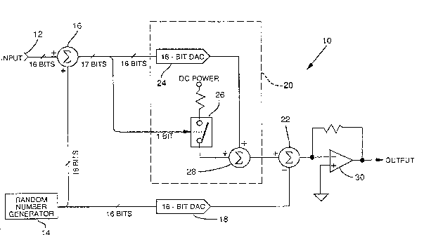
Distortion in a digital-to-analog converter (DAC)
is eliminated by adding a digital random number to
each sample of the digital signal, converting the sum
into analog form, and subtracting from this analog sum
the analog counterpart of the digital random number.
The result is the analog counterpart to the input
digital signal. The conversion of the summed digital
signal and the random number into analog form can be
performed by two conventional DACs. For any digital
input sample, the output of each DAC is equally likely
to contain any of the possible distortion errors
produced by that DAC. (An exception is the most
significant output bit of the DAC that processes the
summed signal, an exception that may be handled by
stripping off the most significant bit and applying it
to a one bit DAC.) The error signal at the output of
each of the two DACs is thus a random sequence (i.e.
noise) of DAC distortion errors. The time average of
this noise signal is a small offset error which, if
desired, can be removed by subsequent processing
stages.


Claims

Note: Claims are shown in the official language in which they were submitted.


- 6 -
I CLAIM:
1. A method of low distortion digital-to-analog
conversion comprising the steps:
providing an N bit sample of an input digital
data signal;
generating an N bit digital random number;
adding said N bit sample and said N bit random
number to yield an (N+1) bit combined digital number;
converting said N bit random number into a first
analog signal;
converting said (N+l) bit combined digital number
into a second analog signal; and
subtracting said first analog signal from the
second analog signal to produce an analog signal
corresponding to the input digital data sample.
2. The method of claim 1 in which the second
converting step comprises:
converting the most significant bit of said (N+1)
bit combined digital number into a third analog
signal;
converting the N least significant bits of said
(N+1) bit combined digital number into a fourth analog
signal; and
summing said third and fourth analog signals to
yield the second analog signal.
3. A signal processing method comprising the
steps:
providing an input data signal;
providing an input random signal;
combining said input data signal with said input
random signal to yield a combined signal; and
processing said combined signal to yield an
output signal whose mean value is a linear function of
the input data signal.

- 7 -
4. The method of claim 3 in which the input data
signal is a digital signal and the output signal is an
analog signal whose mean value corresponds to the
input data signal converted into analog form.
5. The method of claim 3 in which the input
random signal is a digital signal.
6. The method of claim 3 in which the processing
step includes:
non-linearly processing the combined signal to
produce a processed combined signal:
non-linearly processing the input random signal
to produce a processed random signal; and
subtracting the processed random signal from the
processed combined signal to yield a processed version
of the input signal.
7. The method of claim 6 in which the non-
linearly processing steps comprise converting digital
signal representations into analog signals.
8. The method of claim 7 in which the analog
signals are analog current signals.
9. The method of claim 3 in which:
the input data and input random signals are
digital signals;
the combining step comprises digitally adding
said input data signal and said input random signal to
yield a combined digital signal;
the processing step includes converting said
input random signal and said combined digital signal
into analog current signals, and subtracting said
analog signals to yield an analog output signal whose

- 8 -
mean value corresponds to the input data signal
converted into analog form.
10. The method of claim 3 in which:
the input data and input random signals are N-bit
digital signals;
the combining step comprises digitally adding
said input data signal and said input random signal to
yield an (N+1) bit combined digital signal; and
the processing step includes:
converting said input random signal into a
first analog signal;
converting the least significant N bits of
the combined digital signal into a second analog
signal;
converting the most significant bit of the
combined digital signal into a third analog
signal; and
adding the second and third analog signals,
and subtracting from the sum the first analog
signal to yield an analog output signal whose
mean value corresponds to the input data signal
converted into analog form.
11. A low distortion digital-to-analog signal
conversion system comprising:
means for receiving an input digital data signal;
a source of a digital noise signal;
combining means for combining said input digital
data signal with said digital noise signal to produce
a combined digital signal;
first converter means for converting the digital
noise signal into a first analog signal;
second converter means for converting the
combined digital signal into a second analog signal;
and

- 9 -
means for subtracting the first analog signal
from the second to yield a low distortion analog
output signal having a magnitude corresponding to the
input digital data signal.
12. The system of claim 11 in which the first
and second converter means comprise means for
converting input digital signals into output analog
current signals.
13. The system of claim 11 in which:
the combining means includes means for combining
an N-bit input digital data signal with an N-bit
digital noise signal to produce an (N+1) bit combined
digital signal; and
the second converter means comprises means for
converting the N least significant bits of the
combined digital signal into a third analog signal,
means for converting the most significant bit of the
combined digital signal into a fourth analog signal,
and means for combining said third and fourth analog
signals to form said second analog signal.

Description

Note: Descriptions are shown in the official language in which they were submitted.


2 ~3 l 3 ~ sl 9
-- 1 --
ME~OD AND APPAR~T~ ~OR ~INEARIZING
T~E O~P~T OF A DIGI~AL TO~ANALO~ CONVERTER
Field of the InventiQn
The present invPntion relates to digital-to-
analog conversion circuitry, and more particularly to
a method and apparatus for linearizing the output of a
digital-to-analog converter.
Backq~ound and Summarv of the Invention
Digital-to-analog converters (DACs) find
application in myriad electronic applications. In
some applications, it is important that the conversion
from digital to analog be highly accuratP. Exemplary
are signal analysis instruments that must produce
highly accurate analog excitation signals ~rom
corresponding digital signal data. In most such
applications, conversion errors that are a function of
the input digital data ~hereafter referred to as
distortion) are much more important than errors that
are uncorrelated ~hereafter referred ~o as noise).
The noise portion of any conversion error can always
be reduced by averaging the waveform over time. The
distortion portion of the error, however, cannot.
To achieve low distortion D/A conversion, resort
must usually be made to precision DACs that have been
fabricated with finely matched componsnts. An
a-ternative approach is to quantify the distortion
error of a particular converter at all possible input
signal conditions and then to implement a correction
circuit that compensates for the circuit's known
error. Both approaches, however, are expensive and
unsuitable for large volume production.
The present invention achieves accuracy
comparable to that achieved with the precision
approaches, but employs readily available off-the-
shelf components.

According to the present invention, the input
signal to be applied to a conventional DAC is first
processed so that its value is uncorrelated with that
of the unprocessed input signal. This processing can
be effected by adding a digital random, or pseudo-
random num~er to the input digital signal. The
digital random number is then converted into analog
form by a first DAC, and the processed sum is
converted into analog form by a second DAC. An analog
subtraction circuit then subtracts the analog version
of the random number from the analog vexsion of the
process~d sum. The difference is the analog
counterpart to the original digital input signal.
For any digital input sample, the output of the
first DAC is equally likely to contain any of the
possible distortion errors produced by that VAC. 'rhe
same is true for the output of all except the most
significant bit of the second DAC. The most
significant bit has some correlation to the input
signal. 'rO segregate the effects of this bit, it is
desirably stripped off and applied to an third, one-
bit DAC. This leaves the outputs of the first and
second ~ACs both uncorrelated with the original
digital input signal, meaning their output error
signals are random sequences (i.e. noise) composed of
DAC distortion errors. The ensemble of this noise
signal is a small constant, termed an offset error.
If desired, this small offset error can be removed by
subsequent processing stages.
The ~oregoing and additional features and
advantages of the present invention will be more
readily apparent from the following detailed
description thereof, which proceeds with reference to
\ the accompanying Figure.

Bria~ Description of the Fiqure
The Figure is a schematic block diagram of a DAC
linearizing circuit according to ons embodiment o~ the
present invention.
_tailed Descript on
~ eferring the Figure~ a DAC linearizing circuit
10 according to one embodiment of the present
invention includes a digital data signal input 12, a
random noise generator 14, a digital adder 16, first
and second digital-to-analog converters (DACs) 18, 20,
and an analog combining circuit 22.
In operation, a digital signal to be converted
into analog form is applied to the digital si~nal
input 12. In a representative embodiment, this signal
may be 16 bits in width, although the invention is not
so limited. The adder 16 adds to each sample of the
input digital signal a digital random number o~ equal
width, here 16 ~its, ~rom the random number generator
14. Since both signals applied to the adder have 16
bits, the output sum is a 17 bit value.
The system next con~erts the summed digital
signal and the digital random number into analog
signals using DACs 20 and 18, respectively. Finally,
the analog combining circuit 22 subtracts from the
analog version of the summed signal the analog version
of the random signal to produce as its output signal
an analog version of the input digital data signal.
In greater detail, the illustrated second DAC 20
here comprises a 16-bit DAC 24 that operates in
conjunction with a 1 bit DAC (or analog switch) 26.
In this arrangement, the most significant bit of the
17 bit digital sum output by the adder 16 is stripped
off and is applied to the 1-bit DAC 26. The remaining
16 bits are applied to the 16-bit DAC 24. The outputs
of these two DACs are analog current signals that are
summed by an analog summing circuit 28 to produce an

y~
analog output signal representative of the 17 bit
summed digital signal. (It will be recognized that in
other embodiments, a 17-bit D~C may be used if the
correlation of th~ most significant output bit to the
original digital input signal [discussed below] is
addressed otherwise or is ignored.)
The output of the analog summing circuit 28 i5
applied to one input of the analog col~ining circuit
22. To the second input of this combining circuit is
applied an analog current signal produced by the DAC
18 (i.e. an analog version of the digital random
number~. The resulting difference signal is applied
to an operational amplifier 30 that produces as its
output signal an analog voltage signal. This voltage
output signal is the analog counterpart to the dig:ital
data input signal.
For any digital input sample, the output of each
of the two 16-bit DACs 18, 24 is equally likely to
contain any of the possible distortion errors produced
by that DAC. The error signal at the output of each
of these DACs is thus a random sequence (i.e. noise)
of DAC distortion errors. The ensemble of this noise
signal is a small constant, termed an offset error.
Thus, on average, only an of~set error and
uncorrelated noise can be added to the analog output
signal by the 16-bit DACs 18, 24 for any given output
sample. This is true for settling errors as well.
Since consecutive random numbers from random number
generator 14 are uncorrelated to the input samples and
to each other, this error is also uncorrelated noise
and has a constant average value.
The output of the 1-bit DAC 26 is somewhat
correlated to the input digital sequence. However,
since it is a one bit DAC, only gain and offset errors
are possible. Second and higher order distortion
errors are not possible for a perfectly stable l-bit
DAC (e.g. one that doesn't drift with temperature and

time). If settling errors, such as slew rate, are
considered, a nonlinear term can appear, but will only
cause a slight linear filtering of the signal if the
sattling errors in both directions are matched (e.g.
slew rate the same in both directions). Such linear
filtering modifies the signal in a manner that can
readily be corrected by a linear analog or digital
filter.
In sum, the only errors appearing in the analog
output signal are gain errors, offset errors,
artifacts of linear filtering (due to settling
errors), and uncorrelated noise. The output is
therefore a random variable with a mean that is a
linear function of the input (e.g. with no second or
higher order terms in its polynomial expansion),
coupled with a linear filtering effect. The error
terms can be ~urther reduced in amplitude by averaging
or other forms o~ linear filtering if desired.
Having described and illustrated the principles
of my invention with reference to a preferred
embodiment, it should be apparent that the invention
can be modified in arrangement and detail without
departing from such principles. Accordingly, I claim
as my invention all such modifications as may come
within the scope and spirit of the following claims
and equivalents thereto.

Representative Drawing
A single figure which represents the drawing illustrating the invention.
Administrative Status

2024-08-01:As part of the Next Generation Patents (NGP) transition, the Canadian Patents Database (CPD) now contains a more detailed Event History, which replicates the Event Log of our new back-office solution.

Please note that "Inactive:" events refers to events no longer in use in our new back-office solution.

For a clearer understanding of the status of the application/patent presented on this page, the site Disclaimer , as well as the definitions for Patent , Event History , Maintenance Fee  and Payment History  should be consulted.

Event History

Description Date
Inactive: IPC from MCD 2006-03-11
Application Not Reinstated by Deadline 2001-12-31
Inactive: Dead - No reply to s.30(2) Rules requisition 2001-12-31
Deemed Abandoned - Failure to Respond to Maintenance Fee Notice 2001-06-18
Inactive: Abandoned - No reply to s.30(2) Rules requisition 2000-12-29
Inactive: S.30(2) Rules - Examiner requisition 2000-06-29
Letter Sent 2000-06-22
Inactive: Multiple transfers 2000-04-20
Inactive: Correspondence - Formalities 2000-03-08
Amendment Received - Voluntary Amendment 1999-05-20
Inactive: S.30(2) Rules - Examiner requisition 1999-02-25
Inactive: Correspondence - Formalities 1999-02-09
Inactive: Status info is complete as of Log entry date 1997-10-09
Inactive: Application prosecuted on TS as of Log entry date 1997-10-09
Inactive: Delete abandonment 1997-10-09
Inactive: Abandon-RFE+Late fee unpaid-Correspondence sent 1997-06-18
All Requirements for Examination Determined Compliant 1997-05-09
Request for Examination Requirements Determined Compliant 1997-05-09
Application Published (Open to Public Inspection) 1991-05-27

Abandonment History

Abandonment Date Reason Reinstatement Date
2001-06-18

Maintenance Fee

The last payment was received on 2000-06-09

Note : If the full payment has not been received on or before the date indicated, a further fee may be required which may be one of the following

  • the reinstatement fee;
  • the late payment fee; or
  • additional fee to reverse deemed expiry.

Patent fees are adjusted on the 1st of January every year. The amounts above are the current amounts if received by December 31 of the current year.
Please refer to the CIPO Patent Fees web page to see all current fee amounts.

Fee History

Fee Type Anniversary Year Due Date Paid Date
Request for examination - standard 1997-05-09
MF (application, 7th anniv.) - standard 07 1997-06-18 1997-06-03
MF (application, 8th anniv.) - standard 08 1998-06-18 1998-06-02
MF (application, 9th anniv.) - standard 09 1999-06-18 1999-06-15
Registration of a document 2000-04-20
MF (application, 10th anniv.) - standard 10 2000-06-19 2000-06-09
Owners on Record

Note: Records showing the ownership history in alphabetical order.

Current Owners on Record
AGILENT TECHNOLOGIES, INC.
Past Owners on Record
RAYMOND C. BLACKHAM
Past Owners that do not appear in the "Owners on Record" listing will appear in other documentation within the application.
Documents

To view selected files, please enter reCAPTCHA code :


To view images, click a link in the Document Description column. To download the documents, select one or more checkboxes in the first column and then click the "Download Selected in PDF format (Zip Archive)" or the "Download Selected as Single PDF" button.

List of published and non-published patent-specific documents on the CPD .

If you have any difficulty accessing content, you can call the Client Service Centre at 1-866-997-1936 or send them an e-mail at CIPO Client Service Centre.


Document
Description 
Date
(yyyy-mm-dd) 
Number of pages   Size of Image (KB) 
Description 1997-08-14 7 255
Description 1999-05-19 7 269
Claims 1999-05-19 2 78
Drawings 1994-04-08 1 16
Abstract 1994-04-08 1 32
Claims 1994-04-08 4 120
Representative drawing 1999-07-15 1 12
Courtesy - Abandonment Letter (R30(2)) 2001-03-11 1 169
Courtesy - Abandonment Letter (Maintenance Fee) 2001-07-15 1 182
Correspondence 1999-02-08 1 36
Correspondence 2000-03-07 1 29
Fees 1996-02-21 1 48
Fees 1995-03-01 1 62
Fees 1994-02-24 1 36
Fees 1993-02-17 1 38
Fees 1992-02-16 1 40