Note: Descriptions are shown in the official language in which they were submitted.
` -
- 2 - 20 1 93~ 1
RACRGROUND OF THE lNv~ ON
The present invention relates to a negative
temperature coefficient (i.e. NN.T.C. N ) thermistor
for use in temperature measurement, control, and
compensation of electronic elements or circuits.
A typical N.T.C. thermistor i8 shown in U.S.
Patent No. 4,786,888. This patent discloses a therm-
istor element produced through sintering ceramic in
the form of a chip. It is sandwiched by a pair of
electrodes and enclosed in an envelope made of glass.
In this regard, the device only operates to secure or
stabilize the thermal or chemical properties of the
thermistor element when the thermistor is used for
measuring temperature.
A thermistor of the above type has many drawbacks
requiring relatively complex production processes,
low production capacities, poor yields, and unneces-
sary diffusive boundary layers. In addition, such
thermistor elements require leads which require
connections to external devices. This makes diffi-
cult the assembly of the thermistor element onto a
circuit board.
A less difficult way to build a surface mounted
thermistor element which would secure the thermal,
chemical and solderability properties would be envel-
~,,
- 20 1 933 1
-- 3 --
material. This low R dielectric material, which is
low fire and acid resistant, would accept æilver
electrodes that are compatible with nickel, and Sn/Pb
plating. This eliminates the need for complex pro-
duction processes, poor yields, and unnecessary
diffusive boundary layers.
Therefore, a principal object of this invention
is to provide a surface mount thermistor element that
would maintain thermal, chemical, and solderability
properties, and which is more reliable.
A further object of this invention is to provide
a method of making a thermistor which is economical
and efficient, and which will not be detrimental to
the resulting product.
A further ob~ect of the present invention is to
provide a negative temperature coefficient ceramic
material that can be plated with nickel and tin
(Sn)/lead (Pb) plating for surface mount applica-
tions.
A still further object of this invention is to
provide a negative temperature coefficient thermistor
with production processing steps which has an enve-
lope of low R insulating dielectric for enclosing the
thermistor for surface mount applications.
A still further object of the present invention
is to provide a thermistor of the above type suitable
4 20 1 933 1
for soldering directly onto a printed circuit board
for surface mount applications.
A still further object of the present invention
is to provide a thermistor which is stable in opera-
tion at higher operating temperatures for surface
mount applications.
A still further object of the present invention
is to provide a method of producing thermistors in
high volumes and with excellent yields.
These and other objects will be apparent to those
skilled in the art.
SUNMARY OF THE lwv~ ON
The N.T.C. thermistor of this invention
comprises: (1) a sintered thermistor ceramic chip,
(2) an insulating low K dielectric for enclosing the
thermistor chip to be coupled after sintering to the
ceramic chip, (3) and a pair of external electrodes,
silver plateable, on the exterior surface of the
ceramic chip and the insulating low K dielectric.
Specifically, the insulating ceramic envelope is made
of an oxide or different variety of oxide ceramic
materials. Furthermore, the external electrodes are
made out of plateable silver.
In a preferred form, a sintered ceramic wafer has
a low K A1203 or ceramic oxide loaded (sprayable
'~g
20 1 933 1
rheology) sprayed onto the top and bottom surfaces of
the wafer. The material is dried and fired in a
continuous furnace. Specifically, the material dried
in an infrared or convection oven and sintered in an
infrared or convection furnace. Atmospheric condi-
tions during firing are in either an oxidizing or
neutral atmosphere.
Once the low K dielectric has been vitrified onto
the N.T.C. ceramic wafer, the wafer i8 cut into
strips or chips. The strips and chips are either
sprayed or dipped in a sprayable or dippable rheology
to encApsulate the remaining uncovered areas of the
strips or chips. The strips or chips are fired in a
continuous infrared or convection kiln. Strips are
cut into individual ceramic chip~.
The above devices in chip form, are dipped in a
dippable silver rheology to e~rApsulate the N.T.C.
thermistor chip surfaces which are not encapsulated
with a low K dielectric.
The above devices in a negative temperature
coefficient thermistor chip form, are then provided
with terminals by being plated with a nickel (Ni)
barrier, followed by a tin (Sn)/lead (Pb) plating
onto the surface of the nickel. The parts with
silver termination are dried in an infrared or
convection oven and are fired in a continuous infra-
, ", - .
`- 20t 9331
-- 6 --
red or convection furnace. The silver termination
provides a conductive path through the thermistor
ceramic chip. The external termination and plating
on the thermistor chip will allow the thermistor chip
to be mounted directly onto a printed circuit board.
The essence of this invention is to provide a
nickel barrier over silver using conventional plating
techniques without adversely affecting the thermistor
ceramic material and its inherent electrical proper-
ties.
BRIEF DESCRIPTION OF THE DRAWINGS
Fig. 1 is a perspective view of a ceramic wafer
with an insulating dielectric material on the top and
bottom surfaces thereof;
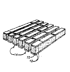
Fig. 2 is a perspective view of the ceramic view
of Fig. 1 after it has been cut into a plurality of
elongated strips;
Fig. 3 is an enlarged scale perspective view of a
thermistor ceramic chip material with an insulating
dielectric material on the top and bottom surface
created by cutting one of the strips of Fig. 2 into
shorter increments;
Fig. 4 is a perspective view of one of the strips
of Fig. 2 encapsulated within an insulating dielec-
tric material;
20 t 933 ~
-- 7 --
Fig. 5 is a perspective view of a sintered
thermistor chip encapsulated with an insulating
dielectric material and created by cutting the strip
of Fig. 4 into shorter incrementæ;
Fig. 6 is a perspective view of the chip of Fig.
5 with end caps thereon and mounted on a circuit
board;
Fig. 7 is an enlarged scale sectional view taken
on line 7-7 of Fig. 6; and
Fig. 8 is an elongated sectional view taken on
line 8-8 of Fig. 6.
DE~ATT~n DESCRIPTION OF THE PREFERRED EMBODIMENT
Fig. 1 shows a ceramic wafer or layer 10 with
dielectric layers 12 affixed to the upper and lower
surfaces thereof. The wafer 10 is a negative temper-
ature coefficient ceramic material made from materi-
als such as Nn23' NiO~ Co304, A1203, Cu0, and Fe203.
The dielectric layers 12 are comprised of a materialsuch as a low K A1203 or ceramic oxide loaded dielec-
tric. A low K A1203 or ceramic oxide loaded dielec-
tric is used because they are acid resistant which
protects the thermistor wafer 10 from acid during the
plating process.
The layer 10 is created by adding Mn203, NiO,
Co304, A1203, Cu0, or Fe203 to a slurry of organic
'5.~
201 9331
-- 8 --
binder, plasticizer, lubricant, solvent and disper-
sant. Uncured sheets of this material each having a
thickness of 100 um are prepared by the conventional
doctor blade method. The uncured sheets are stacked
together and are made into monolithic form by apply-
ing pressures thereto between 3,000 - 30,000 p.s.i.,
and under temperatures between 30 - 70 C., for a
period between 1 second to 9 minutes. The resulting
monolithic form, layer 10, is then fired at a rate
between 10 - 60 C./hr to a temperature of 1000 C. -
1300 C. for about 1 hour to 42 hours an controlled
cool down rate of 20 - 100 C./hr to become a sintered
negative coefficient thermistor. With this proces~,
the layer 10 comprises a monolithic sintered thermis-
tor body.
After the layer 10 i8 SO created, the dielectric
layers 12 are applied to the top and bottom surfaces
thereof with sprayable rheology. Layers 12 comprised
of low R A1203 or ceramic oxide loaded dielectric are
then dried in an infrared or convection oven at a
temperature of 75 C.-200 C. for 5 minutes to 1 hour.
They are then fired in an infrared or convecLion
furnace to a temperature of 700-C. - 900-C. for S
minutes to 1 hour. The resulting device of Fig. 1
can then be cut into individual strips 14 or into
chips 14A (see Figs. 2 and 3~.
~,.,
9 20 1 933 1
The uncoated sides of the strips 14 or chips 14A
can then be sprayed or dipped with the same material
comprising layers 12 to create dielectric layer 16.
After this has been done, the strips 14 or chipæ 14A
units are then fired in an infrared or convection
oven to a temperature of 75-C. - 200-C. for 5 minutes
to 1 hour, and then fired in an infrared or convec-
tion furnace to a temperature of 700-C. - 950-C. for
5 minutes to 1 hour. This procedure produces for
strips 14 and chips 14A a vitrified dielectric enve-
lope 18 of low R A1203 or ceramic loaded dielectric
on four sides of the thermistor body. Chips 14A can
be cut from the elongated strips 14.
Terminal caps 20 are then created on the ends of
the strips 14 or the chips 14A. The ends are first
dipped in plateable silver termination material 22 so
that the ends of the wafer layer 10 are in direct
contact therewith. The silver termination material
22 has an undried band width of 45 um to 800 um and
are prepared by the doctor blade method. After the
silver termination 22 has been so applied, the strips
14 or the chips 14A are dried in an infrared or
convection oven at a temperature of 100 - 300-C. for
5 - 35 minutes. They are then fired in an infrared
or convection furnace at a temperature of 500 -
700 C. for 5 to 25 minutes.
.~
_ 2019331
-- 10 --
The silver t~r~;nAtion material 22 is then plated
with a barrier layer 24 comprised of Ni having a
thickness of 100 - 500 u inches. Layers 25A and 25B
are then imposed on the layer 24 by plating. Layer
25A is comprised of Sn and layer 25B is comprised of
Pb. Layers 25A and 25B have a total thickness of
100 - 500 u inches.
The strip 14 shown in Fig. 4 completely
encapsulated in envelope 18 is identified by the
numeral 26. The completed chip 14A completely encap-
sulated in envelope 18, as shown in Fig. 5, is iden-
tified by the numeral 28. The terminal caps de-
scribed heretofore can be applied to either the
strips 26 or the chips 28.
The completed strips 26 or chips 28 can be
directly soldered to the circuit board 30 as shown in
Fig. 6.
By using the above mentioned materials and
processes, a thermistor is created which has a small-
er variance in resistance and has ideal soldering
characteristics for mounting on printed circuit
boards. This invention enables the production of
thermistors having good quality, stability, and a
higher yield rate.
It is therefore seen that the device and method
of this invention achieve all of their stated objec-
tives.
.~,