Note: Descriptions are shown in the official language in which they were submitted.
2~1~'~~~
-1-
7570
CALIBRATION SYSTEM AND METHOD FOR COLOR IMAGE SCANNING
BACKGROUND OF THE INVENTION
This invention relates to electronic image
scanning and processing and, more particularly, to the
calibration of photodetector output to compensate for
intensity and color temperature variation in subject
illumination by a low-cost source of illumination.
Canadian Patent Application Serial No. '
2009286.6 discloses a color balanced imaging system in
which plural (e.g. 3) sets of photodetectors are
exposed to a light image reflected from a subject,
which may be represented by a color photograph, for
example, in a manner to achieve a high resolution,
accurate color rendition of the image in digital form.
The photodetector sets are exposed by scanning the
subject image with white light so that light reflected
from a given picture element or "pixel" in the subject
image will impinge each individual photodetector
located in the scanning path. To this end, the
photodetectors in each set are arranged in adjacent
rows transverse to the scanning path and in columns
parallel to that path. Where the subject reflects
only light in the visible spectrum, each set of the
photodetectors is exposed through a filter which could
represent one of the primary colors, that is, red (R),
green (G), or blue (B). Alternatively, the filters
could represent the complimentary colors.
Color balance in the system of the aforea
mentioned co-pending application is achieved by a
combination of selecting the number of photodetector
rows in each set to correspond with the sensitivity of
the photodetectors to the light in the R, G and B
spectral regions and by accumulating the charge
developed by photodetectors in each column of each set
so that the output signal fox each subject image pixel
_2_
is the composite output of the photodetector rows.
For example, the photodetectors are most sensitive to
red light and least sensitive to blue light. Thus,
the photodetector set exposed through the red filter
will have as few as six active rows of photodetectors
where as the blue set will have as many as sixteen
photodetector rowa. As light reflected from each
image pixel scans or traverses the photodetectors in a
column common to all three sets, the R, G or B
spectral components in the pixel develop a charge in
each phatodetector underlying a filter which passes a
spectral component in the pixel. The photodetector
charges are accumulated in each photodetector set in a
manner such that each successive photodetector in a
column receives the charge of a photodetector
immediately preceding it in the context of scanning
direction and also adds its own charge to the
accumulating charge. As a result of the accumulation
of charges, each image pixel is represented by a well
developed photodetector signal capable of being
processed electronically to develop a digital
emulation of the subject image. Moreover, an
exceedingly high measure of color balance is achieved
simply by variation in the number of photodetectors
exposed to the respective R, G and B spectral
components of each subject image pixel.
While the afore-mentioned scanning system
represents a major advance inythe attainment of data
accurate with respect to color balance, the overall
quality of data obtained by image scanning is
dependent also on uniform intensity and color
temperature of the source of the illumination
reflected from the subject image to the photodetector
sets. zf a low-cost tungsten halogen bulb powered by
line voltage, for example, is used as the source of
image scanning illumination, the intensity of light
reflected from the subject image to the photodetectors
~03.~'~2
_3_
will vary with normal?.y incurred line voltage
variations including the sixty cycle ripple associated
with line voltage. Also, the color temperature of
such a light source is unstable particularly during
the period immediately after the lamp is turned on.
Quite obviously, the signals generated by the
photodetectors exposed to such a light source will
vary with the voltage variation induced intensity of
the light, and with color temperature variation where
photodetector signal strength is predicated on
response to a limited spectrum of the reflected light.
The problems associated with intensity and
color temperature variation in low-cost light sources
for image scanning applications have been addressed in
the prior art. Fox example, U.S» Patent No. 4,174,528
and the prior art cited therein as background art
teach the use of a white reference image or patch in
the light path between the light source and a
photodetector array for the purpose of calibrating the
output of the array to compensate for variations in
exposure light intensity and color temperature. In
many of the prior art disclosures, the white reference
patch is exposed to the photodetectors only at the
beginning of an image scan. It is obvious that this
approach to photodetector calibration is effective
only in a very general way and would not account for
cyclical variations in light intensity variations
which occur during the scan of a single subject image.
The disclosure of U.S. Patent No. 4,174,528, on the
other hand, approaches a scanner calibration procedure
by which photodetector calibration is accomplished on
a line-by-line basis. Specifically, a linear detector
array provided for reading the document or subject
image includes a detector in the path of light
reflected from reference indicia and associated with
an exposure meter circuit. When light reflected from
a given line of image pixels is read by the
~0~.~°'~~~
-4
photodetector array, 'the quantity of light read by the
exposure meter associated detector is integrated and
stored in a manner to control the exposure of the
image sensing photodetectors in the next line of
pixels. This system operates in the manner of an
electronic shutter by which the time during which the
detectors are exposed to light reflected from the
subject image is controlled by the exposure meter
circuit.
From the standpoint of adapting the exposure
control arrangement of the afore-mentioned U.S. Patent
No. 4,174,528 to the system described with reference
to the afore-mentioned co-pending patent application
in which the charges developed by individual rows of
photodetector cells are accumulated to achieve color
balance, several problems arise. For example, where
the photodetector cell charges are accumulated in
successive rows, it is essential that the rate of
photodetector charge transfer is identical to the rate
of image pixel scan. Although it might be possible to
vary the rate of scan to accommodate a variable
exposure time interval for each row of photodetectors,
the costs of doing so are likely to be greater than
the costs of a non-variable light source. Also, the
resolution requirements for reproducing a subject
image represented by a color photograph, for example,
require a photodetector cell density of a magnitude
making it extremely difficult to accommodate circuity
associated with electronic shutter operation.
Finally, the attainment of digital data capable of
reproducing a high resolution subject image, such as a
color photograph, requires that photodetector cell
calibration be accomplished on a real time basis, that
is, so that the phatodetector cells in each row
scanned by the subject image are calibrated on the
basis of light to which they are actually exposed.
4
2~~.9~~~~
-5-
Tn light of 'the foregoing, it will be seen
that there is a need for an effective photodetector
calibration system for the color balanced scanning
technique of the type in which photodetector output is
the result of the transfer and accumulation of~'
successive cell charges.
SUMMARY OF THE TNVENTION
2n accordance with the present invention, a
system is provided for calibrating the output of image
scanning photodetector cells to compensate for
variations in light emanating from a low-cost light
source, on a real time basis, and in a manner enabling
the use of a sufficiently dense pattern of cells to
obtain a high resolution digital replica of an image
exemplified by a color photograph. Where the image
scanner employs an accumulating charge transfer
arrangement of photodetector rows, the first few cells
in each photodetector row are exposed to illumination
reflected from a white reference patch in a manner so
that any variation of charge produced by those cells
from an arbitrary normal value is used as a
calibration factor for the image light scanned cells
in the same row.
The invention is practiced by serially traps-
ferring the charge signals of each photodetector row
to a multiplying processor. The signals resulting
from exposure of the first few photodetector cells in
a row to the white reference sample are multiplied by
1 and the value compared with a constant reference
value. The constant reference value is divided by the
incoming white reference signal value to achieve a
calibration factor. As the signals developed by
photodetector cells in the same row but scanned by
subject image pixels are fed to the processor, they
are multiplied by the calibration factor to correct
for exposure light intensity variations from that
represented by the constant reference value.
~~~~"l~ i
-6-
In a photodetector array which includes sets
of photodetector rows and transfer circuitry for
accumulating the cell charges developed by the image
illumination scan, the provision of white reference
patch reading cells in each row of a set results in an
accumulation of white reference charges corresponding
directly to the accumulated charges of image pixel
reading cells. When the set is exposed through a
filter passing light of a limited spectral region,
such as red, green or blue light, variations in
illumination color temperature will be accounted for
as variations in intensity at each row of
photodetector cells. Because the calibration for
light intensity variation is performed on the raw
signal data transferred from the photodetectors and
because all photodetector cells in each row, including
cells reading image pixels and cells reading the white
reference patch, are expased by the same line
increment of illumination, variations in that line
increment of illumination caused by fluctuations at
the light source may be measured and corrected in real
time for each line of photodetectors scanned.
A principal object of the present invention
is, therefore, the provision of an improved
calibration system and method by which the output of a
photodetector array scanned by imaging illumination
originating in a low-cost and variable light source
may be corrected in real time to obtain data guality
commensurate with precisely uniform illumination
sources. Another abject of the present invention is
to provide such a calibration system and method which
enables the use of a dense pattern of photodetectors
consistent with providing digital data replicas of
high resolution color photographs. Still another
abject of the present invention is to provide a
photodetector calibration system and method suitable
for use with color balanced image scanning
~~~.~"~~~
photodetector sets in which each of multiple sets
includes a variable number of photodetectors depending
on photodetector sensitivity to differing spectral
regions of light. Other objects and further scope of
applicability of the present invention will become
apparent from the detailed description to follow taken
in conjunction with the accompanying drawings in which
like parts are designated by like reference numerals.
BRIEF DESCRIPTION OF THE DRAWINGS,
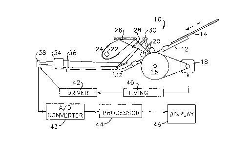
Fig. 1 is a schematic side elevation of com-
ponents used in an image scanner with which the
present invention is particularly suited for use;
Fig. 2 is a schematic plan view of the
optical system employed in the apparatus of Fig. 1;
Fig. 3 is a front elevation depicting the
physical arrangement of photodetector sets used in the
image scanning device of Fig. 1;
Fig. 4 is a fragmentary schematic view
depicting operation of the photodetector array
employed by the present invention;
Figs. 5A and 5B are block diagrams
representing identical components but in different
states of operation.
DETAILED DESCRIPTION OF THE PREFERRED EMBODIMENT
In Figs. 1 and 2 of the drawings, an image
scanning apparatus is generally designated by the ,
reference numeral 10 and shown to include components
substantially identical to those disclosed in the
afore-mentioned co-pending U.S. patent application
Serial No. 328,314. While the system 10 is
substantially fully disclosed in the a:fore-mentioned
co-pending application, the general organization and
operation of the system is worth repeating here in the
interest of a full understanding of the calRibration
system of the present invention.
Thus, in Fig. l, the scanning system 10 is
shown to include a bed 12 on which a subject 14 is
~~1~'~2a
placed for engagement by a rotatable drum 16 driven by
a stepping motor 18. The subject 14 passes between
the periphery of the drum 16 and a pair of pressure
rollers 20 in a manner to attain a secure frictional
engagement of the subject 14 between the drum 16 and
the rollers 20. A source of illumination, represented
by a tungsten halogen tube 22 positioned within a
focusing reflector 24, develops a path of illumination
from the bulb 22 to the section of the drum periphery
located between the pressure rollers 20 with the aid
of a mirror 26 and a polarizes 28. Illumination
reflected from the same peripheral region of the drum
16 is folded by mirrors 30 arid 32 and passed to a
focusing lens 34 through a second polarizes 36.
Illumination focused by the lens 34 is passed to a
photo detector array 38 to be described in more detail
below. As depicted in block diagram form in Fig. 1,
the system includes an electronic timing device 40
such as a clock generator which outputs to the steppei
motor 18 and to a driver 42 for the photodetector
array 38 to synchronize operation of the motor and the
photodetector array 38 in a manner to be described in
more detail below. Output from the photodetector
array 38 is digitized by way of an analog to digital
(A/D) converter 43 and then fed to a processor 44 and
ultimately to a display 46, again in a manner to be
described in more detail below.
The folded path of illumination from the bulb
22 to the photodetector array 38 is generally depicted
in the plan view of Fig. 2 of the drawings. The
illustrated illumination path represents a departure
from the illumination path of the image scanning
system disclosed in the afore-mentioned co--pending
application in that, in addition to light reflected
from the image on the subject 14 as it passes over the
drum 16, illumination is also reflected from a white
reference patch 48 which may be represented in
~0~~~~~
_g_
practice by a stationary white patch of dimensions
corresponding to the width of the illumination scan at
the periphery of the drum 16 but located on the
housing (not shown) which supports the drum 16 fox
rotation. The white reference patch 48 may take other
physical forms such as a white band on the edge of the
drum 16 adjacent to the position of the drum occupied
by the subject 14 or it may be represented by a white
border along one longitudinal edge of the subject 14.
Regardless of the specific physical form taken by the
white reference patch 14, it represents a reference
patch of white light by which illumination originating
with the bulb 22 is reflected through the lens 34 and
focused along one edge of the photodetector array 38
simultaneously with light reflected from the image on
the subject 14.
In Fig. 3 of the drawings, the physical or-
ganization of the photodetector array 38 is depicted
in relation to a single row of pixels reflected from
the subject 14 and the white patch 48. Tt should be
noted with respect to Fig. 3 that while the pixels are
shown as arranged on a single line, the image elements
or pixels on the subject, as well as in the reflected
light image of the subject forwarded by the lens 34,
are randomly distributed in accordance with the image
information they represent. On the other hand,
because of the geometry of the photodetector cells in
the array 38, the pixels are resolved into a series of
adjacent linear rows not unlike the single row
illustrated in Fig. 3.
The photodetect.or array 38 is similar to that
disclosed in the afore-mentioned co-pending
application in that it is comprised of three
photodetector sets or circuit modules 50, 52 and'54. w
Each module contains sixteen rows 56 of photodetector
cells, the rows being oriented transverse to the
direction of image scan as represented by the arrow
:7:-.
~~~.~"~~~
58. The individual cells in the rows 56 are also
arranged to be aligned as columns which extend
parallel to the direction of image scan. Although not
illustrated in Fig. 3 of the drawings, each of the
modules 50, 52 and 54 is covered by a filter (not
shown) corresponding to the basic red, green and blue
spectral regions of visible light. Specifically, the
module 50 includes a red falter which covers all of
the active cells thereof whereas the module 52 is
exposed through a green filter and the module 54
through a blue filter. Because the photodetector
cells are most sensitive to red light and least
sensitive to blue light, the red module 50 is covered
with a mask 60 leaving only six active rows 56 of
photodetector cells. In the blue module 54, all
sixteen rows 56 are active whereas in the green module
52, a mask 61 is again incorporated to expose only
twelve active rows 56 of photodetector cells.
Tn the illustration of Fig. 3, the first two
columns of photodetector cells in each module 50, 52
and 54 are stippled to delineate them from the other
columns of photodetector cells. While the stippled
cells are identical in all respects to the other
cells, they are delineated because they are exposed to
light reflected from the white reference patch 48
whereas the other cells are exposed to light reflected
from the subject 14. While the first two ae7.ls are
shown as reserved for exposure by light reflected from
the white patch 48, it is contemplated that as many as
20 columns of pixels may be used for this purpose.
Also in Fig. 3, the final row 57 in each module 50, 52
arid 54 is delineated by cross-hatching and while
comprising the same Cells as the rows 56, is provided
with circuitry to be described and by which it
functions as a shift register.
The basic operation and circuity of the
photodetector sets or modules 50, 52 and 54 may be
-11-
appreciated by reference to Fig. 4 in which a vastly
enlarged fragment of 'three detector rows 56 and a
shift register 57 are shown. With the exception of
the color filter associated with each module and the
masks 60 and 61 of the modules 50 and 52, each of the
modules 50, 52 and 54 is identically constructed.
In Fig. 4, the subject 14 is shown as having
an arbitrary shape extending from one linear edge 14e
and :further includes two rows of two pixels each. The
pixels are presented as little circles identified by
the legends A1,A2 in the first row, and B1,B2 in the
second row. A single reference pixel (REF) is shown
as aligned with the row A1,A2 of image pixels and is
presented in the light image to which the modules 50,
52 and 54 are exposed by the same linear increment of
light as the image pixels in that row. In this
respect, while the white reference patch 48 from which
the reference pixel emanates may remain stationary
while the subject 14 is moved in the scanning path
represented by the arrow 58, the linear increment of
light reflecting a specific individual row of image
pixels will also reflect the reference pixel.
In an electronic circuit context, the rows 56
of the photodetector cells in each module 50, 52 and
54 are embodied as registers. In a preferred
embodiment, sixteen of the registers are employed in
each madule with each register having two thousand "
forty-eight cells capable of light detection. As
indicated, a shift register ST is employed at the
trailing end of each module for extracting signal
samples obtained from the detection of. light by cells
of the respective modules. The signal samples are
obtained from a plurality of the ather sixteen
registers 56.
By way of example and in the interest of
simplicity, the illustration of the circuit module in
Fig. 4 contains a total of only three registers 56,
_~2_
each of which has only three cells. In the uppermost
register 56, the cells are identified by the legends
J1, J2 and JR; in the next register 56 the cells are
identified by the legends K1, K2 and KRt and in the
following register the cells are identified by the
legends L1, L2 and LR. These three registers are
employed fox the detection of light. The last of the
registers 57 at the bottom of the array of Fig. 4, has
cells identified by the legends S1-S3 and is employed
to for extracting signal Samples from the module. Also
included within the circuit module is a set of gates
62, 64, 66 and 68 which are driven by the gate driver
42. An amplifier 70 is connected to the output
terminal of the shift register 57 for applying signals
put out by the shift register 57 to the signal
processor 44.
In operation, the gate 62 applies a signal
via a line 74 to activate an electrode assembly (not
shown) in each of the cells J1, J2, JR to render these
cells responsive to incident light for detecting the
light during a sampling interval of time designed by
an electric pulse signal on the line 74. Similarly,
the gate 64 applies a sample pulse signal via a line
76 to activate the corresponding electrode structures
(not shown) of the cells K1, K2 and KR, and the gate
66 similarly applies, via a line 78, an electric pulse
signal to the electrode structures of the cells Ll, L2
and LR to initiate sampling of the incident light by
the cells. Circuitry of the gate 62 also extends
between the first two registers 56 for transferring
charge between a first cell in each column to a second
cell in each column. Thus upon activation of
circuitry within the gate 62, a charge in the cell J1
is transferred into the cell K1, a charge in the cell
J2 is transferred to the cell K2 and a charge in the
cell JR is transferred to the cell KR. In a similar
fashion, circuitry of the gate 64 and of the gate 66
~~~~~2~
-13-
provides far further transfer of the charges among the
cells of the individual columns, namely, successive
transfers of charge among the cells K1-L1-S1, K2-L2-
S2, and KR-LR-S3. Circuits of the gates 62, 64, 66
and 68 are activated by the driver 42 in response to
signals of the timing unit 40. The array of charge-
coupled devices or cells of the faur registers 56, in
conjunction with the circuits of the gates 62, 64, 66
and 68 operate in accordance with a gating procedure
mown as a three-phase gating operation.
The aspect of summation fox integratian of
the signals obtained from each pixel of the subject
for forming the corresponding pixel of the image may
be explained with reference to Fig. 4. Consider the
pixel A1 in the subject 14. During an early part of
the scan, the pixe?. A1 reflects light of the lamp 22
to be detected by the cell J1 of the charge-coupled
device of the register 56. The cell J1 produces an
electric charge proportional to the reflectivity of
light from the pixel A1. The resulting charge
produced in the cell J1 is transferred.by the gate 62
to the cell K1. Subsequently, as the scanning motion
of the rays of light continue, rays of light from the
pixel A1 impinge upon the cell K1. At this point in
time, the driver 70 activates circuitry of the gate 64
to energize the electrodes structure of all of the
cells of the second register 56, thus enabling the
cell K1 to sample the light from the pixel A1.
Upon a sampling of light of pixel A1 by cell
K1, additional charge is produced by the cell K1. The
total charge now present in the cell K1 is equal to
the sum of the charges produced by the detection
operations of cells J1 and K1. Thereafter, the gate
64 transfers the charge from K1 to the cell L1, this
being followed by a further sampling of light of the
pixel A1 with the further production of charge to
produce a total charge accumulation in the cell L1
a
2~1~"~'~
-~4-
equal to the sum of the charges produced by the
detection of light from the pixel A1 by the cells J1,
K1 and Ll.
At the time when the cell K1 is being
activated to sample light of the pixel A1, the cell J1
is being activated to sample light of the pixel B1.
Therefore, the sum of charges appearing in cell L1 at
the conclusion of three sampling intervals of the
pixel A1 is succeeded in next sampling interval with a
sum of the charges from the sampling of the pixel B1.
Similar comments apply to the summation of pixel
signals via the columns J2-K2-L2 and JR-KR-LR.' At the
conclusion of the sampling of the respective rows of
pixels by the third register 56, the resultant
accumulated charges are transferred by the gate 66 to
the corresponding cells S1-S3 of the shift register
57. Thereupon, the gate 68 is activated by the driver
42 in response to timing signals from the timing unit
40 to strobe the cells S1-S3 to shift the charges
2~0 through the register 57 and via the amplifier 70 to
the signal processor 44. Thus, the accumulated charge
in cell S3 is transferred out by the amplifier 70, the
accumulated charge in the cell S2 is transferred into
the cell S3, and the accumulated charge of the cell 51
is transferred into the cell S2. Subsequent transfers
allow the various quantities of charge to move
sequentially through the cells of the shift register
57 to the converter 43 and processor 44 for subsequent
use in forming the image at the display 46. The
charges of the shift register 57 are cleared out
completely prior to the next sampling interval, so as
to be ready to receive charges from the next row of
pixels.
From the foregoing description of the photo-
detector sets or module 50, 52 and 54 in the array 38
and associated circuitry, it will be appreciated that
as each set of rows or registers 56 of photodetector
-15-
cells is scanned by light reflected from the subject
14 and the white reference patch 48, digital signals
corresponding to the pixels in each row will be sent
to the processor 44 sequentially. Moreover, because
the first two or more cells in each row 56 .represent
signals developad.by light reflected from the white
reference patch 48, the individual signals developed
in the cells exposed to the white reference patch will
precede the signals developed by cells exposed to the
image of the subject 14. The manner in which this
sequence of signal transfer from the photodetector
array 38 to the processor 44 is used to correct for
variations in illumination originating with the lamp
22 from a preestablished normal or reference value may
be understood by reference to Figs. 5A and 5B of the
drawings. These figures illustrate in block diagram
form, the processor 44, an output lookup table 80, a
calibration lookup table 82 and a calibration factor
storage unit 84. The block diagram illustrations in
Figs. 5a and 5b, respectfully, are identical with the
exception of the arrow lines 86 and 88 which, when
present, indicate the passage of information between
the components which they connect during different
states of processor operation. Also for purposes of
facilitating an understanding of the present
invention, the processor 44 may be considered simply
as a multiplier by which data input to a port A is
multiplied by a value at the port B so that the output
of the processor is the product of the two input
factors or A x B.
In Fig. 5A, the processor is conditioned to
receive the signals originating with each set of
photodetector cells exposed to light reflected from
the white reference sample 48. At the time these
signals are input to the port A of the processor 44,
port B is fixed at a default setting of unity or one.
The signal strength of the white reference data is
~~-:
P~
-16-
processed and assigned a calibration value (X)
corresponding to the signal strength input to the port
A but selected to lie in a range from a numerical
value of less than one and greater than zero. The
product of white reference raw data signals thus
derived are output from the processor and sent to the
lookup table 82 at which the reciprocal of the
numerical value X of the white reference signal
strength value is derived and sent to the calibration
storage unit 84. The operational state of the
circuitry is then shifted to the condition depicted in
Fig. 5B of the drawings as the signals input to the
port A of the processor 44 shift to the signals
developed by photodetector cells in the same set but
exposed to image pixels. At the same time, the
calibration factors previously computed and stored in
the unit 84 are input to port B. The processor 44 now
multiplies the signals sequenced into the port A by
the calibration factor 1/X and outputs the corrected
signal values for presentation of a replica of the
subject image 14 at the display 46. This cycle is
repeated fox each sequence of signals generated by the
exposure of each set of photodetector cell rows or
registers as they are scanned by a line of pixels .
reflected from the respective white reference patch 48
and the subject image 14.
It will be apparent from the described opera-
tion of components represented in Figs. 5A and 5B that
any variation in the intensity of light emanating from
the source 22 and to which any one of the
photodetector cell registers 56 is exposed, will be
accounted for by the contribution to processing
calibration of signals developed by that row.
Moreover, because the cells exposed by reflection of
light from the white reference patch are exposed
through the same R, G or B filter through which the
image reading cells in the same row are exposed, any
-17-
fluctuation in color temperature at the light source
22 will be detected and corrected for as a variation
in intensity of light at the respective R, G and B
wavelengths.
Thus it will be appreciated that as a result
of the present invention, the highly effective
calibration system and method is provided far color
image scanning systems and by which the stated
objectives, among others, are fully realized. Also,
it will be apparent to those skilled in the art from
the preceding description and accompanying drawings
that modifications and/or changes may be made in the
described embodiment without departure from the
invention. Accordingly, it is expressly intended that
the foregoing description and accompanying drawing
illustrations are illustrative of a preferred
embodiment only, not limiting, and that the true
spirit and scope of the present invention be
determined by reference to-the appended claims.