Note: Descriptions are shown in the official language in which they were submitted.
CELL EXCHANGE APPARATUS
~IELD OF THE INVENTION
The present invention relates to a cell exchange
apparatus for high-speed exchange of various information
such as sound, data and picture information in the form of
blocks which are called cells.
BRIEF DESCRIPTION OF THE DRAWINGS:
The above and other ob~ects, features and advantages
of the present invention will become more apparent from the
following description of the preferred embodiments thereof,
taken in confunction with the accompanying drawings, in
which like reference numerals denote like elements, and of
which:
, Fig. 1 is a block diagram of a first embodiment
of the cell exchange apparatus according to the present
invention;
Fig. 2 is an enlarged block diagram showing the
arrangement of one output-stage cell exchange switch module
in the embodiment shown in Fig. 1;
Fig. 3 is a block diagram of a second embodiment
of the cell exchange apparatus according to the present
invention;
Fig. 4 is an enlarged block diagram showing the
arrangement of one output-stage cell exchange switch module
in the embodiment shown in Fig. 3;
Fig. 5 is a chart showing the signal format and
sequence at various portions of one input-stage cell
exchange switch module in the first and second embodiments;
Fig. 6 is a chart showing the signal format and
sequence at various portions of one output-stage cell
exchange switch module in the first and second embodiments;
and
Fig. 7 shows the principle of a conventional cell
exchange apparatus.
~.
- : ~ ' . .
, ' '.
.
.
-lA-
BACKGROUND OF THE INVE:~ITION
A switching network, which is called Banyan-network,
has herelofore been known as one example of the system in
which data is dlvided into cells and the header information
of each cell is directly referred to by hardware means to
thereby perform high-speed switching.
Fig. 7 is a block diagram of a conventional cell
exchange apparatus which ls disclosed, for example in IEEE
Journal on Selected Areas in Communications Vol. SAC-4,
lo No. 8, November 1986, pp. 1373 - 1380. In the figure,
reference numerals la and lb denote cells each comprising a
header section and a data section, 2 input ports to which
cells 1 (1 denoting generally the cells la and lb) are
inputted, 3 a cell exchange apparatus that performs switch-
ing of cells 1 which are inputted to input ports 2, 4 2x2
unit switches serving as space switches which constitute the
cell exchange apparatus 3, and 5 output ports of the cell
exchange apparatus 3.
It should be noted that the above-described litera-
ture shows a Banyan-network in which the header information
of each cell 1 is directly referred to by hardware means to
thereby perform high-speed switching, and it uses the term
"packet" in place of the term "cell". However, "cell" and
"packet" express the same thing in the sense that multi-
media lnformation is divided lnto blocks and a header thatincludes destination information is given to each block.
However, "packet" and "cell" are generally different from
each other in that the length of each block of packet is
handled as being variable, whereas ~hat of cell is handled
as being flxed according to the provislons of lnternational
standards. Since the term "cell" is used ln asynchronous
. : ,
' , :
2019739
--2--
transmission mode (ATM) communication wherein high-speed
transmission and exchange of data are performed, the term
"cell" will be employed in place of "packet" in the follow-
ing description of the prior art.
In operation, each of the 2x2 unit switches 4 that
comprise the cell exchange apparatus 3, shown in ~ig. 7,
selects an output port 5 in accordance with the state of
the corresponding bit in a bit string that constitutes the
header section of a cell 1. For example, each of the unit
switches 4 that are arrayed in the first row from the left
as viewed in Fig. 7 performs a switching operation such
that, if the top bit in the header section of a cell 1 is
"0", the unit switch 4 connects the input port thereof to
~ the upper output port thereof, whereas, if the top bit is
"1", it connects the input port to the lower output port.
The unit switches 4 that are arrayed in the second row from
the left similarly perform a switching operation in accor-
dance with the state of the second bit in the header section
of the cell 1. If such unit switches 4 are interconnected
as shown in Fig. 7 and the number of a desired output port 5
in the final stage is expressed as a binary number and put
to the header section of a cell 1, the cell 1 arrives at the
desired output port 5 no matter from which input port 2 it
is inputted.
The conventional cell exchange apparatus having
the above-described arrangement suffers, however, from the
following problems. If cells la and lb which are directed
to the same output port 5 are simultaneously inputted to
input ports 2, blocking (collision) occurs. In order to
solve this problem, a system wherein a buffer memory is
provided in the input section or inside of each unit switch
4 has been proposed. With this prior art system, however,
the buffer memory is likely to be blocked when cells 1 which
are directed to one output port 5 are concentrated therein.
SUMMARY OF THE lNV~N~lION:
In view of the above-described problems of the prior
art, it is an object of the present invention to provide a
cell exchange apparatus which is free from the problem of
.
~ .: :-
- , : :. . :
.
'
: ~ ;
2~1~739
--3-- ..
blocking and capable of performing a switching opera-tion
even when cells are concentrated in one output port, with
minimized effect on other output ports.
According to a first aspect of the present invention,
there is provided a cell exchange apparatus comprising:
an input-stage cell exchange switch module having an input-
stage cell multiplexing means which subjects input cells to
time-division multiplexing for each of a plurality of ~roups
each comprising a plurallty of input ports through which
cells are inputted, and an input-stage cell selecting means
which selects, from an output signal from the input-stage
cell multiplexing means, a cell that is directed to a speci-
fic one of a plurality of groups each comprising a pluralitY
of output ports and outputs the selected cell; at least one
15- output-stage cell exchange switch module having memory means
each of which stores a cell that is outputted from a cell
selecting means in the pre-stage to a sPecific output port
group, a memory control means which controls and stores the
addresses of cells stored in each memory means according to
the destination and reads out cells from the memory means
according to a predetermined output rule, an outpUt-stage
cell multiplexing means which multiplexes cells that are
outputted from the memory means, and an output-stage cell
selecting means which selects, from an output signal from
the output-stage cell multiplexing means, a cell which is
directed to either a specific one of the output port groups
or a specific one of the output ports and outputs the
selected cell; and a cell output-stage module having a rate
converting ~eans that converts the rate of time-division
multiplexed cells into a rate of the output ports.
In the cell exchange apparatus according to the
present invention, cells which arrive at all input ports are
divided into a plurality of groups and once multiplexed by
the input-stage cell multiplexing means that is provided in
an input-stage cell exchange switch module for each group
before being distributed to respective output ports through
address ~ilters that comprise the cell selecting means.
At least one output-stage cell exchange switch ~odule that
20i9739
--4--
receives the output of the input-stage cell exchange s~itch
module writes the cells into the memory means and effects
multiplexing of cells again by the cell multiplexing means
for each of a plurality of groups of output ports under
the control of the memory control means. Thereafter, the
multiplexed cells are each distributed to the desired output
port through a final address filter that comprises the cell
selecting means. Thus, the probability of cells being
wasted is lowered.
According to a second aspect of the present inven-
tion, each individual buffer memory in the above-described
cell exchange apparatus is adapted to be common to all the
incoming lines to make uniform the amount of cells being
held in each buffer memory, thereby preventing the occur-
rence of blocking and even more effectivelY reducing the
effect of the concentration of cells in one output port on
other output ports.
For this purpose, the cell exchange apparatus stated
above is further provided with a space switch that effects
spatial switching with respect to each of the cells which
are outputted from the cell selecting means in the input-
stage cell exchange switch module, and cells which are out-
putted from the space switch are written into memory means.
The memory control means controls and stores the addresses
of cells stored in the memory means, according to the desti-
nation, and monitors the amount of cells being held in the
memory means and reads out cells preferentially from one
whlch is directed to a destination for which a relatively
large amount of cells is being held in the memory means.
By virtue of the above-described arrangement, the
output-stage cell exchange switch module can preferentially
store cells into memory means which have a relativelY small
amount of cells being held therein and can also read cells
preferentially from one which is directed to a destination
for which a relatively large amount of cells is being held
in the memory means. It is therefore possible to make
uniform the amount of cells being held in each memory means
(buffer memory). Thus, the probability of cells being
~, .
wasted is lowered, and even if cells are concentrated in one
output port, the cell exchange apparatus is capable of
switching without affecting cells which are directed to
other output ports.
In a further aspect, the present inventian relates to
a buffer means for receiving input cells from a plurality of
input lines and ou~u~ing those cells onto at least one
line comprising:
storage means for storing and outputting cells;
memory control means for selecting cells in the
storage means to be output from the storage means,
including;
address exchange means for receiving cell address
information and cell intended destination information for
cells in the storage means and in correspondence with said
cell intended destination information providing each cell's
address information,
a plurality of FIF0 memories, corresponding to
possible cell destinations, for receiving from said address
exchange means and for storing cell address information
indicating locations in said ~ -~y occupied by said cells,
and
means for reading cell address information from the
FIF0 memories and for providing that cell address
information to the storage means,
header processing means for supplying destination
information from input cells to the memory control means;
means for specifying to the memory control means cell
address information corresponding to input cells received
and stored in the storage means; and
memory circuit means for storing and outputting
cells, and
vacant address control means for identifying to the
means for specifying all address information the locations
.'
, ' , ' .
-5A-
of cells stored in memory and for retrieving cells specified
by the memory control means for output.
In a still further aspect, the present invention
relates to a cell exchAnqe apparatus for o~L~u~ting cells
which are inputted through a plurality of input ports, each
cell having a header section and a data section, to
respective ou~ ports which are designated by the header
sections of said cells, comprising:
a plurality of memory means for storing the cells
lo inputted through the input ports;
a cell selecting output means for inputting the cellg
stored in the plurality of memory means and outputting them
to the output ports designated by the header sections of the
cells;
lS a detection means for detecting the number of cells
stored in the memory means; and
a space switch which ou~pu~s the cells inputted
through the input ports to a predetermined memory means on
the basis of the results of detection conducted by the
detection means.
In another aspect, the present invention relates to a
cell exchAng~ apparatus comprising:
a plurality of incoming lines, to which cells
comprising data sections and header sections containing
destination information of the data sections are inputted;
a plurality of outgoing lines for outputting the
cells to the destination designated by the header sections;
a memory means for writing the cells inputted to the
incoming lines or reading the written cells out to the
outgoing lines;
a header processing circuit for detecting the header
sections of the cells inputted to the incoming lines; and
a con~ol means for controlling readout to the
outgoing lines conducted by the memory means on the basis of
:~ , ',",
:, -: .- . ~:: ., .- . . ~. . .
.
., . ~ : .
-5B-
the results of detection of the headers by the header
processing circuit.
In a still further aspect, the present invention
relates to a cell exchange apparatus comprising:
an input stage cell eYch~nge switch module having an
input stage cell multiplexing circuit for classifying a
plurality of input ports to which cells are inputted into a
plurality of input port ~rO~pS and time-division
multiplexing the inputted cells and an input-stage cell
selecting circuit for selecting a cell which is directed to
a predetermined output port group among a plurality of
output port groups, into which a plurality of output ports
are classified and passing the thus selected cell;
an output stage cell exchange switch module having a
memory circuit for storing a cell ou~pu~ed from the input-
stage cell selecting circuit or an output stage cell
selecting circuit disposed in the pre-stage, said cell being
directed to a predete- ineA o~y~L port group, a memory
control circuit for controlling the -- '-?r of cells stored
in the memory circuit according to destination and
outputting them from the memory circuit according to a
predetermined output rule, an Gu~u~-stage cell multiplexing
circuit for multiplexing the cells outputted from the memory
circuit and an ou~u~-stage cell selecting circuit for
selecting from among signals outputted from said output-
stage cell multiplexing circuit a cell which is directed to
a predeteL i~e~ output port group or output port and passing
the thus selected cell.
DETAILED DESCRIPTION OF THE PREFERRED EMBODIMENTS:
Embodiments of the present invention will be
described below with reference to the accompanying drawings.
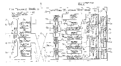
Fig.l is a circuit diagram showing the general arrangement
of a cell e~ch~nge apparatus 3 according to a first embodi-
ment of the present invention. The cell exchange apparatus
; ~
,, ~ .
.
:,.. .;
.:
2~1~73~
--6--
3 has input-stage cell exchange switch modules 60 to 63
which are provided to correspond to respective groups of
cell input ports 2 to exchange cells which are inputted to
the corresponding groups of input ports 2, output-stage cell
exchange switch modules 70 to 73 which exchange cells that
are delivered from cell exchange switch modules in the pre-
stage to specific output port groups, and cell output-stage
modules 80 to 83 which constitute final-stage modules.
Among the input-stage cell exchange switch modules 60
to 63, the module 60, for example, has an input-stage cell
multiplexing circuit 7 which subjects cells to time-division
multiplexing, and input-stage cell selecting circuits 8a
to 8d each of which selects and outputs through an address
filter a cell which is directed to a specific one of the
groups of output ports. Among the output-stage cell
exchange switch modules 70 to 73, for example, the switch
module 70, which is shown in Fig. 2, comprises the following
constituent elements: header processing circuits 9a to 9d
each of which reads and analyzes the destination information
of a cell that is outputted from the corresponding cell
selecting circuit in the pre-stage to a specific output port
group and then outputs the cell; memory circuits lOa to lOd
in which when write addresses are designated, cells that are
outputted from the header processing circuits 9a to 9d are
stored at the designated addresses, and when read addresses
are designated, the stored cells are read out irrespective
of the order in which they were written; an address exchange
circuit 16 which is provided in a memory control circuit 11
to distribute the addresses of cells that are written in the
memory circuits lOa to lOd into output port groups (herein-
after referred to as "outgoing lines") while referring to
the header processing circuits 9a to 9d; outgoing line
corresponding address FIF0 memories 17a to 17d which enables
distributed addresses to be written therein in correspon-
dence to outgoing lines and in the order of arrival; a readenable circuit 18 which gives a read address to each of the
memory circuits lOa to lOd at a predetermined timing to
enable reading of a stored cell; vacant address control
'
, ~: ':
. ~
2~19~39
--7--
circuits l9a to l9d which hold read addresses as vacant
addresses when cells are read out from the memory circuits
lOa to lOd and provide the addresses, as write addresses, to
new cells when arriving at the memory circuits lOa to lOd;
an output-stage cell multiplexing circuit 12 which multi-
plexes cells that are read out from the memory circuits lOa
to lOd; and output-stage cell selecting circuits 13a to 13d
which select and distribute through address filters cells in
the output signal from the circuit 12 which are directed to
specific ones of the groups of output ports. Among the cell
output-stage modules 80 to 83 shown in Fig. 1, the module
80, for example, has rate converting circuits 14a to 14d
which convert the rate of time-division multiplexed cells
into a rate of output ports.
The operation will next be explained. It is assumed
that in the arrangement shown in Fig. 1 cells have a fixed
length, and although input cells arrive at random, the input
phase of cells is adjusted before they are inputted to the
input ports I~ to Il 5 such that all cells which are inputted
from the input ports 2 are supplied in the same cell phase.
The operation of the input-stage (first-stage) cell
exchange switch modules 60 to 63 will first be explained
with reference to Fig. 5 which exemplarily shows the opera-
tion of the input-stage cell exchange switch module 60.
Cells in input signals A to D are subjected to time-division
multiplexing in the cell multiplexing circuit 7 to form a
signal E that is shown in Fig. 5. The signal E is delivered
to the input-stage cell selecting circuits 8a to 8d which
respectively correspond to the output ports o~ the input-
stage cell exchange switch module 60, in which the firstaddresses that are put to the header sections of cells
are detected to select and output cells which are to be
delivered to given output ports, as exemplarily shown by
signals F and P. Fig. 5 shows the way in which a cell, the
first address o-f which is "1", is outputted as a signal F,
while a cell, the -first address of which is "2", is out-
putted as a signal P. In this embodiment, multiplexing
is effected at a rate which is determined by multiplying
2019739
--8--
the link rate of input ports by the number of ports, for
example, with synchronized time slots each corresponding to
one cell, as shown in Fig. 5. A time slot which contains no
input cell is defined as a vacant slot, which is assigned a
first address that corresponds to none of the output ports.
Thus, in the input-stage cell exchan~e switch modules
60 to 63, cells which are inputted at the lin~ rate are
switched according to the first addresses that are put
to the respective header sections, and delivered to the
first-stage output ports in a burst manner at the rate of
multiplexing.
The operation of the output-stage (second-stage) cell
exchange switch modules 70 to 73 will next be explained with
reference to Fig. 2 which exemplarily shows the module 70.
Among the output signals from the input-stage cell exchange
switch modules 60 to 63, four signals that are inputted to
the output-stage cell exchange switch module 70 are assumed
to be F, G, H and I, respectively. The signals F to I
comprise cells which are delivered to the signals lines in
a burst matter at the speed of multiplexing and therefore
vary in the number of cells. Accordingly, these signals are
supplied to the memory circuits lOa to lOd for buffering,
which are provided to correspond to the input ports in the
output-stage cell exchange switch module 70. Thereafter,
the outputs of the memory circuits lOa to lOd are multi-
plexed in the output-stage cell multiplexing circuit 12.
It is considered that if input cells arrive uniformly both
temporally and spatially, all cells which are inputted
to the output-stage cell exchange switch module 70 can be
multiplexed without being wasted on condition that the rate
of the output signal J from the output-stage cell multiplex-
ing circuit 12 is not lower than a rate which is determined
by multiplying the input link rate of the output-stage cell
exchange switch module 70 by the number of ports. In actual
practice, however, the arrival of cells varies both tempo-
rally and spatially and it is therefore necessarY to buffer
cells in the memory circuits lOa to lOd to thereby absorb
overflow of cells.
,
- : , :.
201 9739
g
The memory control circuit 11 has a function to
prevent successively reading cells which are addressed to
the same outgoing line and also prevent inversion of the
order in which cells are read out. More specifically, when
cells are stored in the memory circuits lOa to lOd, the
addresses of the cells in the memory circuits lOa to lOd
are distributed into outgoing lines by the address exchange
circuit 16 and these addresses are then stored in the outgo-
ing line corresponding address FIFO memories 17a to 17d in
order to control and store the addresses of the cells in the
memory circuits lOa to lOd in correspondence to the outgoing
lines. The read enable circuit 18 refers to the outputs of
the FIFO memories 17a to 17d and gives read addresses to all
the memory circuits lOa to lOd to send out cells therefrom
within the range in which the output-stage (post-stage)
cell multiplexing circuit 12 is capable of multiplexing the
outputs of all the memory circuits lOa to lOd. A variety of
methods may be considered usable to c.ontrol reading from the
memory circuits lOa to lOd, for example, a method wherein N
(an integer not less than 2) cells are read out in succes-
sion with respect to an outgoing line for which the amount .
of cells being held in the FIFO memories 17a to 17d is
greater than a predetermined value, while n (1 or 0) cell
is read out with respect to other outgoing lines, thereby
effectin~ multiplexing; and a method wherein the amounts
of cells which are addressed to various outgoing lines
are compared with each other, and N cells are read out in
succession with respect to an outgoing line for which the
amount of cells being held is the largest, while n cell is
read out with respect to other outgoing lines, for multi-
plexing purpose. In either method, a larger number of cells
are read out for an outgoing line to which are addressed a
relatively large number of cells than for an outgoing line
to which are addressed a relatively small number of cells.
Under these circumstances, the reading for an outgoing line
to which are addressed a relatively small number of cells
may be suspended and the delay time may exceed a predeter-
mined value. Any method which may give rise to such a
2 ~
--10--
problem must not be used. In the output-stage (final-stage)
cell exchange switch module 70, reading from the memory
circuits lOa to lOd must be executed uniformlY in order to
prevent overElow in the post-stage of the outgoing lines
where rate conversion is needed. Accordingly, the read
enable circuit 18 in the output-stage (final-stage) cell
exchange switch module 70 effects control such that cells
which are addressed to respective outgoing lines are read
out in the numerical order of the outgoing lines.
The following is a description of the operation of an
output-stage cell exchange switch module 70, as one example,
which is not one in the final stage but in an intermediate
stage that is followed by another output-stage cell exchange
switch module. The description will be made with reference
to the timing charts of Figs. 5 and 6, in regard to a multi-
plexing method wherein two cells are read out in succession
with respect to an outgoing line for which the number of
cells being held exceeds 4 (equivalent to the number of
input ports), while 1 or 0 cell is read out with respect
to an outgoing line for which said number is not greater
than 4.
It is assumed that cell strings such as those shown
in Fig. 6 are inputted as signals F to I. The signal G
shows that a series of nine cells is delivered from the
input-sta~e cell exchange switch module 61 to outgoing lines
K, L, M and N. The FIF0 memories 17a, 17b, 17c and 17d
correspond to the out~oing lines K, L, M and N, respec-
tively. The read enable circuit 18 monitors the amount of
cells being held in each of the FIFO memories 17a to 17d.
First, at the time when the address at which a first cell is
stored is stored in any of the FIF0 memories 17a to 17d, the
read gate of the FIF0 memory 17a corresponding to the outgo-
ing line K is opened to fetch an address. Then, one cell
that corresponds to the fetched address is outputted from
the memory circuit lOa to the output-stage cell multiplexing
circuit 12 to start multiplexing. Multiplexing is effected
in units of cells through the FIF0 memories 17a, 17b, 17c
and 17d in the mentioned order. If no cell is stored in
.
~9733
an FIFO memory, the process immediately shifts to the next
FIFO memory to continue the multiplexing. In this example,
the first cell is a first cell in the signal F, which is
directed to the outgoing line K (each cell being hereinafter
denoted by a number, e.g., Fl, that is put to the data sec-
tion of the cell). Accordingly, an address is first fetched
from the FIFO memory 17a and this address is given as a read
address to the memory circuit lOa to read out and multiplex
the corresponding cell. At the same time, the read address
is supplied to the vacant ad~ress control circuit 191a.
Upon completion of the multiplexing of the readout cell, an
address is fetched from the FIFO memory 17b corresponding
to the outgoing line L to multiplex the cell G2. Next, an
address would otherwise be fetched from the FIF0 memory 17c
corresponding to the outgoing line M, but the FIFO memory
17c is vacant and consequently the process immediately
shifts to the FIFO memory 17d corresponding to the outgoing
line N. Thus, an address is fetched therefrom! and the cell
G3 is multiplexed. Next, the cell Gl that is addressed to
the outgoing line K is multiplexed, followed by the cell I1
to the outgoing line L, the cell G6 to the outgoing line M,
and the cell G7 to the outgoing line N. The process then
proceeds to the FIF0 memory 17a corresponding to the
outgoing line K. Since the number of cells being held in
the FIFO memory 17a at this time is 5 (indicated by o in
Fig. 4), two addresses are successively read out therefrom.
Thus, the cells H1 and G4 are multiplexed. Thereafter, the
cells H2, H3, G5, G9, F3, H5, F2, H4, I2, G8, F4 and G10 are
multiplxed in the mentioned order.
Thus, by virtue of the FIF0 memories 17a to 17b
in the output-stage cell exchange switch module 70, it is
possible to control the addresses in the memory circuits lOa
to lOd and cells can be temporarily stored therein. In
general, the sum total of cells which are supplied to the
output-stage cell exchange switch modules 70 to 73 from the
signal lines corresponds, on the average, to a rate which is
determined by multiplying the input link rate by the number
of input ports as long as there is neither temporal nor
. ,- - . .
. .
",
.-. : .: , :
.~ , " : .: . :,
-:
~ 2019739
-12-
spatial deviation, and it is therefore considered to be
equal to or less than the total number of cells which can
be multiplexed on multiplex signals that are produced in the
output-stage cell exchange switch modules 70 to 73. Since
a variation in the number of cells being held in the memory
circuits 10a to 10d is caused by the fact that the number of
cells arriving varies from an average both temporally and
spatially, it is possible to absorb a temporal variation and
minimize the waste of cells by temporarily storing cells in
the memory circuits lOa to lOd, as described above.
In addition, the memory circuits lOa to lOd in the
output-stage cell exchange switch modules 70 to 73 are
capable of writing at a high rate of multiplexing and also
capable of reading at the link rate of the outgoing lines
15' even if a plurality of cells arrive simultaneously. Accord-
ingly, even if a plurality of cells are concentrated at the
same time, no cell is wasted as long as the number of cells
concentrated is within the capacity of the memory circuits
lOa to lO~.
Although in the foregoing embodiment the respective
numbers of input and output ports in the whole cell exchange
switch are the same, the numbers of input and output ports
may be different from each other. The number of stages of
,
the output-stage cell exchange switch modules 70 to 73 may
also be increased as desired. Although in the ~oregoing
embodiment the numbers of input and output ports in the
whole cell exchange switch are each 16 and each cell
~; ~ exchange switch module has 4 input ports and 4 output ports,
these numbers may be changed as desired. In addition, the
cell exchange apparatus of the present invention is not
necessarily divided into modules such as those described
above but may be fabricated in the form of a single cell
; exchange switch.
In the foregoing embodiment, the number of an outgo-
3S ing line is put to the header section of a cell for each of
the two address sections for two groups of cell exchange
switch modules which are provided in two stages. However,
the number of an outgoing line may be represented by another
.~ :
~: :
., - : ~ ~ ; ," ,
,: : : - ~ .. : , . .
,,, :
2~ 9~3~
-13-
form, for example, a coded number which is put to a single
address section of a cell.
Although in the foregoing embodiment one cell is
outputted to only one output port, it is possible to set the
output-stage cell selecting circuits 13a to 13h so as to
output one cell to a pluralitY of output ports by properly
arranging the way of addressing. Thus, a broadcasting
function may be added to the arrangement described above.
The arrangement may also be such that the header
and data sections of cells are separated from each other
and these sections are assigned to a plurality of signal
lines, which are arranged in parallel, by use of respective
circuits which have different rates of transmiss~on.
Although in the foregoing embodiment the link rate of
the input ports is the same as the output port rate, if the
rate of reading from the output-stage memory circuits lOa
to lOd, shown in Fig. 1, is made higher than the input port
link rate, traffic concentration can be achieved, and it is
also possible to make the input port link rate higher than
the output port rate. In addition, although the multiplex-
ing rate of the signal J is the same as that of the signal
E, if the multiplexing rate of the signal J is made higher,
it is possible to further reduce the rate at which cells are
wasted in transmission between cell exchange switch module
stages.
Although in the foregoing embodiment the FIFO
memories 17a to 17d are provided to correspond to the outgo-
; ing Iines, respectively, of the output-stage cell exchange
switch module 70, it is also possible to provide a plurality
of FIFO memories for each outgoing line according to the
order of priority so that a cell of higher priority is first
multiplexed on the basis of a sign representative of a level
of priority that is added to the header section of a cell in
addition to an address. Although the read enable circuit 18
is arranged such that when the number of cells being held in
any one of the FIFO memories 17a to 17d exceeds 4, two cells
are successively read out therefrom, it should be noted that
the number is not necessarily limitative to 4 and that any
~- :, :. :: . .
- . ~
2~739
-14-
other numerical value may be employed. The present inven-
tion may be applied to any system wherein reading from an
FIFO memory which has a relatively large number of cells
being held therein is preferentially executed.
When the operating speed must be limited, a serial-
to-parallel converter circuit and a parallel-to-serial
converter circuit may be added to the input and output ends,
respectively, of this switch to process data in the form
of parallel signals.
As has been described above, the cell exchange
apparatus according to the first embodiment of the present
invention is arranged such that input cells are multiplexed
in an input-stage cell exchange switch module before being
distributed, and in an output-stage cell exchange switch
lS module a cell string which is inputted from a pre-stage
cell exchange switch module is stored in memory circuits
and the cells in the memory circuits are read out according
to a predetermined output rule by a memory control circuit.
Accordingly, even if cells are concentrated in a specific
output port group at the same time, no cell is wasted as
long as the number of cells concentrated is within the
capacity of the output-stage memory circuits.
A second embodiment of the pre.sent invention will
next be explained with reference to Figs. 3 and 4. In
Fig. 3, the same reference numerals as those shown in Fig. 1
denote the same elements, and in Fig. 4, the same reference
numerals as those shown in Fig. 2 denote the same elements.
As will be understood from the figures, the second embodi-
ment is the same as the first embodiment in regard to the
arrangements of many portions; therefore, description of the
same portions is omitted to prevent complication.
In Figs. 3 and 4, reference numeral 4 denotes space
switches that operate in such a manner that cells, which are
outputted from the input-stage cell selecting circuits in
the input-stage cell exchange switch modules 60 to 63 to
specific output port groups, are preferentially stored in
memory means (memory circuits; described later) lOa to lOd
~ (lOe to lOh) which have a relatively small amount of cells
:~
...-!
~ - '; ; , ' ' ~
', . : ' : :
,
: ' . :
:, ': . . : ' '
,, ,:
:: ' ':
2 ~ 7 ~ ~
-15-
being held therein, in order to make uniform the amount of
cells being held among the memory circuits lOa to lOd (lOe
to lOh).
Referring to Fig. 4, reference numeral 15 that is
shown in the memory control circuit 11 denotes a memory
circuit counter which controls the amount of cells being
held in each of the memory circuits lOa to lOd.
The operation will next be explained. Since the
arrival of cells which are inputted to the output-stage
cell exchange switch module 70 varies both temporally and
spatially, it is necessary to buffer cells in the memory
circuits lOa to lOd to thereby absorb overflow of cells.
The space switch 4 refers to the counter 15 for the amount
of cells being held in each of the memory circuits lOa to
lOd and stores each input cell preferentially in a memory
circuit which has a relatively small amount of cells being
held therein, thereby making the amount of cells being held
as uniform as possible among the memory circuits lOa to lOd.
More specifically, the space switch 4 refers to the memory
circuit counter 15 in the memory control circuit 11 and,
when m cells arrive at the same time, the space switch 4
selects from among the memory circuits lOa to lOd m memory
circuits, from one which has the smallest amount of cells
being held therein, and successively writes the cells in the
selected memory circuits, respectively.
At this time, the cells that a.re outputted from the
space switch 4 are delivered to given memory circuits lOa to
lOd through the corresponding header processing circuits 9a
to 9d, which analyze the destinations of the cells concerned
and deliver the identification information of the corre-
sponding ones of outgoing lines K to N to the address
exchange circuit 16 in the memory control circuit ll. When
the cells are stored in the memory circuits lOa to lOd, the
addresses where the cells are stored are delivered to the
address exchange circuit 16 by the corresponding vacant
address control circuits l9a to l9d. The address exchange
circuit 16 stores the delivered addresses in the FIFO
memories 17a to 17d corresponding to the outgoing lines K
~'
.
.. ..
: .
~g~
-16-
to N which are designated by the header processing circuits
9a to 9d. At this time, the memory circuit counter 15
counts and controls the amount of cells being held in each
of the memory circuits lOa to lOd.
In comparison to the first embodiment, the above-
described second embodiment provides the following advan-
tages: Since the space switch ~ is emploYed to preferen-
tially write cells in memory circuits lOa to lOd (lOe to
~Oh) which have a relatively small amount of cells being
held therein in order to make the amount of cells being held
as uniform as possible among the memory circuits lOa to lOd
(lOe to lOh), the memory circuits lOa to lOd (lOe to lOh)
can perform in substantially the same way as in the case of
a single relatively large memory circuit which is mutually
used for all the incoming lines. It is therefore possible
to further reduce the rate at which cells are wasted due to
the fact that the arrival of cells varies both temporally
and spatially.
Thus, according to the second embodiment of the
present invention, when receiving cells which have been once
multiplxed and distributed into destinations in the input-
stage cell exchange switch module, the output-stage cell
exchange switch module preferentially writes the cells into
memory means which ha~Te a relatively small amount of cells
being held therein, and the cells are read out from the
memory means under the control of the memory control means
and multiplexed again for each destination before being
distributed to the corresponding output ports. Accordingly,
it is possible to obtain a cell exchange apparatus which
is free from the problem of blocking and in which, even if
cells are concentrated in a specific output port, there
is little probability that the cells will be wasted, and
switching can be performed without affecting cells which
are directed to other output ports.
.,' ' :
.. ..