Note: Descriptions are shown in the official language in which they were submitted.
2 ~ ~ ~ 7 ~ 3
SHARPNESS UP/DOWN CIRCUIT FOR VCR CONTROLLED BY A
REMOTE CONTROLLER AND CONTROL METHOD THEREOF
The present invention relates to a sharpness control
circuit for a video cassette tape recorder (hereinafter
referred to as a VCR). More particularly the invention
relates to a sharpness up/down circuit controlled by a
remote controller, and a control method thereof which
enables remote control of the sharpness of a picture
generated by VCR by manipulating a remote controller.
For the conventional VCR sharpness is controlled by
manually manipulating a variable sharpness key or input.
The key is mounted on a keyboard. Control of sharpness
by a remote controller is not used. Therefore, a user
has to manipulate the variable sharpness directly, and
manually, on the playback of VCR.
The present invention seeks to provide a VCR
sharpness up/down circuit, and a control method thereof,
which allow remote control of sharpness of the VCR by
pressing a sharpness-up key or a sharpness-down key on a
remote controller.
In the first aspect the invention is a sharpness
up/down circuit for a video cassette tape recorder
controlled by a remote controller, comprising:
a remote controller for generating remote
control signals such as sharpness up/down key
signals;
a microcomputer for counting a number of times
said sharpness up/down key signals are received from
said remote controller and for selecting and
outputting a pulse width modulation signal according
to the number of times counted;
sharpness driving means for converting said
pulse width modulation signal outputted from said
microcomputer to a direct current voltage through
~ 20~7~3
switching operations and for outputting said pulse
width modulation signal as a sharpness driving
voltage; and
screen control means for controlling sharpness
of the video cassette tape recorder by varying
emphasis on high frequency components of video
signals according to a magnitude of said sharpness
driving voltage outputted from said sharpness
driving means.
In a second aspect the invention is a method for
controlling a sharpness up/down for a video cassette tape
recorder by a remote controller, comprising the steps of:
(a) setting a count value for an output pulse
width modulation counter as a sharpness center value
when power is supplied;
(b) selecting an address of a pulse width
modulation data storage unit according to the count
value of the pulse output width modulation counter
in a playback mode;
(c) reading pulse width modulation data stored
at the address and outputting the data to the pulse
output width modulation counter;
(d) increasing or decreasing the count value
of the pulse output width modulation counter by one
until the count value of the pulse output width
modulation counter reaches a highest or lowest level
when a sharpness-up or a sharpness-down key signals
is inputted; and
(e) selecting the pulse width modulation data
and outputting the data according to the count
value.
In the drawinqs:
Fig. 1 is a block diagram showing a sharpness
up/down circuit controlled by a remote controller
according to the present invention,
7 ~ 3
Fig. 2 is a detailed circuit diagram showing a
sharpness driving unit of Fig. 1,
Fig. 3 is a detailed block diagram for a screen
control unit of Fig. 1,
Figs. 4A through 4D are pulse width modulation
signal output waveforms of Fig. 2,
Fig. 5 is a view showing characteristics of
sharpness output voltage according to pulse width
modulation signal of Fig. 4,
Figs. 6A through 6E are waveforms from each part of
Fig. 3, and
Fig. 7 is a flowchart for sharpness up/down
controlled by a remote controller according to the
present invention.
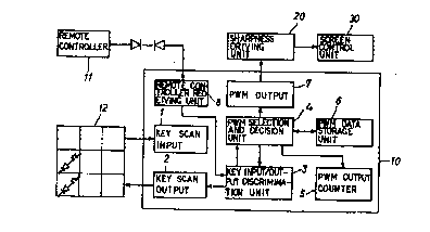
As shown in Fig. 1, the present invention consists
of a remote controller 11 which generates remote-control
signals, for example, sharpness up/down key signals, etc.
There is a key matrix 12 for selecting various function
keys. A microcomputer 10, selects and outputs a
corresponding pulse width modulation (PWM) signal when
the sharpness up-down key signal input exists. The
microcomputer 10 first checks a key selection status with
a scan of said key matrix 12 as well as reception of said
remote control signal from the remote controller 11. A
sharpness driving device 20 converts the PWM signals
outputted from said microcomputer 10 to a DC voltage and
outputs it as a sharpness driving voltage. A screen
control unit 30 varies the screen sharpness according to
the magnitude of the sharpness driving voltage outputted
from the sharpness driving unit 20.
Microcomputer 10 includes a key scan input device 1
and a key scan input device 2 that scan the key matrix
12. A remote control receiving unit 8 receives the
remote control signal of the remote controller 11. A key
input/output discrimination unit 3 discriminates a key
signal input to the key scan input unit 1 and a key
7 ~ 3
signal of a remote control signal received at said remote
control receiving unit 8. A PWM selection/decision unit
4 selects and outputs PWM data from a PWM data storage
unit 6 according to the counted number of a PWM output
counter unit 5 with a sharpness up/down key
discrimination signal of the key input/output
discrimination 3. A PWM output unit 7 outputs a PWM
signal according to the PWM data outputted from the PWM
selection/decision unit 4.
As shown in Fig. 2, the sharpness driving unit 20
has a power supply unit 21 which supplies through ripple
eliminating capacitors C1 and C2, a resistor R1 and a
diode D1 a rated DC power drawn out by a zener diode ZD1
after power of a power terminal Vcc passes through a coil
Ll. A PWM input surge elimination unit 22 eliminates
surge. The output PWM signal from the PWM output unit 7
is passed through a resistor R5 and a capacitor C7. A
switch 23 performs a switching control of output of the
power supply unit 21 with control of a transistor Q1
driven by a PWM signal through said PWM input surge
elimination unit 22 wherein a bias resistor R6 and a high
frequency elimination coil L2 are connected respectively
to the base and to the collector of the transistor Q1.
An integrator 24 outputs, as a sharpness driving voltage,
the output of the power supply unit 21 on which a third
integration is performed through capacitors C3-C6 and
resistors R2-R4, j oined in parallel. As shown in Fig. 3,
the screen control unit means 30 comprises an emphasis
integrator 32 that performs a variable emphasis on high
frequency components of video signals outputted from the
video signal input unit 31 according to the sharpness
driving voltage outputted from the sharpness driving unit
20. A high-pass filter 33 allows only high frequency
signal to pass through it. The signals are the output
signals of the integrator 33. A limiter 34 limits the
amplitude of the signals outputted from the high-pass
filter 33. A mixer mixes the output signals of the
a 2 0 1 ~ 7 1~ 3
limited 34 with the output signals of the video signal
input unit 31. A clamp 36 sets the output signal level
of the mixer 35 at a certain level.
Figs. 4A through 4C are illustrative views showing
waveforms of the PWM output unit 7 in Fig. 2, and Fig. 4D
illustrates the integration process of the integrator 24
in Fig. 2.
Fig. 5 illustrates the output voltage of the
integrator 24 according to Figs. 4A to 4C.
Fig. 6A to 6E are waveforms for each part of Fig. 3.
Fig. 7 is a control flowchart of the microcomputer
10 of Fig. 1.
Use of the present invention is as follows:
First, referring to Fig. 7, a count value of the PWM
output counter unit 5 becomes a sharpness centre count
value at the PWM selection/decision unit 4 when power is
supplied by the power key.
Thereafter, when in the tape playback mode, an
address of the PWM data storage unit 6 is selected by the
count value of the PWM output counter unit 6, that is, by
the medium count value. The PWM data stored at the
address are read by the PWM selection/decision unit 4 and
outputted through the PWM output unit 7. In such a
state, when the sharpness key signal is inputted to the
key input/output discrimination unit 3 through key scan
input unit 1 of the remote control receiving means 8, it
is determined whether the sharpness key signal is a down
key signal or an up key signal.
If a sharpness down key signal exists, the count
value of the PWM output counter unit 5 decreases by "1"
at the PWM selection/decision unit 4, and the address of
the PWM data storage unit 6 is selected by the count
value of the PWM output counter unit 5. The PWM data
stored at the location of the address are read at the PWM
selection/decision unit 4 and outputted through the PWM
output unit 7.
A
7 ~ 3
If a sharpness-up key signal exists, the count value
of the PWM output counter unit 5 increases by "1" at the
PWM selection/decision unit 4, and the address of the PWM
data storage unit 6 is selected by the count value of the
PWM output counter unit 5. PWM data stored at the
location of the address are read at the PWM
selection/decision unit 4 and outputted through the PWM
unit 7.
The above process is performed repeatedly every time
the sharpness key signal is inputted. The status that
continues to output the lowest PWM data at the PWM
selection/decision unit 4 is maintained because another
input of the sharpness-down key signal does not decrease
the count value of the PWM output counter unit 5 when the
PWM data outputted at the PWM selection/decision unit 4
is at its lowest. Likewise, the highest PWM data
continue to be outputted at the PWM selection/decision
unit 4 because another input of the sharpness-up key
signal does not increase the count value of the PWM
output counter unit 5 when the PWM data outputted at said
PWM selection/decision unit 4 is at its highest.
As mentioned above, the PWM signal outputted from
the PWM output unit 7, after the surge is eliminated by
the PWM input surge elimination unit 22 of the sharpness
driving unit 20, acts to turn the transistor Ql of the
switching unit 23 on/off.
Power at the power supply terminal Vcc is converted
to a rated direct current source through coil Ll by zener
diode ZDl. Ripple components of the direct current
source are eliminated by ripple-eliminating capacitors Cl
and C2 and applied to the collector of the transistor Ql
through a resistor Rl and a diode Dl. Accordingly, the
signal of waveform (c) shown in Fig. 4D is outputted at
the collector because on/off repetition of the transistor
Ql is made according to the rectangular wave signal (a)
of a certain period as shown in Fig. 4D. The signal is
applied to the transistor Ql of the switching means 23
A
~ 2 ~ ~ 9 7 ~ 3
through the PWM input surge elimination means 22. At
this time, spike phenomena (dotted circles) of high
frequency components as shown in Fig. 4D are eliminated
by coil L2 connected to the emitter of the transistor Q1.
The output waveform signal to which the third
integration is applied at the integrator 24, as shown in
the waveform of Fig. 4d, is outputted as a sharpness
driving voltage P1 of a certain DC voltage. At this
time, the waveform signal (c), to which the first
integration is applied through a resistor R2 and a
capacitor C4, is converted to the level (d), converted to
the level (e) after a second integration through a
resistor R3 and a capacitor C5, and outputted as a
sharpness driving voltage P1 of a certain DC voltage
after a third integration through a resistor R4 and a
capacitor C6.
Accordingly, the level of the sharpness driving
voltage P1 outputted from the integrator 24 becomes
minimum (MIN) as shown in Fig. 5 because the turn-on time
of the transistor Q1 grows longer and its turn-off time
grows shorter when the PWM signal of a certain period T
outputted from the PWM output means 7 becomes minimum as
shown in Fig. 4A. That is, the high potential section
becomes longer and the low potential section becomes
shorter during a certain period T.
The level of the sharpness driving voltage P1
outputted from the integrator 24 becomes intermediate
(CEN) as shown in Fig. 5 because the turn-on time and the
turn-off time of the transistor Q1 are substantially the
same when the PWM signal of a certain period T outputted
from the PWM output unit 7 is intermediate as shown in
Fig. 4B.
The level of the sharpness driving voltage P1
outputted from the integrator 24 becomes maximum (MAX) as
shown in Fig. 5 because the turn-on time of the
transistor Q1 goes shorter and the turn-off time goes
longer when the PWM signal of a certain period T
A
outputted from the PWM output unit 7 is maximum as shown
in Fig. 4C.
As mentioned above, application of the sharpness
driving voltage P1 outputted from the sharpness driving
5 unit 20 to an emphasis integrator 32 as a control voltage
makes a variable emphasis on high frequency components of
the video signal. Thus, the high frequency components of
the video signals are emphasized, as shown in Fig. 6B,
according to the magnitude of the sharpness driving
voltage P1 at the emphasis integrator 32 when the video
signals as shown in Fig. 6A are outputted from the video
signal input means 31.
When the sharpness driving voltage P1 is high, the
high frequency components of the video signals are
15 greatly emphasized. When the level of the sharpness
driving voltage P1 is low, the high frequency components
of the video signals are slightly emphasized. As
described above, the high frequency component signals
pass through the high-pass filter 33 as shown in Fig. 6C.
20 The amplitude of the components is limited through the
limiter 34 as shown in Fig. 6D. The output signals of
the limiter 34 are applied to the mixer 35 and mixed with
the video signals as shown in Fig. 6A. The mixed signals
are applied to the clamp means 36 for clamping to a
25 certain level as shown in Fig. 6B. Thus, the sharpness
of the screen is controlled. Consequently, the sharpness
of the video signals is controlled by performing a
variable emphasis on the high frequency components of the
video signals at the emphasis integrator 32 according to
30 the level of the sharpness driving voltage P1 from the
integrator 24.
The present invention therefore provides a user with
more convenience because pressing the sharpness up/down
keys on the remote controller performs a variable
35 emphasis on the high frequency components of the video
signals and provides automatic sharpness control.