Note: Descriptions are shown in the official language in which they were submitted.
ELECTRIC DOUBLE LAYER CAPACITOR
BACKGROUND OF THE INVENTION
The present invention relates to an electric double layer
capacitor of high electrostatic capacitance which utilizes the
principles of an electric double layer that is composed of an
interface between activated carbon and electrolyte.
Recently, high capacitance capacitors based on the electric
double layer principles have been developed as backup power
supplies for memories in electronic systems, and are widely used
with microcomputers and IC memories.
one type of electric double layer capacitor is disclosed in
U.S. Patent 3,536,g36, for example.
It is important that the internal resistance of an electric
double layer capacitor be low. The internal resistance of an
electric double layer capacitor is greatly affected by the
contact resistance of active carbon of the polarized electrodes
and the contact resistance between the collector electrodes and
the
.. ..
:
- l -
'i
... ; . . ... . . : . . ..
-: . , - , . -. . . ~ .. : - . -
: . . , , ~ - , .. - ... ~ . .. . .
Therefore, in order to reduce the internal resistance of the
polarized electrodes and the contact resistance between the
collector and polarized electrodes, each basic cell should be
kept under vertical pressure to bring the particles of the paste
activated carbon into good electric contact with each other.
Conventional electric double layer capacitors require each cell
to be kept under a pressure of about 100 kg/cm2 though it depends
on the size of the electrodes, the ~ize of the particles of the
carbon material, or the kind of the electrolyte used. In prior
electric double layer capacitors, the cells are kept under
pressure by deforming the outer cases of the capacitors or
bonding the current collectors strongly to gaskets. If an
electric double layer capacitor is to be used as a large-
capacitance capacitor, e.g., a power supply for energizing amotor, then it is necessary to increase the cross-sectional areas
of the electrodes of the ba5ic cell. Therefore, the
.
-- 2 --
. ~,
, , : . , . , - . . ~ . : :
2020~47
pressure to be applied to the basic cell has to be
increased. Increasing the pressure, however, causes some
practical problems such as the selection of means for apply-
ing the pressure and the ~eed for high rigidity for the
outer cell which houses the basic cell.
SUMMARY OF THE INVENTION
It is an object of the present invention to provide
an electric double layer capacitor havlng an electric double
layer composed of an interface between activated carbon and
electrolyte, the electric double layer capacitor having a
simple construction, a hlgh energy density, and requiring no
means for pressurizlng electrodes.
Another ob~ect of the present invention is to pro-
vide a method of easily manufacturing polarized electrodes
for use in an electric double layer capacltor.
According to the present invention, there is pro-
vided an electrlc double layer capacitor having an electric
double layer composed of an interface between activated car-
bon and electrolyte, comprlslng at least two polarized elec-
i trodes each comprlsing a porous slntered body which conslsts
of slntered and ~olned flne partlcles of activated carbon, a
separator lnterposed between the polarized electrodes, and a
casing in which the polarized electrodes, the separator, and
; an electrolyte are sealingly accommodated.
According to the present invention, there is also -
provided an electric double layer capacitor having an elec-
. ,
-- 3 --
2020~47
tric double layer composed of an interface between activated
carbon and electrolyte, comprising at least two polarized
electrodes each comprising a porous sintered body which con-
sists of sintered and joined fine particles of activated
carbon, the polarized electrodes being impregnated with an
electrolyte, two current collectors thermally fused to one
surface of the polarized electrodes, respectively, the cur- :
rent collectors being made of an electrically conductive
material, a separator interposed between the polarized elec-
trodes and impregnated with an electrolyte, and a gasket
disposed between the current collectors in surrounding rela-
tlon to the polarized electrodes and the separator, the gas-
ket being attached to the current collectors.
According to the present invention, there is fur-
ther provided a method of manufacturing a polarized elec-
trode for an electrlc double layer capacitor having an
electrlc double layer composed of an interface between acti-
vated carbon and electrolyte, the method comprlslng the
steps of applylng a pressure ranglng from 50 Kgf/cm~ to 800
Kgf/cm~ to a powder of fine partlcles of activated carbon
placed in a mold, and while the pressure is being applied to
the flne particles, applying pulse voltages between the fine
partlcles for producing electric discharges between the fine
partlcles, and keeping the fine particles at a temperature
ranging from 700C to 1000C, thereby sintering the fine
particles of activated carbon.
, i ,
~ .
2020~47
The above and other objects, features and advan-
tages of the present invention will become more apparent
from the following description when taken in conjunction
with the accompanying drawings in which preferred embodi-
ments of the present invention are shown by way of illustra-
tive example.
BRIEF DESCRIPTION OF THE DRAWINGS
Fig. 1 is a dlagram showing a model for manufact-
uring a porous sintered body which constitutes a polarized
electrode in an electric double layer capacitor according to
the present inventlon;
Fig. 2 is a graph showing the pressure applied to
fine partlcles of activated carbon, the average current
flowing through the fine particles, and the temperature of
the fine partlcles, as they change wlth time;
Fig. 3 is a cross-sectlonal view of a porous sin-
tered body which is formed by a process according to the
present invention;
Fig. 4 ls a dlagram lllustrating a region in which
fine particles of activated carbon can be slntered into a
porous body;
Flg. 5 is a circult dlagram showlng an apparatus
for manufacturlng a porous slntered body accordlng to the
present lnvention;
Flg. 6 ls a timlng chart showing a discharged
. .
condltion;
:
~ 5 ~
..
- : ~ : :-
Fig. 7 is a table showing performances of an electric double
layer capacitor according to Inventive Example 1 and an electric
double layer capacitor according to Comparative Example;
Fig. 8 is a graph showing the relationship between the
pressures applied to the electrodes of the electric double layer
capacitors according to Inventive Example 1 and Comparative
Example and the internal resistances of these electric double
layer capacitors;
Fig. 9 is a cross-sectional view of an electric double layer
capacitor according to Inventive Example 2:
Fig. 10 is a cross-sectional view of a stacked electric
double layer capacitor; and
Fig. 11 is a cross-sectional view of a conventional electric
double layer capacitor which has paste electrodes of a slurry.
DETAILED DESCRIPTION OF THE PREFERRED EMBODIMENTS
Prior to describing preferred embodiments of the present
invention reference will initially be made to fig. 11 which
illustrates a conventional electric double layer capacitor.
Fig. 11 of the accompanying drawings shows the structure of
the electric double layer capacitor disclosed in U.S. Patent
3,536,936. The electric double layer capacitor comprises a
single basic cell composed of a pair of current collectors 101
of an electron conductor which serves as a pair of collector
eleatrodes, a pair of carbon electrodes 102 made of activated
-- 6 --
......
p~.
...... . .. ..
: - , .. . .~ - . - , - - : :
- , . - - - , .
carbon particles, a pair of non-conductive gaskets 103, and an
isolating plate 104 positioned between the carbon electrodes 102
for preventing electrons from moving between the electrodes 102.
The carbon electrodes 102 are made as paste electrod~s from a
concentrated slurry which is a mixture of powdery or particulate
activated carbon and an electrolyte. The electrolyte has three
functions to perform. It serves as a promoter of ion
conductivity, an ion source, and a binder for the carbon
particles.
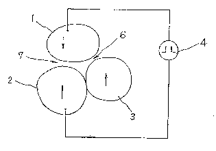
Fig. 1 schematically shows a model for manufacturing a
polarized electrode for use in an electric double layer capacitor
according to the present invention. In Fig. 1, the reference
numeral 1 denotes a fine particulate of activated carbon and the
reference numerals 2, 3 also denote fine particles of activated
carbon. The fine particle 3 is joined to the fine particle 2.
A pulse power supply 4 generates a sharp pulse voltage.
When an instantaneous pulse voltage i8 applied between the
fine particle 1 and the fine particles 2, 3 by
- 6a -
:
. ~ . .
; -
,
'
., .
.. , .. .. ~.
. . .
:~: ., ., -, . . .
2020~47
the pulse power supply 4, the electric field across gaps 6, 7
between the fine particles is built up in intensity. As the
intensity of the electric field exceeds a predetermined
voltage, a dielectric breakdown occurs between the fine par-
ticle 1 and the fine particles 2, 3, producing a spark dis-
charge across the gaps 6, 7. At this time, electrons
emitted from the fine particles 2, 3 and ion bombardment on
the fine particle 1 sufficiently purify the surfaces of the
fine particles. The spark discharge produces a large pres-
sure between the electrically conductive fine particles, the
impulse pressure due to the spark discharge imparts distor-
tion to the fine particles of activated carbon. Joule heat
generated by a subsequently flowing current spreads from
points where the fine partlcles are close to each other,
making the activated carbon particles plastically deformable
easily. Since the pressure is imposed between the fine par-
ticle 1 and the fine particles 2, 3 in the directions
indicated by the arrows, the particles 1 and 2, 3 are moved
toward each other, and brought lnto contact through small
points. Carbon atoms of the partlcles are therefore
efflclently diffused and moved through these polnts of
contact.
Flrst, small plastic deformation takes place on the
fine partlcles, and the fine particles move toward each
other until finally they are brought into point-to-point
contact with each other. The areas through which the fine
- 7 -
.
-.: . ~ , . : -
... .. ' ~ .
2020547
particles contact each other are progressively spread.
Consequently, more and more fine particles are packed into a
space having a unit volume. AS the areas through which the
fine particles contact each other are spread, the contact
resistance therebetween are greatly reduced, and so is the
amount of heat generated. Therefore, the contacting regions
of the fine particles are cooled, and melted portions
thereof are solidified and the fine particles are firmly
bonded to each other.
The above process ls not continuously carried out
at once. More specifically, the duratlon of a pulse voltage
applied between flne partlcles is very short, and hence the
application of a pulse voltage is interrupted while the fine
particles are moving toward each other. Therefore, the
spark discharge produced across the gaps 6, 7 between the
fine particles ls also lnterrupted. The generation of heat
is also interrupted, and the temperature near the gaps is
not increased until the flne particles collapse, and ls kept
below the recrystallization temperature at all times. When
a next pulse voltage ls applled across the gaps 6, 7, the
above actlon occurs again. The dlscharge of the above
nature is repeated until the flne particles 1 and 2, 3 are
brought lnto contact and bonded to each other. The repeated
application of pulse voltages causes the fine particles to
be sufflciently ~oined to each other, resulting in a porous
sintered body which is composed of only activated carbon.
-- 8
. . .
2~20547
Fig. 2 illustrates the pressure applied to fine
particles of activated carbon, the average current flowing
through the fine particles, and the temperature of the fine
particles, as they change with time.
If only a DC voltage were applied between fine par-
ticles of activated carbon, the spark discharge would con-
tinue for a long period of time untll the fine particles are
brought into contact with each other, and the spark dis-
charge would develop into an arc discharge, with the result
that the temperature ln the vicinity of the gaps 6, 7 would
rise to the degree that the fine particles would be melted
entlrely. Therefore, the fine particles would be melted and
collapse away into a large mass of carbon, and no porous
sintered body would be formed.
Fig. 3 cross-sectionally shows a porous slntered
body which has been formed by the above sequence. As shown
ln Fig. 3, the fine particles including the fine particles
1, 2, 3 are firmly bonded to each other, with gaps 8 being
reliably formed between the fined partlcles.
Fig. 4 shows a reglon in which fine particles of
activated carbon can be sintered into a porous body. As
illustrated in Fig. 4, the fine particles of activated car-
bon are not sintered into a porous body if the surface tem-
perature of a sintering mold, i.e., the temperature of the
fine particles of activated carbon while they are being sin-
tered under compression, is 700C or below. A porous sin-
.:, . - : - .
:
`: ~ ' ' ' ' . ' . '~
'- ~- . . .
- 2020~47
tered body is formed when the fine particles of activated
carbon are pressurized under a pressure ranging from 50
Kgf/cm2 to 800 Kgf/cm2 and the temperature of the fine par-
ticles of activated carbon while being sintered under com-
pression is 1000C or lower.
In the other region than the above region, the gaps
or interstices in the porous body of actlvated carbon par-
.
ticles would be greatly reduced, and the porous body wouldnot be practically usable.
Fig. 5 schematlcally shows an apparatus for
manufacturlng a polarlzed electrode of a porous sintered
body for use in the electric double layer capacitor accord-
ing to the present lnventlon. Powder of fine particles of
activated carbon is placed ln a slnterlng mold 10. The
sintering mold 10 ls made of a hlghly strong metal such as
tungsten steel, and has a central hole for placlng activated
carbon partlcles thereln. The inner wall of the hole is
coated with an insulating materlal such as slllcon oxide
(SlO~) or sllicon nitrlde (Si~N4) by a known process such as
; vapor growth, thus formlng an lnsulating layer 11. Upper
and lower electrodes 12, 13 have lower and upper ends,
respectlvely, lnserted in the hole in the sintering mold 10.
The upper and lower electrodes 12, 13 are made of a heat-
reslstant metal such as tungsten, molybdenum, or the like.
Flne partlcles 14 of activated carbon are sealed between the
upper and lower electrodes 12, 13. Although not shown in
- 10 -
:. .
' ~
: - , . . :
- - .
, . : '
- . . - . ~ -
- . ~ .
2020547
Fig. 5, the upper and lower electrodes 12, 13 are controlla-
bly pressed by a hydraulic pressure in the directions indi-
cated by the arrows so that a desired pressure can be
applied to the fine particles 14. The fine particles 14 and
the sintering mold lO are placed in a desired atmosphere.
The upper and lower electrodes 12, 13 are electrically con-
nected to a series-connected circuit of switches SWl, SW2
and a capacitor C, and a series-connected circuit of a vari-
able resistor R and a variable-voltage power supply EA is
connected parallel to a series-connected circuit of the
capacitor C and the swltch SW2. The on- and off-times of
the switches SWl, SW2 are controlled by a switch control
circuit 15. The switch SWl comprises a normally open
switch, and the switch SW2 comprises a normally closed
switch.
The sintering mold lO may be made of a ceramic
material such as silicon oxide (SiO2), silicon nitride
(Si~N4), silicon carbide (SiC), or the like.
operation of the apparatus shown in Fig. ~ will be
descrlbed below.
While no voltage is being applied between the upper
and lower electrodes 12, 13, the upper and lower electrodes
12, 13 are driven toward each other to progresslvely
increase the pressure applied to the fine particles 14
placed therebetween.
In the condition shown in Fig. 5, the capacitor C
is sufficiently charged. When the pressure applied to the
-- 11 --
.: . . . .
2020547
fine particles 14 has reached a predetermined level, the
switch SWl is controlled so as to be repeatedly turned on
and off. A voltage Ec is applied across the capacitor C.
The on-time ton of the switch SWl is controlled so
that is is equal to or shorter than a discharge time td in
which the charges in the capacitor C are discharged between
the upper and lower electrodes 12, 13. The off-time of the
switch SWl is controlled so that it is substantially equal
to or longer than a charge time tc in which the capacitor C
can be charged. Therefore, a current i flowing between the
upper and lower electrodes 12, 13 is rendered variable from
a maxlmum value to a mlnimum value.
When the switch SWl is thus repeatedly turned on
and off, sharp pulsed impulse currents flow between the
upper and lower electrodes 12, 13.
The pulsed impulse current is supplied between the
upper and lower electrodes 12, 13 until almost all the fine
particles of activated carbon sandwiched between the upper
and lower electrodes are brought into contact and fused to
each other. Thereafter, whlle the pressure applled to the
fine partlcles 14 ls belng kept at a constant level at a
time tc, the switch SW2 is continuously turned off and the
swltch SWl ls contlnuously turned on, and the resistance of
the variable resistor R and the voltage of the variable-
voltage power supply EA are regulated to continuously pass a
heating current of a given value between the upper and lower
electrodes 12, 13.
- 12 -
.
' ' ~ . '' ' ' ." ' ', . ~
2020~47
Since those portions of the fine particles which
are not sufficiently held in contact and fused to each other
or are unstably fused to each other tend to collapse or the
bonded regions of the fine particles tend to be displaced
resulting in a local high temperature, in an initial phase
of energization with the heating current, the heating cur-
rent is controlled so that the temperature of the fine par-
ticles will rise slowly.
After a target temperature is reached, the heating
current which is supplied is kept at a constant level for
thereby maintaining the porous sintered body of activated
carbon whose temperature has been increased thus far at a
constant temperature (see Fig. 2).
Under such a condition, the flne particles of
activated carbon which the porous sintered body is made of
are stably bonded to each other. Now, the discharged
voltage applied between the upper and lower electrodes 12,
13 is turned off, and the pressure applled therebetween ls
also cut off. When the temperature of the porous slntered
body has dropped to normal temperature, the porous slntered
body is removed from the slntering mold 10.
~Inventive Example 1]
0.345 g of fine particles of activated carbon which
: have a specific surface of 1600 cm2/g was put into a mold,
without use of any binder, pressurized under 300 kg/cm2, and
an ion impulse current of 750 A and a heating current of
- 13 -
: : ' '' '" ' ' . '' ' ` ' ' ~: ,
.,
: :. . . . - .. - -
2020~7
- .:
1000 A were supplied for 9o seconds and 120 seconds,
respectively, thereby producing a thin disc-shaped porous
sintered body of fine carbon particles. The porous sintered
body thus formed as a polarized electrode had a diameter of
20 mm and a thickness of 1.5 mm. To check the porosity of
the porous sintered body, two disc-shaped polarized elec-
trodes which were produced in the above manner were
impregnated with 0.515 g of 30 wt% diluted sulfuric acid as
an electrolyte. A separator impregnated with the electro-
lyte was sandwiched between the polarized electrodes,
thereby completing an electrlc double layer capacitor
(Inventive Example 1) which has an electrostatic capacitance
of 32 farads.
In order to inspect the structure of the porous
slntered bodies produced as polarized electrodes, there was
produced according to Comparative Example an electric double
layer capacitor havlng paste electrodes placed in the same
volume as that which would be occupied by the polarlzed
electrodes of the electrlc double layer capacltor according
to Inventlve Example 1. It was possible to lmpregnate one
slde of the paste electrodes with 0.305 g of carbon partl-
cles and 1.04 g of an electrolyte.
Fig. 7 shows the performances of the electric dou-
ble layer capacitor accordlng to Inventlve Example 1 and the
electric double layer capacitor according to Comparative
Example.
.
.
- 14 -
-
:~ .' ' . . . : :
. , ~ .
2020~47
As can be understood from the numerical values
shown in Table of Fig. 7, the electrostatic capacitance of
the electric double layer capacitor according to Inventive
Example 1 is 20 % higher than that of the electric double
layer capacitor according to Comparative Example. The
series resistance of the electric double layer capacitor
according to Inventive Example 1 is 37 % lower than that of
the electric double layer capacitor according to Comparative
Example. The pressure applied during use to the polarized
electrodes of the electric double layer capacitor according
to Inventive Example 1 is one twenty-fourth of that of the
electric double layer capacitor according to Comparative
Example.
Fig. 8 is a graph showing the relatlonship between
the pressures applied to the electrodes of the electrlc dou-
ble layer capacitors according to Inventive Example 1 and
Comparative Example and the internal resistances of these
electric double layer capacitors;
[Inventlve Example 2]
The electric double layer capacitor according to
Inventive Example 1 is of the same construction as that of
the conventional electric double layer capacitor for compar-
ison of the performances. According to Inventive Example 2,
however, the collectors and the polarized electrodes were
improved in structure since the pressure applied during use
to polarized electrodes of the electric double layer capaci-
- 15 -
.- .
2020~47
tor according to the present invention is much smaller as
compared with the conventional electric double layer
capacitor.
Fig. 9 shows in cross section the electric double
layer capacitor according to Inventive Example 2. The
electric double layer capacitor had current collectors 31
made of electrically conductive plastic. A porous sintered
bodies made of fine particles of activated carbon produced
according to the present invention was thermally fused to
each of the current collectors 31 and impregnated with an
electrolyte, thereby forming polarized electrodes 32. A
separator 33 impregnated wlth an electrolyte was sandwiched
between the polarized electrodes 32. In this manner, an
electric double layer capacitor cell was fabricated. The
electric double layer capacitor cell had a gasket 34 made of
electrically nonconductive plastic.
~ he contact resistance between the collectors and
the polarlzed electrodes ln the electric double layer capac-
itor according to Inventive Example 2 was relatively low.
Since the collectors and the gasket were made of plastic,
the rlgidity of the cell was higher than that of the conven-
tional electric double layer capacitor in which the gasket
ls made of synthetlc rubber.
[Inventive Example 3]
An electric double layer capacitor according to
Inventive Example 3 was composed of a stack of electric dou-
'
- 16 -
, .
, . .
~, . . , - . :
~ . ' . ' ~ . - .
2~2~547
ble layer capacitor cells according to Inventive Example 2.
Fig. 10 shows in cross section the stacked electric double
layer capacitor according to Inventive Example 3. In
Inventive Example 3, porous sintered bodies were thermally
fused to both surfaces of each collector a, and a porous
sintered body was thermally fused to one surface of each
collector b.
Those parts shown in Fig. 10 which are identical to
those shown in Fig. 9 are denoted by identical reference
numerals, and will not be described in detail.
With the present invention, as described above,
porous sintered bodles ln whlch fine particles of activated
carbon were sintered and ~oined together are used as polar-
ized electrodes. It is not necessary to apply a high pres-
sure to the polarized electrodes in an electric double layer
capacitor cell, unlike the conventional electric double
layer capacltor which employs paste-like polarized elec-
trodes that require to be compressed under a high pressure.
Accordlngly, the electrlc double layer capacltor according
to the present lrlventlon ls slmple ln structure. Slnce no
blnder such as metal powder of low meltlng polnt, wax, or
the llke ls employed ln the polarlzed electrodes, the steps
of mlxing the blnder and evaporatlng the blnder after slnt-
ering are not necessary when the porous slntered body is
fabricated. As no binder remains in the porous sintered
body, the electrlc double layer capacitor according to the
- 17 -
., , . - . . - . :
- ,: .. . : . , . :
.
., ' , ' ' -. : . ,.. '. ' .' . ' ' : '
. . , ~ . ' ', . .: , . , - : . .,
- , . , . , : , ~ . - :
2~205~7
present invention has better characteristics than the con-
ventional electric double layer capacitor.
Furthermore, the electric double layer capacitor
according to the present invention has a greater electro-
static capacitance per unit volume and a lower internal
resistance than the conventional electric double layer
capacitor.
Although certain preferred embodiments have been
shown and described, it should be understood that many
changes and modifications may be made therein without
departing from the scope of the appended claims.
- 18 -
.: