Note: Descriptions are shown in the official language in which they were submitted.
2020639
SENSITIVITY TINE CONTROL DEVICE
FIELD OF THE INVENTION
The invention relates to a sensitivity time
control for an imaging radar system.
BRIEF DESCRIPTION OF THE DRAWINGS
Fig. 1 is a block diagram of a conventional
imaging radar system expanded by a sensitivity time control
device 2 in accordance with the invention; and
Fig. 2 is a block diagram of an embodiment of a
sensitivity time control device in accordance with the
invention.
BACKGROUND OF THE lNV~N'l'ION
With imaging radar system used today, radar
pulses (k) are transmitted by means of an antenna 10, by
means of which the backscatter signals e(k) are then
received and forwarded to a transmitter-receiver unit 11,
where they are down-mixed, as illustrated in the top part
of a block diagram in Fig. 1. The amplitude of the
backscatter signals received is changed by means of two
attenuators switched in series in the form of an automatic
gain control attenuator (AGC) 12 and a sensitivity time
control attenuator 13 (or STC unit 13).
., ~
2020639
A signal detector 14 is placed downstream of the
sensitivity time control attenuator (STC) 13 for
demodulation and detection. The output signal of the
detector 14 is digitally converted in an analog-digital
(A/D) converter 15 and forwarded via a formatting unit 16
to a recording unit 17.
Because the backscatter signal e(k) received by
means of the antenna 10 can drop off significantly with
distance, for example, by as much as 50 dB, the dynamic
range of the imaging radar system must be correspondingly
adapted. As a rule, however, the dynamic range of such a
radar system is limited by the analog-digital conversion
which has been performed in the converter 15. But without
a sensitivity time control by means of the STC attenuator
13, large distortions would occur in the course of analog-
digital conversion or corresponding quantization. In this
case, the distortions in the course of quantization are the
result of the sum of the so-called quantization noise and
the saturation noise.
Because there is little or no information
available regarding the terrain properties to be
represented, it is a disadvantage of the known sensitivity
time control device that it is not possible to determine
the sensitivity time control curve exactly in advance. The
analog-digital converter also cannot be optimally
controlled for this reason. With the known time control
devices it is necessary to calculate a fresh sensitivity
2020639
time control curve for each flight geometry or for each
system configuration. Because of this, particularly large
expenditures are required for the operational use of the
imaging radar system over a terrain, the backscatter
properties of which are still unknown.
None of the existing sensitivity time control
devices evaluates the backscatter signal in real time.
Therefore the sensitivity time control curve is either
determined in advance, if that is possible, or it must be
manually set during the operation. This has been
described, for example, in a publication in connection with
the CCRS symposium in Canada in 1988 as special issue
88 CH 2572-6/88/0000-0015 of IEEE.
BRIEF SUMMARY OF THE lNV~NlION
It is therefore the object of the invention to
provide a sensitivity time control device in which an
optimal sensitivity time control curve is generated, so
that optimal control of the analog-digital converter(s) is
possible and in which quantization can be performed with
minimal distortion.
According to the invention there is provided a
sensitivity time control device for an imaging radar
system, having a transmission/receiving device for
transmitting radar pulses and for receiving backscattered
pulses, an automatic gain control attenuator, a sensitivity
time control attenuator, an analog-digital converter, a
formatting unit and a recording unit. The sensitivity time
control device includes an analog-digital converter having
-- 3 --
202063q
an output, means for generating an average value connected
to the converter output and having an output, a comparator
device having an output and connected to the output of the
means for generating an average value, and control means.
The control means includes an on-off relay connected to the
comparator device output and itself having an output, an
integrating member connected to the on-off relay output and
itself having an output, means for deter~;ning a control
parameter connected to the on-off relay and means for
calculating the operating point of the automatic gain
control attenuator converter to the integrator member
output. An n-bit digital analog converter is connected to
the control means output and the sensitivity time control
attenuator is connected to an output of the analog
converter.
According to the invention, the backscatter
signal of the imaging radar system is continuously
evaluated in real time so that it is always possible to
determine an optimal sensitivity time control curve. Also,
because averaging of the power of the backscatter signal is
performed in accordance with the invention, the average
value of the backscatter power prior to analog-digital
conversion stays always constant. With an optimal
sensitivity time control, the average value of the
backscatter signal power in the invention can always be
kept independent of the range. Because of the special
202063q
control, other critical components, such as the mixers can
be used in the IF section of the detector.
It is a particular advantage of the invention
that the sensitivity time control curve is generated
automatically and, if desired, constantly, and in this way
is optimally adapted to the entire system. No information
is necessary regarding the terrain properties, the antenna
diagram, the angle of incidence, the range nor regarding
the loss nor the non-linearities of the imaging radar
system used.
The invention will be described in detail below
by means of a preferred embodiment.
DETATT~n DESCRIPTION OF THE PREFERRED ENBODINENT
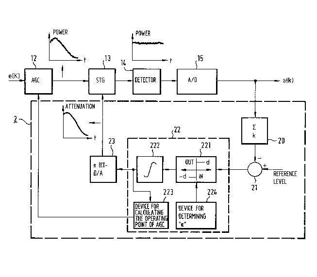
The sensitivity time control device 2, shown as a
block in Fig. 1 is shown in detail in Fig. 2. The
backscatter pulses e(k) received by means of the antenna 10
in Fig. 1 are amplified in the receiver device 11 and are
applied via the two attenuators switched in series in the
form of the automatic gain control attenuator (AGC) 12 and
the sensitivity time control attenuator (STC) 13 and via
the detector 14 to the A/D converter, where the backscatter
signal e(k) generated from the backscatter pulses is
digitized.
The digitized output values of the A/D converter
are averaged in a device 20 of the sensitivity time control
device 2, which generates an average value. In
- 4a -
.
202063q
this case the average value generation of the output curve
of the digitized backscatter signal e(k) is carried out
over several radar pulses, so that the average backscatter
signal power over the range can be estimated in this way.
The average backscatter signal power then is
compared in a comparator device 21 with a reference level
which corresponds to the desired nomin~l power. The output
signal of the--------------------------------------------
- 4b -
,~
2`~206~
comparator device 21 is subsequently controlled in the control
device 22; adaptive control takes place in an i~e~l on-off
relay 221 of the control device 22. A device 224 for
determining the control parameter d of the ;~ on-off
relay 221 is connected with it.
The following advantages are brought about with such an
~ l on-off relay control. The amplification factor of the
control path is not constant and can be greatly changed by the
received backscatter signal e(k). However, in this connection the
stability of the ~do~l on-off relay 221 does not
depend on the amplification factor.
Because an integrating member 222 is switched downstream
of the ido~l on-ff relay 221 it is possible to
perform discrete operations very easily and quickly. Any self-
oscillation of the control value occurring in this case does not
disturb the system as long as the amplitude remains sufficiently
small. The adaptation is also mainly used to shorten the response
time and to keep the self-oscillation as low as possible.
The adaptation used is performed similar to the process
of successive approximation. For this purpose an n-bit digital-
analog (D/A) converter 23 is switched downstream of the control
device 22 or the integrating member 222, by means of which the
digital signal at the output of the control device 22 is converted
into an analog voltage for the control of the sensitivity time
control attenuator (STC) 13, as indicated by the curve shown at the
upper left of block 23.
~20639
Calculation of the parameter "d", by means of which the
i~eal on-off relay 221 is controlled, is again
performed in accordance with already performed iteration steps.
The integrating member 222 is initialized with 2n/2, which
corresponds to half the range of the n-bit D/A converter. This
Means that in the first iteration step the parameter of the
dc~l on-off relay 221 is set to 1/4 of the n-bit
range,i.e. 2n/4. In the course of the following iteration steps
the valueof the parameter ~d~ continues to be halved until 1/2n of
the n-bit range, i.e. 1, has been reached. If at this time more
iteration steps are desired or required, the parameter of the
i~ ~ 1 on-off relay 221 always remains one (1). Therefore
control can be basically performed in n iteration steps(for
example: n = 8 for an 8-bit D/A converter).
Such a control is then performed in the sensitivity time
control attenuator 13 for all~ range gates, so that as a result a
sensitivity time control curve which depends on time is generated.
Because in practical application the signal is still noisy after
the average value generation in the device 20 because of the short
integration time filtering is
performed in the range direction before and after each
iteration step in the actually employed circuit devices,however,
this has not been separately shown in the block diagram of Fig. 2.
The output signal of the integrating member 222 is also
applied to a device 223 for calculating the operating point of the
automatic gain control attenuator 12. By means of optimal setting of
20~6~9
the operating point of the automatic gain control attenuator (AGC) 12,
corresponding optimization of the operating point of the
sensitivity time controlattenuator 13 is performed.
The algorithm for this can be described as follows: the
sensitivity time control attenuator is initialized, i.e. by means of the
initialization an amplification provided for the automatic gain
control attenuator (A~) 12. Subsequently a sensitivity time control
curve is generated, as already described above. Following each
such generation, the operational range of the attenuator in
the form of the sensitivity time controlattenuator (STC) 13 is
checked.
If the operational range of t~e STC-attenuator is
optimal, the sensitivity time control device reports to the user
that control was successful. But if the operational range of the
STC-attenuator is not optimal, a new amplification of the AGC
attenuator 12 is calculated and programmed by the device 223.
It is then necessary to generate
a new sensitivity time control curve, as already mentioned above.
After performing the algorithm, the operational range of the A/D
converter 15 as well as of the sensitivity ti.me controlattenuator (STC)
13 of the imaging radar system is optimized.
It is also possible to implement the sensitivity time
control device in connection with sonar or lidar.
The foregoing description of the specific embodiments
will so fully reveal the general nature of the invention that
20~ 3
others can, by applying current knowledge, readily modify and/or
adapt for various applications such specific embodiments without
departing from the generic concept, and, therefore, such adapta-
tions and modifications should and are intended to be comprehended
within the meaning and range of equivalents of the disclosed
embodiments. It is to be understood that the phraseology or
terminology employed herein is for the purpose of description and
not of limitation.