Note: Descriptions are shown in the official language in which they were submitted.
CA 02021095 2000-08-22
RD-18, 544
FIELD CONTROLLED DIODE (FCD) HAVING MOS TRENCH GATES
RELATED APPLICATIONS
This application is related to U.S Patent No. 4963950 issued October 16, 1990
to the present inventors and entitled, "Metal Oxide Semiconductor Gated Turn-
Off
Thyristor Having an Interleaved Structure".
BACKGROUND OF THE INVENTION
FIELD OF THE INVENTION
The present invention relates to field controlled diodes (FCD's), and more
particularly, to field controlled diodes having reduced gate current levels
during turn-
off.
BACKGROUND INFORMATION
The field controlled diode is a PIN junction diode in which current flow in
the
reverse direction is blocked by the junction of the diode and in which current
flow in
the forward direction may be blocked by application of an appropriate voltage
to a
junction gate to pinch off the cathode-to-anode current path of the diode.
When a
forward bias voltage is applied across the anode/cathode circuit of the field
controlled
15 diode and the field controlled diode is held in the off state by the bias
voltage applied
to the junction gate electrode, there is substantially no current flow between
the anode
and cathode electrodes. However, a current which can vary between small and
significant flows in the gate circuit because a reverse bias is applied to the
gate junction
to create the depletion region which pinches off the anodelcathode conductive
path.
2o This reverse biased junction collects any thermally generated carriers
which would
otherwise flow in the anode/cathode circuit. The level of this gate current
depends on
the diode's characteristics
n s~ -
sd ; ' 's
e.
.. 2 .~ ~ Oi ~J .t.. Y.,'~ Ci' C7
RD'18, 599
and the ambient~temperature and radiation conditions, since
thermally generated carriers and optically generated carriers
both add to the gate current. In order to allow the diode to
become conductive under these conditions, the applied gate
bias voltage is changed to one which reduces the reverse bias
on the gate junction to a level at which the anode/cathode
current path is no longer pinched off. Current is then
carried in the anode/cathode circuit in the normal manner for
junction diodes. Consequently, when the diode is ON, a
significant stored charge develops in the body of the diode.
When it is desired to turn the diode off by gate
control, a gate bias voltage is applied to the gate electrode
which reverse biases the gate junction and produces a
depletion region associated with that junction which
eventually pinches off the anode/cathode current path.
Unfortunately, in order for that depletion region to be
depleted of mobile carriers, a substantial portion of the
stored charge in the body of the diode must cross the
gate/diode junction to be collected by the gate region. This
produces substantial gate currents which may be on the order
of 50% of the ON-state current of the field controlled diode.
Once the gate junction depletion region pinches off the
anode/cathode path of the device and the stored charge has
been dissipated, the gate current drops to the quiescent
value in the manner discussed above. '
Unfortunately, the requirement for dissipating the
stored charge during the turn-off process for a field
controlled diode results in a relatively long switching time
for the field controlled diode and the dissipation of
substantial power during the turn-off process. Further, the
high gate current during turn-off, establishes the power
handling capacity which is required in the gate control
circuit and that circuit must therefore be capable of
handling substantial power.
n, G~ .a i~ . ...
t J "a
~J .x'.. 'r: v
- 3 -
RD-18,5~~
There is a need for a field controlled diode
providing low gate current turn-off of the diode.
Obiecs-a Of ha Tn~»nt a nr
Accordingly, a primary object of the present
invention is to provide a field controlled diode structure
employing an MOS gate rather than a junction gate.
Another object of the present invention is to
provide a field controlled diode having very low gate circuit
currents.
Another object of the present invention is to
provide a field controlled diode in which positive control of
the state of the diode is provided by a gate bias voltage
with minimal current flow.
Still another object of the present invention is to
provide a rapid turn-off field controlled diode.
Summary of h Tn~ent~~n
The above and other objects which will become
apparent from the specification as a whole, including the
drawings, are accomplished in accordance with a preferred
embodiment of the present invention through provision of a
field controlled diode having an MOS gate disposed in a
trench structure with the pedestals between the gate
electrode segments being narrow enough that application of an
appropriate gate bias voltage to the insulated gate electrode
pinches off the portion of the cathode/anode current disposed
within the pedestal. The turn-off time for this structure
may be shortened by including bipolar transistor segments
which do not pinch off interspersed with the diode segments
in order to provide a current path for extracting stored
charge from the body of the diode. These transistor segments
are preferably connected directly between the anode and
cathode electrodes so that the high current associated with
_ 4 - s ~i i:~ ~~ .'
RD-18,S44
extraction of the stored charge is part of the main current
path of the device and not part of the gate circuit whereby
the gate circuit carries no large currents.
Brief DEQP'ri r~+W On O h D a~.ri nnc
S The subject matter which is regarded as the
invention is particularly pointed out and distinctly claimed
in the concluding portion of the specification. The
invention, however, both as to organization and method of
practice, together with further objects and advantages
thereof, may best be understood by reference to the following
description taken in connection with the accompanying
drawings in which:
Figures 1 and 2 are perspective cross-section
illustrations of prior art junction gate field controlled
diodes;
Figure 3 is a perspective cross-section view of one
embodiment of a field controlled diode in accordance with the
present invention; and
Figures 4-16 illustrate alternate configurations
for the structure in accordance with the present invention.
netailed De4. ~Dt~on
In Figure 1, a prior art surface gate, field
controlled diode (FCD) 10 is illustrated.in perspective
cross-section view. In device 10, the P+ region 12 serves as
the anode region of the diode and the electrode 32 serves as
the anode electrode of the diode. The N type region 19
serves as the drift region of this PIN diode and the N+
region 16 serves as the cathode contact portion of the diode.
The metallization 36 serves as the cathode electrode of the
diode. P+ gate regions 24 are diffused into the upper
surface of the drift region 14 and have gale metallization 34
disposed in ohmic contact therewith. The lateral spacing S
- ~; ., , . .
li 4~r ~.'. '.." .~' '..?
RD-18,544
between the P+ gate regions 24 is selected in accordance with
the desired gate voltage for pinching off the drift region 14
between the anode region 12 and the cathode region 16. As
illustrated by the dashed line 22, the depletion regions
5 associated with the PN junction between the drift region 14
and the gate region 24 extend outward from adjacent the P+
regions 24 and merge under the cathode region 16 in a manner
which pinches off the drift region 14, thereby blocking the
current path from the P+ anode region 12 to the N+ cathode
region 16. The dotted portions of the lines 22 indicate
where the edge of one depletion region would be if the
adjacent P+ region were omitted, thus, the dotted portions
are within the pinched-off region. When a turn-off gate
voltage is applied between the gate and cathode regions, the
depletion regions 22 merge and prevent diode conduction
between the anode and cathode electrodes even in the presence
of a cathode-to-anode bias voltage of a polarity and
magnitude which would normally forward bias the diode,
turning it on. The device is rendered conductive under these
conditions by reducing the gate bias voltage to a level at
which the depletion regions no longer merge under the cathode
region 16 thereby allowing normal diode forward conduction to
begin. For maximum forward current in this field controlled
diode, the gate bias voltage is reduced to zero in order to
substantially eliminate the depletion region 22.
Once this diode is conducting in the forward
direction, it may be turned off by reversing the voltage
across the anode/cathode circuit in the well-known manner of
commutating a normal junction diode. In addition, this
device may be turned off by re-applying a gate bias voltage
of say 30 volts in order to extend the depletion regions 22
to intersect and pinch off the drift region 14 underneath the
cathode region 16.
_ 6 - ' ~ v ',..
~,~ SJ L:~ s_ iY' v.
RD-18, 544
During the ON-state of this diode, a substantial
stored charge develops in the drift region of this device as
is normal in PIN junction diodes. During turn-off of the
device, this stored charge must be dissipated as part of the
turn-off process. This charge dissipates by a combination of
recombination within the drift region (a relatively slow
process for a low ON-voltage diode) and by extraction of
holes through the gate region 24 and a simultaneous equal
extraction of electrons through the cathode region 16. As
these charge carriers are extracted through the gate region
24 and the cathode region 16, the depletion regions 22 spread -
until they merge under the cathode, thereby cutting off the
anode/cathode current path. The excess charge carriers
remaining in the non-pinched off portion of the drift region
14 dissipate by recombination and traversal of the depletion
region to the gate region 24. Once the stored charge is
dissipated, the diode is in the OFF-state with a minimal
reverse current which results from thermal generation of
carriers within the device structure. Some of this reverse
current flows in the cathode/anode circuit and some of it
flows in the cathode/gate circuit depending on the location
in which the carrier pair is thermally generated.
A modified (recessed gate) version of the junction
gate field controlled diode is illustrated generally at 10'
in Figure 2 in a perspective cross-section view. This device
structure is substantially similar to the structure of the
device 10 and the same reference numerals have been used for
corresponding structures in both devices. The primary
difference between these two structures is the fact that the
gate region 24 in the recessed gate structure 10' is formed
by first forming trenches in the cathode surface of the
device and then diffusing in the P+ gate region. From the
process point of view, this has the advantage that deep P+
regions da not have to be diffused into the drift region 14,
n~,;. . ;,.,~,
~~ ;. .'
- 7 - ~~~~;~_:_, .
RD-18,549
since the desired relationship between the gate regions 24
and the drift and cathode regions is achieved by the etching
of the trenches within which the gate regions are diffused
rather than by deep diffusion. This recessed gate device 10~
operates in substantially the same manner as the device 10.
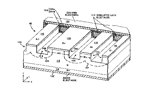
In Figure 3, a small portion of a field controlled
diode in accordance with the present invention is illustrated
generally at 110 in a perspective cross-section view. In
Figure 3, reference numerals in the 100's axe utilized. In
each of the figures, reference numerals ending in the same
two digits refer to corresponding structure in the different
devices and where the structure serves the same purpose
without significant modification in operation or function,
some of those portions of the structure may not be discussed
in connection with a given figure and the reader is referred
to an earlier discussion of that structure for its function
and purpose.
The device 110 comprises a plurality of Y-direction
extending pedestals separated by intervening gate trenches
144 in Which an insulated gate electrode 134 is disposed.
The insulated gate electrode 134 and the cathode
metallization 136 are illustrated only toward the back of the
figure in order to clearly illustrate the remainder of the
structure. The insulated gate electrode comprises a gate
dielectric (preferably thermal oxide for.silicon) layer 134a
and a conductor 139b such as polysilicon.
This device comprises a plurality of diode
pedestals 146 which are X-direction interspersed with a
plurality of transistor pedestals 148, although only one
transistor pedestal 148 is shown in the illustration. The
diode pedestals or segments 146 in which the cathode region
116 is disposed have a width WD which is small enough that
upon application of an appropriate gate bias voltage, say -15
volts, to the insulated gate electrodes 134, the portion of
- ~ ~ ~. _~_ :, ; r_;t
RD-19,544
the drift region within the pedestal is pinched off by the
depletion region which is induced in the N type drift region
by the applied gate voltage. The transistor pedestals or
segments 148 in which a P+ collector region 118 is disposed
have a width WT which is great enough that the depletion
regions 122 do not merge and deplete the drift region _
portions of those pedestals. In this way, the current path
from the anode region 112 through the drift region 114 to the
P+ collector region 118 is not pinched off. The P type anode
region 112, the N type drift region 114 and the P type
collector region 118 form a PNP transistor whose base current
is provided by the stored charge within the drift region.
This PNP transistor is connected directly between the anode
and cathode electrodes of the FCD so that the transistor's
collector current is part of the external cathode current of
the FCD rather than part of a gate circuit current. During
the process of turning off, the transistor helps dissipate
stored charge. This speeds device turn-off and when the
stored charge has dissipated, the transistor turns off
because of a lack of base current and the device is off.
Very little current flows in the insulated gate electrode or
its gate circuit during turn-off because of its insulated
nature. While the field controlled diode is in the ON-state,
some of the device current is carried in this PNP transistor
as a result of tha base current provided.by the stored charge
in the drift region. However, the majority of current is
carried in the diode structure, especially where a plurality
of diode pedestals are disposed between adjacent transistor
pedestals in the structure. The number of diode pedestals
146 disposed between adjacent transistor pedestals 148 is a
matter of design choice and is selected primarily in
accordance with the desired turn-off speed of the field
controlled diode which establishes the maximum allowable
diffusion time for stored charge to reach a transistor
g _ ~~ i~, s, .
r~ '~ E., ~. i' G;' ~4
RD-18,544 ,
pedestal. This'maximum diffusion time increases with
increases in the separation between adjacent transistor
pedestals and thus increases with increasing numbers of diode
pedestals disposed between adjacent transistor pedestals. In
this manner, during turn-off of the device, stored charge is
dissipated by Conduction through the pedestals 148 to the P+
collector region 118 in a manner which is similar to that in
which minority Charge is removed by the gate region 24 in the
prior art junction gate device. However, the circuit
consequences of that charge removal are substantially
different. As can be seen toward the back of Figure 3, the
cathode electrode 136 is disposed in ohmic contact both with
the N+ cathode regions 116 and the P+ collector region 118
whereby the current flowing into the P+ region 118 flows in
the anode/cathode circuit of the structure and not in the
gate circuit. In this manner, the gate current is kept to a '
minimum and is essentially that current necessary to charge
up the gate capacitance. This device, similar to the prior
art device, is turned on in the presence of a forward diode
voltage by reducing the insulated gate bias voltage to a
level at which the pedestals 146 are not pinched off. When
the diode is in the ON-state, the device is turned off by
applying an insulated gate bias voltage sufficient to deplete
the pedestal 146 portions of the drift region, or by
commutation of the externally applied anode/cathode voltage.
Not only does this structure drastically reduce the
gate current necessary to turn the device off, but it also
provides a relatively rapid turn-off for this device by
providing a current path through the P+ region 118 which
facilitates the extraction of stored minority charge from the
device structure.
In Figure 4, an alternative version of the Figure 3
structure is illustrated in which the gate. trenches 144' form
a grid configuration rather than the parallel stripe
~ ~,~ ~.! .(. ..: L' ii
RD-18,544
configuration of Figure 3. The device structure is otherwise
similar. In Figure 9, the gate electrode 134 and the cathode
electrode 136 are omitted from the drawing for drawing
clarity.
5 In Figure 5, another alternative version of a
device in accordance with the present invention is
illustrated generally at 210 in a perspective cross-section
view. The device 210 differs from the device 110 in that all
of the pedestal segments (both 246 and 248) have a uniform
10 width (WT = WD) in the X-direction and in the fact that the P
type collector region 218 extends the full height of the
pedestal portion 248 rather than being disposed only in the
top portion of the pedestal as shawn in Figure 3. As a
result of the entire pedestal height being occupied by the P
type collector region, the N type drift region 214 does not
extend into the pedestals 248 and the applied insulated gate
bias voltage does not pinch off the current path from the
anode 212 to the P type collector region 218 despite the fact
that the pedestals 248 are the same width as the pedestals
246.
The ratio of diode area to transistor area (region
216 area to region 218 area) which is optimum for a given
device depends on the intended use of the device and the
desired ON-resistance and turn-off time. Where a short turn-
off time is considered paramount, the diode and transistor
areas may preferably be substantially equal. As low ON-
resistance and small chip size become more important, the
ratio of diode area to transistor area should be increased to
minimize ON-resistance for a given chip area. Tncreasing the
cathode region area to collector region area ratio carries
with it an increase in device turn-off time (decrease in
speed) because of the increased maximum diffusion distance
far a stored charge carrier in the drift region to reach one
of the transistor connections to the power electrodes.
- 11 - :-~ ~t .~ .~ ., , r.
,, , ,
i1 i,~ _i~_ ~:v ,_t.5
RD-18,544
Devices in accordance with this invention may be
fabricated in a number of ways. It is considered preferable
to first define or form the N+ region 116 and the P+ region
118 and to then etch or otherwise form the trench structure
144. Where trenches are desired which are narrower than the
trench depth, with the result that diffusing the deep P+
region 218 of device 210 (Figure 5) prior to etching the
trenches would result in the P+ region 218 extending into the
pedestals 246 in which only a cathode region 216 is desired,
such diffusion is preferably prevented or avoided by
implanting the P type dopant material into the region in
which the pedestal 148 will be formed, but not driving that
diffusion until after trench formation. In this way lateral
X-direction spreading of the P type region is prevented by
the trench structure. In order to provide the shallow N+
regions 216, the pedestals 148 must then be masked and the N
type,dopant introduced into the pedestals 246 or else, a
relatively slow diffusing N type dopant and a relatively fast
diffusing P type dopant or different implant depths must be
employed in order to prevent pinch off of the pedestals 248
while ensuring pinch off of the pedestals 246 upon
application of an appropriate turn-off voltage to the
insulated gate electrode.
In Figure 6, an alternative version 210' of the
device 210 is illustrated. The structure of this device is
similar to that of device 210 except for the fact that rather
than having some pedestal segments in which no P type
collector region 218 is present and other pedestal segments
in which no N+ cathode region 216 is present, each
longitudinal (Y-direction) pedestal segment may contain both
an N+ region 216 and a P+ region 218 with the P+ region
extending the full depth of the pedestgl. This structure,
like the structure 210, prevents the pinch. off of the current
12 _ s~ ~t :, ~_ -e a:.~ < d
RD-18,594
path from the ainode 212 through the p type collector region
218 to the cathode electrode 236.
In Figure 7, a further alternative embodiment 210"
of the device 210 is illustrated. This device is like the
device of 210 excegt for the trench structure 244" being in
the form of a grid structure rather than in the form of
parallel stripes as was the case in device 210.
In Figure 8, a further alternative structure for
the device 210 is illustrated at 210*. The configuration of
the pedestals in the device 210* is similar to that in the
device 210, with the exception that none of the pedestals
contain a P type region and each of the pedestals is pinched
off at the same applied insulated gate bias voltage. This
device structure has a disadvantage as compared to the device
structure 210 in that it takes longer to turn off because of
the absence of a P+ region suitable for extracting stored
charge from the structure during turn-off. As a consequence,
the stored charge is dissipated primarily by recombination
with the result that the turn-off time for the device
structure is increased and~the safe operating area for the
device is decreased because of the substantial quantity of
stored charge present in the structure during turn-off.
In Figure 9, a further alternative device structure
310 is illustrated. The device structure 310 is an
alternative version of the structure 210' in that each of the
Y-direction extending pedestals which is illustrated in the
figure, contains both an N+ cathode region 316 and a p+
collector region 318. This structure differs from that of
the device 210' in Figure 6 because the P+ region 318 does
not extend to the bottom of the pedestal and because the
pedestal is wider at the P+ collector region 318 than at the
N+ region 316 in order to prevent pinch off of the pedestal
portion of the N type drift region 319 under the P+ collector
region 318.
- 13 - ~ ~~ :~ _,. °..' ::> e9
RD-18,544
The device 310' illustrated in Figure 10 is like
the device 310, except that the P+ collector regions 318 in
adjacent pedestals are displaced from each other in the Y-
direction, thereby reducing the minimum permissible X-
direction center-to-center spacing of the pedestals in order
to allow adequate space for the gate electrodes.
A further alternative structure 310" is shown in '
Figure 11 in which the P+ collector region 318 is made
continuous in the X-direction between adjacent "pedestals" by
not etching the trench through the P+ collector region.
While in each of the figures a trench structure
extending into the semiconductor body from the cathode side
of the structure is illustrated, the conductivity type of all
regions can be reversed to provide the complementary field
controlled diode. Such a reversal is not preferred in
silicon because of the substantially higher mobility of
electrons than holes in silicon.
While the trench structures illustrated are either
Y-direction extending parallel segments or a grid
configuration, the trench structure may alternatively have a
concentric, circular, rectangular or other configuration, if
desired. The significant feature of the invention being the
provision of a field controlled diode having an insulated
gate for conductivity control and preferably the provision of
a transistor structure in the field controlled diode to
facilita,,te more rapid turn-off of the device upon application
of a turn-off insulated gate bias voltage to the insulated
gate.
Each of the above discussed and illustrated
structures is a vertical device in which the main current
flow is vertical through the semiconductor chip perpendicular
to the major surfaces of the wafer in which the chip was
fabricated. Field controlled diodes in accordance with the
present invention may also be fabricated as lateral devices.
.,
Y4P ~(,1 5".' ..i.. <. a.l i.~
- 14 -
RD-18,549
Such lateral structures are illustrated. in perspective cross-
section views in Figures 12-15. In Figure 12, the device 910
is a multicellular device in which the structure at the
lefthand side of the figure alternates in the X-direction
with the structure at the righthand side of the figure
whereby current from the anode region 412 flows both to the
left and right in the figure. In this device structure, the
gate electrodes are disposed in the trenches 444 which divide
the cathode region 416 into a plurality of Y-direction spaced
apart segments. The width WD of the "pedestal" between two
Y-direction adjacent trench segments 494 is made narrow.
enough that application of an appropriate gate bias voltage
to the insulated gate disposed in the trenches pinches off
that pedestal, thereby interrupting current flow to the
cathode region 416. In device 410, the ON-state current
flows laterally and primarily near the upper surface of the
semiconductor body. During turn-off, current flow is blocked
through the pedestal portions of the structure with the
result that the current during turn-off, which is indicated
by the dashed line in Figure 12, must flow deeper into the
semiconductor body than the bottom of the trenches in
reaching the P+ region 418.
The device 410' in Figure 13 is similar to the
device 410, except for the absence of a p+ region 418. I
Device 510 in Figure 14 is similar to devices 410
in being a lateral device. It differs in that the trenches
594 extend in the Y-direction and space the cathode region
516 from the anode region 512. Consequently, in this device
structure, the ON-state current must flow beneath the gate
electrodes to reach either the cathode region 516 or the
collector region 518. This structure is also a multicellular
structure in which the structure at the righthand side of the
figure alternates in the X-direction with the structure at
the lefthand side of the figure.
y n c., .
s, ,
- 15 - .'.I ks e~ ~ . ..
RD-18,544
The device 510' illustrated in Figure 15 is similar
to the device 510 except for the absence of a P+ region 518
from the structure of the device 510'. Again, it is a
multicellular structure.
In each of Figures 12-15, the device is illustrated
as being formed on a P+ substrate, however, it may
alternatively be formed in a dielectric or junction isolated
region and may be a discrete device or part of an integrated
circuit.
In Figure 16, a higher speed version 110" of the
device 110 of Figure 3 is illustrated. In device 110", the
anode region 112" is grid shaped with openings therein in
which the drift region 114" extends into contact with the
anade electrode 132, or the region 114" contact with the
anode electrode is grid shaped with the anode region 112"
comprising separate segments disposed in the openings in that
grid or combinations and variations on such structures. The
anode electrode material is selected to provide a Schottky
barrier where it contacts the N type drift region 114". In
this way, hole injection into the drift region 114" during
the ON-state is reduced, since part of the current is carried
through the Schottky diode thereby reducing the stored charge
and speeding device turn-off. Schottky barriers of this type
may be included in the device structures shown in the other
figures as ~aell.
This device may be a normally on device as has been
described, or may be a normally off device. Where the doping
leval of the N type region 114 is low enough (about 1 x 10¹³
dopant atoms per cm3) and the mesa width WD is narrow enough
that the gate electrode work function is large enough that
the entire mesa width is pinched off at the zero gate bias,
the device is normally off.
A wide variety of device structures and pedestal
configurations have been illustrated. Features of different
M ~r 4 ~~~. ~L c. r r
RD-18,544
device structures may be combined in a single different
structure in any desired manner. All such combinations and
permutations axe considered to be within the scope of the
present invention as defined in the appended claims.
While the invention has been described in detail
herein in accord with certain preferred embodiments thereof,
many modifications and changes therein may be effected by
those skilled in the art. Accordingly, it is intended by the
appended claims to cover all such modifications and changes
as fall within the true spirit and scope of the invention.