Note: Descriptions are shown in the official language in which they were submitted.
~02~;~9~ :
25307-245 : ~
', ' ' .~:
BACKGROUND OF THE IN~7ENTION . ~
. ,:
The present in~ention relates to a polarity detector .
for subscriber lines for detecting a polarity of subscriber lines
in a data transmitting system having 2-wire subscriber lines using
2BlQ (two binary - one quaternary) codes.
BRIEF DESCRIPTION OF THE DRAWINGS
Figure 1 is a block diagram of a digital subscriber -
line system;
Figure 2 is a diagram of a super frame on the subscriber
line in Figure l; `
Figure 3 is a detailed block diagram of a 2-wire sub~
scriber line and subscriber line and subscriber line terminator
in Figure l;
Figure 4 is a timing diagram for the 2BlQ code; .. ;
Figure 5 is a block diagram of the present invention;
Figure 6 is a block diagram of a first embodiment ;
according to the present invention;
Figure 7 is a timing diagram of a training pattern; :~
Figure 8 is a diagram of a signal pattern;
Figure 9 is a block diagram of a second embodiment
accordlng to the present invention; ~:
Figure 10 is a block diagram of the synchronizing
signal detector in Figure 9;
~ .,,,:
Figure 11 is a block diagram of a polarity detector in ~ .
Figure 9; .. : .
Figures 12 and 13 are diagrams explaining operations
- 1 - - .; ;'i .'
--" 2021;~
25307-245
of the second embodiment according to the present invention; -
Figures 14 and 15 are block diagrams of a third embodi~
ment according to the present invention; and
Figure 16 is a timing diagram for explaining the -
operation of the third embodiment of the present invention shown
in Figures 14 and 15.
In the 2BlQ code, "1", "1" in binary notation is set to
+1 in quaternary notation, "1", "0" in binary notation is set to +3
in quaternary notation, "0", "1" in binary notation is set to -1 in ~`~
quaternary notation and "0", "0" in binary notation is set to -3 in ;;-~
quaternary notation. Development of a point U interface for an
Integrated Services Digital Network (ISDN) using a 2BlQ code as ;~
described above has been ongoing. If the connecting polarity f !~
the 2-wire subscriber lines of the point U interface is inverted,
when quaternary code is converted to binary code through polarity
inversion, the binary code on the receiving side is different from
that on the sending side. The~efore, it is essential to correctly ~ t,
decode the quaternary code by deciding whether or not the connect-
ing polarity of the 2-wire subscriber lines has been inverted. ~c!-
Development of a 2-wire subscriber line transmission
system using the 2BlQ code for an ISDN has been continuing. For `~
instance, in Figure 1, a subscriber terminal 101 is connected to ~;
. ~
an office line control unit OCU 103 by a 2-wire subscriber line ~;
104 through a distributed subscriber line
, ~
- la -
202129~ ~ ~
control unit DSU 102. The 2BlQ code data is transmitted to
the subscriber line 104. ~he distributed subscriber line
control unit 102 and the office line control unit 103, -~
respectively, include interfaces 105 and llo, line
............................................................................. ................................. ~.... .
controllers 106 and 109, and subscriber line terminators 107
and 108. The line controllers 106 and 109 are provided with
functions for multiplexing and demultiplexing control of the
subscriber terminators 107 and 108, and functions for code
~ ~ .
conversion from binary to quaternary code and timing --
extraction.
Fig. 2 is a chart of sending frames in binary code. A ~ -
super frame is formed by eight frames from #l to #8. The
period of each frame is 1.5 ms and is formed by an 18 bits
inversion frame synchronous signal ISW or a frame
synchronous signal SW, 216 bits of (2B+D) x 12 data and a 6
bits M channel. The letter B in 2B+D indicates a B channel
of 64 Kbps, while the letter D indicates a D channel of 16
Kbps.
The 2-wire subscriber line transmission system using
the 2BlQ code explained above is standardized by the ~
American National Standards Institute Regulation which -
6pecifies that a couple of lines are sometimes connected
through two inversion lines. It is required that normal
data transmission be realized even when the connecting
polarity of the 2-wire subscriber lines 104 is inverted.
2 ~
~: - : : , .
202~295 : ~
The subscriber line terminators 107 and 108 of the
digital subscriber system shown in Fig. 1 are shown in more
detail in Fig. 3. The office line control unit (ocu) 103 is
connected to a TIP terminal and a RING terminal of the ~ -
subscriber line 104 through a hybrid transformer 1081. The
line controller 109 assembles the data sent from an exchange ;
to the sending frame having the format shown in Fig. 2 and
then sends the frame to the code converter 1083. The code
converter 1083 converts a binary non-return-to-zero (NRZ)
code sent from the line controller 109 into a quaternary ;~
2BlQ code, amplifies it up to a predetermined level and
thereafter, sends it to a balance/unbalance converter 1082.
The balance/unbalance converter 1082 performs a
balance/unbalance conversion of the 2BlQ code sent from the ,
code converter 1083 in order to send it through the hybrid
transformer 1081 and over the 2-wire subscriber line 104.
Thus, the data sent from the exchange is transmitted to the
distributed subscriber line control unit 102 through the 2-
I wire subscriber line 104.
¦ 20 The 2BlQ data from the distributed subscriber line
control unit 102 i8 sent through the 2-wire subscriber unit
104 and the hybrid transformer 1081 and is received by a
balance/unbalance conversion circuit 1085. The
balance/unbalance conversion circuit 1085 differentially ;
amplifies the signal waveform appearing across the TIP
terminal and the RING terminal. The differentially
. ,~ " . -.
.'~:, -:
2021~5 ~-
amplified signal on the 2-wire 6ubscriber line is waveform
equalized by an equalizing amplifier 1086 and a timing
signal is extracted therefrom. The code converter 1087
converts the 2BlQ code data sent from the equalizing
amplifier 1086 into binary NRZ data based on the extracted
timing signal and sends it to the line controller 1os. The ~ -~
line controller 109 demodulates the binary NRZ data sent
from the code converter 1087 (in the sending frame format `~
shown in Fig. 2) and sends it to an exchange through an ~ ~-
interface llo. Each section of the distributed subscriber
line control unit 102 operates in the same way as the office
line control unit 103. When the TIP and RING terminals of
the 2-wire subscriber line 104 are inversely connected, the
balance/unbalance converter 1085 outputs inverted 2BlQ code
data since it differentially amplifies the signal.
Figure 4 is a timing diagram for the operation of the
circuit shown in Figure 3. The waveform A in Fig. 4, which
is the 2BlQ code under normal polarity, is changed to the
waveform B by inverting the connecting polarity of the TIP
and RING terminals of the subscriber line 104. Therefore,
the binary code obtained by receiving and decoding the
waveform A is guite different from the binary code obtained
by receiving and decoding the waveform B. Accordingly, it
is necessary to receive correct data. This is accomplished
by detecting the connecting polarity of the subscriber line. ;~
,', ~ ' ~.',;
' ~ ''' ~ '''''
~. '''''.''','' .`'''''''.'
202129~
25307-245
SUHMARY OF THE INVENTION ;~
It is an object of the present invention to detect the
polarity of subscriber lines using a simplified structure. - `
According to one aspect, the present invention provides
a polarity detector for subscriber lines in a system for
transmitting a quaternary 2BlQ code over the subscriber line,s `-
said polarity detector comprising~
code converter means for converting the quaternary 2BlQ code ,
received through the subscriber lines into binary codes for
outputting complementary blnary data; ` .
frame synchronizing signal detector means for detecting and
outputting a frame synchronizing signal in the complementary
binary data output from said code converter means and outputting a . .~-
timing slgnal;
pattern detector means for detecting all "l"s or "O"s of the ~; .
complementary blnary data output from said code converter and a ;`
tlmlng slgnal from said frame synchronlzing signal detector means; .
and ;~
selector means for selecting all complementary binary data
havlng a single polarity from the complementary data pattern
output from said code converter means in response to a detection ~ ' ~"',r~
of all "l"s or "0"s by said pattern detector. ` ,:i:
According to another aspect, the present invention i-
provides a polarity detector for subscriber lines in a system for
transmitting a quaternary 2BlQ code over the subscriber llnes, , ~ :,
sald polarlty detector comprising, :~
code converter means for receiving the quaternary 2BlQ code
~
v~
-- 2 0 2 ~ 2 9 ~
25307-245 ~
`
over the subscriber lines and for converting the qua~ernary 2BlQ
code into binary code and outputting complementary binary data;
frame synchronizing signal detector means for receiving the
complementary binary data, detecting a frame synchronizing signal
in the complemçntary binary data and outputting a frame
synchronizing signal;
pattern detector means for detecting an all "l"s or "O"s -~
state of the complementary binary data and the frame
synchronizatlon signal; and -:
selector means for selecting all complementary binary data .~
having a single polarity in response to the detection of an all ~ .
"l"s or "0"s state. - ~
DESCRIPTION OF THE PREFERRED EMBODIHENTS ~.
A polarity detector for subscriber lines according to ~:
the present invention detects the polarity of the subscriber lines
using a training pattern. The polarity detector of the present
inventlon wlll be explained with reference to Flgure 5. A code
converter 1 dlrectly converts a quaternary . ~-
. . .
. .
... .. . . .
. ,., .,, :,.. . ~ .:.
'"'''','',','''" ~
,: .,
:: .: . .:
,. .... - .. .
: :: .: ~: ,~. "
. , .... ~..
:.,'::: ;....
5a . ............... .
f~ ,.;,,.. "" ",.," ,,
20~
25307-245
2BlQ code received from the subscriber lines into a binary code
to obtain a positive binary data RDT. The code converter 1 also
inverts the received 2BlQ code and then converts the inverted 2BlQ
code into a binary code to obtain a negative binary code RD~
That is, the code converter 1 outputs complementary binary data '~
RD+ and RD-. For example, when code converter 1 receives A
pattern of 2BlQ code in Figure 4 from subscriber lines, it con- ~s~
verts A pattern into a positive binary data (~D+). At the same
time, it inverts A pattern and produces B pattern, and then it i~ -;
converts B pattern into a negative binary data (RD-). A synchroniz- ~;
ing signal detector 2 detects the frame synchronizing signal of
the binary code data of either positive binary data RD+ or negative ~.
binary data RD- sent from the code converter 1. Pattern detectors
3 and 4 detect whether the complementary data RD+ and RD- sent
from the coder converter 1 are set to predetermined all "l"s or
"O"s in synchronization with detection of frame synchronizing ~ ;- 1`
signals from the synchronizing signal detector 2. A selector 5 ' ;
6elects the data having a single polarity of the complementary
data RD+ and RD- sent from the code converter 1 along with detected
outputs from the pattern detectors 3 and 4.
It is also possible to form a device in which the ;~
selector 5 is controlled by detecting whether or not the inverted .....
frame synchronizing ^ignal and the frame synchronizing signal of .
the training pattern from the synchronizing signal detector 2 are
in a predetermined sequence. Moreover, the synchronizing signal ' '.!'' '
detector 2 may also be integrated in common with a frame synchro- :
nizinq protection aircuit.
-` 20Zl;~!~5
25307-245
The code converter 1 converts quaternary code and
inverted quaternary code into positive and negative binary codes
and outputs complementary data RD+ and RD-. The frame synchro~
nlzing signal is detected in the synchronizing signal detector
2 using RD+, for example, and the 216 bits data and the 6 bits ~ ~ -
M channel data of the training pattern shown in Figure 2 become
all "l"s or "O"s. Therefore, the pattern detectors 3 and 4
detect all the "l"s or "O"s. When all "l"s are detected in the
pattern detector 4, that is, when the data of the training pattern
is set to all "l"s, the inverted polarity of the subscriber line
is detected since the data RD- is correct data. Therefore, the ~;
selector 5 selectively outputs the data RD- as the received data
RD r
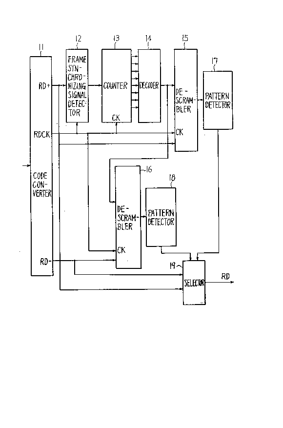
Figure 6 is a block diagram of a first embodiment
according to the present invention. Reference numeral 11 design- ~
ates a code converter which converts quaternary code into binary `
code and outputs complementary data RD+ and RD-, and a clock signal ~
RDCK. ~ ~;
The clock extracted from the received data is used for
convertlng received quaternary code into binary code (NRZ data)
in a code converter 11. i
A frame synchronization circuit, generally including `
a frame synchronizing signal detector, a frame synchronization
protectlon circuit and a hunting circuit for searching a real
frame synchronizing signal, is in code converter 11 to synchronize
RQCK with a olock ertrscted from received 2BlQ code. RDCK is a
ZOZ~2~
25307-245
clock in synchronism with RD+ and RD-. Reference numeral 12
designates a frame synchronizing signal detector which-detects
the frame synchronizing signal from the binary code data. Refer-
ence numeral 13 designates a 240-step counter which counts the
clock signals RDCK. Reference numeral 14 designates a decoder
which outputs an enable signal for descrambling 2B+D bits and M
bits. Reference numerals 15 and 16 designate descramblers which
descramble the complementary data RD+ and RD-. Reference ~`~-
numerals 17 and 18 designate pattern
"~
"` :~,,
'~
. ..
: . .. , ' . . .
,j ` ~ ~,
" ,', .~', ..
2021;~!~5
detectors which detect all "l"s or "o"s of the complementary
data RD+ and RD-. Reference numeral 19 designates a
selector.
The pattern detectors 3 and 4 in Fig. 5 correspond to a
structure formed by the descramblers 15 and 16 and the
pattern detectors 17 and 18. The frame synchronizing signal
detector 12 may be constructed to detect the frame
synchronizing signal included in the data having any single
polarity of the complementary data RD+ and RD-. The
descramblers 15 and 16 descramble the data, except for the
frame synchronizing signal, in the sending side.
The counter 13 is formed as a 240-step structure
because one frame is formed with 240 bits. The counter 13
counts the clock signal RDCK when "0" is loaded by the
detected signal of the frame synchronizing signal. The
counted value is applied to a decoder 14. The decoder 14 -~
applies the enable signal to the descramblers 15 and 16
during a period 222 bits after an initial 18 bits of one
: :., , :,.....
frame is excluded. Accordingly, the descrambling is carried~
out in the descramblers 15 and 16, excluding the frame
~ynchronizing signal.
The polarity of the bits is determined by detecting all
'll"s or "0"8 in the descrambled 2B+D bits and M bits in the
pattern detectors 17 and 18. The pattern detectors 17 and
18 may be realized with simple logic circuits. The selector
19 i5 controlled depending on the detection result. Any one
,,, i ., -
-, . ;,, ~,
':'".' ~'.'.'".,'.'.'
: .: . ,:
' `'~
2021~!~5
of the data RD+ and RD- is output as the receiving data RD
and the detection result is maintained until the end of
communication. ;
The structure of each circuit may be realized by logic
circuits and microprocessors, etc. The code converters 1074
and 1087 (refer to Figs. 1 and 3), in the subscriber line
terminators 107 and 108 in the digital subscriber line
system, determine the polarity of the data.
I Fig. 7 is a diagram explaining the training pattern.
j 10 Signals TN and SNl are transmitted to the office line ~ -
control unit 103 from the distributed subscriber line ;~
control unit 102 to set up a no-signal state. Thereafter,
! signals SN2 and SN3 are also transmitted. A signal TL is
transmitted to the distributed subscriber line control unit ~ `~
102 from the office line control unit 103 to set up a no-
¦ signal state. Then, signals SLl, SL2 and SL3 are also -
transmitted. During a no-signal period after the signals
have been transmitted, an echo canceller (not shown) is
I connected.
: .
The signals SN1 and SLl are transmitted when -
¢ommunication is started under an initial condition, that :
is, at a so-called cold start time. When communication is
completed, an equalizing circuit or echo canceller (neither ~;
are shown) maintains a converged state. A signal is not
25 transmitted when communication is started under a so-called
.: ., ~: . .;
warm start time.
'~' ~"' '.
,
' . ' " '"
~''
... ,....... ... ,...... ,,.. ,.. ~, ., .. ,.. ~.. " .. ,. ,., ,.. ,.. ~.... . . . . . ..... .. . . ....... .. .
,
Z02~2!~5
Fig. 8 is a diagram for explaining a signal pattern.
The signals TN and TL form a repeated pattern of +3 and -3
in quaternary notation or "1000" in binary notation. On the
other hand, the signals SNl, SN2 and SLl have a frame
structure including a frame synchronizing signal SW of +3, -~
+3, -3, -3, +3, -3, +3, +3 in quaternary notation and 211
"l"s in 2B+D bits and M bits. Signals SN3 and SL3 have a
frame structure including the frame synchronizing signal Sw,
any one of the inverted frame synchronizing signals ISW (-3, ~ -~
-3, +3, +3, +3, -3, +3, -3, -3), the 2i3+D bits and the M
bits used as ordinary data. The signal SL2 has a frame
structure including any one of the frame synchronizing ~ ~;
signal SW, the inverted frame signal ISW, 2B+D bits having
all "0"s and M bits having all "l"s.
The polarity detecting operation is started by
inputting the signals SNl, SN2, and SN3 or SN2 and SN3 as -- i
the training pattern to the office line control unit 103, -- .
and inputting the signals SLl, SL2, and SL3 or SL2, and SL3 :
to the distributed subscriber line control unit 102. A
frame synchronizing signal SW or an inverted frame ;-
~ynchronizing signal ISW is then detected using the frame ~ ,
~yn¢hronizing signal detector 12. The counter 13 starts ~.
counting the clock signal RDCK when the detected signal is
received. The decoder 14 adds the enable signal having 2B~D ; ;
bit~ and M bits to the descramblers 15 and 16. The
descrambled data is added to the pattern detectors 17 and
'"' ~',''"''''
.......... ~.... ".,,.,,,.,.,,.,,,., ~: '
,"'~.
. ~, . . . . . .. , , . . - . . . . ~ - -
zo~ "
18, and the signals SNl, SN2, and SLl having all "l"s are ,5''.:
detected.
For example, when the signals SNl, SN2, and SLl are
received, if an all "l"s state (+l in quaternary notation) -
is detected in the pattern detector 17, the data in which
"O"s and "l"s appear alternately (-1 in quaternary notation)
is input to the pattern detector 18. The selector 19 is
controlled by the detection signal from the pattern detector ~1`
17 and RD- is output as the receiving data RD. When the
signal SL2 is received, an all "O"s state is detected only
for the 2B+D bits. Although an all "O"s state means
quaternary -3, when quaternary -3 is attained through
polarity inversion, "l"s and "o"s alternately appear in the
binary code and therefore the all "O"s state is not
detected. `- ~-
Accordingly, it becomes possible to automatically ~-
detect the connection polarity of the subscriber lines ~ `:',;'.~'2
through transmission and reception of a training pattern 80 : ~.i
that correct data may be received.
Flg. 9 is a block diagram of a second embodiment ~ --
according to the present invention. In Fig. 9, reference
numeral 21 designate6 a code converter, reference numeral 22 --
designates synchronizing signal detector, reference numeral - ~ ;
23 designates a polarity detector, and reference numeral 24
designates a selector. In the second embodiment, a frame
synchronizing signal SW or an inverted frame synchronizing
12
~` 2021;~35
signal ISW is detected in the frame synchronizing signal
detector 22. The data having either of the polarities of
the complementary data RD+ and RD- are output from the code
converter 21. The detected frame synchronizing signal SWD ~-
or the detected inverted frame synchronizing signal ISWD is ~
added to the polarity detector 23. Polarity is detected in ~- -
accordance with the detection of either the SWD or ISWD
signal in a predetermined sequence. The polarity detection
~:. : . i
signal POL controls the selector 24. Any of the
¦ 10 complementary data RD~ and RD- is selected as the receiving
data RD and it is then transmitted to the data processor - -
(not illustrated).
The frame synchronizing signal detector 22 may have the ~
same structure as the synchronizing signal detector 12 shown --`in the embodiment of Fig. 6. Por example, the detector 22 -
can be formed as shown in Fig. lO. The detector 22 `
I sequentially shifts the data RD+ to a serial/parallel ~ `
I converter 31 in accordance with the clock RDCK to output 18
I bits in parallel and then adds such data to the gate
¦ 20 circuits 32 and 33. The gate circuit 32 detects the frame ~i
,. . . i
synchronizing signal SW shown in Fig. 4. The gate circuit ~
33 detects the inverted frame synchronizing signal ISW shown ~ ;
in Fig. 8.
The polarity detector 23 can be formed as shown, for
example, in Fig. 11. The polarity detector 23 includes
flip-flops 41 through 45, an 8 bits counter 47, AND circuits
13
...... ,.~., ''' ~"''.'
. . .:
, ~ `.; ''''~
%0212. ~35
48 through 53, an OR circuit 54 and inverters 55 and 56.
The detected signal SWD of the frame synchronizing signal SW
is applied to a load terminal LD of the counter 47 through a
terminal J in the flip-flop circuit 41 and the OR circuit -
54. The detected signal ISWD from the inverted frame
synchronizing signal ISW is applied to a terminal J in the
flip-fl~p 43 and a load terminal of the counter 47 through -
the OR circuit 54. Moreover, a reset signal RST is applied ~ ;`
to the reset terminal R of the flip-flops 41 through 44 and
the counter 47 during an initial condition and the clock
signal RDCK i5 applied to the clock terminal CK.
Therefore, during cold start, for example, the frame
synchronizing signal SW of the signals SNl and SLl is
detected. The detected signal SWD of the frame ~ -~
synchronizing signal SW can be continuously obtained two or
more times since the inverted frame synchronizing signal ISW `; -
is not included. If a second detected signal SWD is
obtained 240 bits after the first detected signal SWD, an
output signal of the AND circuit 52 becomes "1", the flip-
~lop 43 is set and the polarity detecting signal POL at the
Q output terminal of the flip-flop 45 becomes Nl~. When the
polarity detecting 6ignal POL has the level "1", the
selector 24 select~ the data RD~ as the receiving signal RD.
Since the connecting polarity of the subscriber line is
inverted, the frame synchronizing signal SW is also
inverted. The detected signal ISWD of the inverted frame
14
. . ............. . . . . . . .............. . . . .
, :
-`` 2021;~
synchronizing signal ISW is continuously obtained two or
more times. In addition, when the second detected signal
SWD is obtained 240 bits after the first detected signal
SWD, an output signal from the AND gate 53 becomes "1", the
flip-flop 45 is reset and the polarity detection signal POL
becomes "0". Since the polarity detection signal POL
becomes "0", the selector 24 selects the data RD- as the -~-
receiving signal RD. ;
If the signal SL2 is received under the warm start
condition, the frame synchronizing signal sW is received and --~
the inverted frame synchronizing signal ISW is also received
as a super frame synchronizing signal. When the connecting
polarity of the subscriber lines is inverted, after the - ;~
detected signal SWD of the frame synchronizing signal Sw is
obtained, the detected signal ISWD from the inverted frame - `
synchronizing signal ISW is continuously obtained seven or --~
more times. If the flip-flop 41 is set first, the flip- ~ `~
flops 43 and 44 are then set. Therefore, the flip-flop 45 ;
is reset by the output signal "1" from the AND circuit 53 ~:
and the polarity detection signal POL becomes HO~.'. ;
Figs. 12 and 13 are diagrams for explaining the~`
operation of the second embodiment explained above. In Fig.
12, the connecting polarity of the subscriber lines is
nor~al. That is, the training pattern has a frame structure
including a frame synchronizing signal SW, 2B+D bits and M
bits when RD+ data is received. When the detected signal
-. 2021~3~ ~
SWD of the frame synchronizing signal SW is continuously
obtained for two or more times, the Q terminals 41Q and 42Q
of the flip-flop 41 and 42, respectively, output a "1" and ; ~--
the polarity detecting signal POL becomes "1".
In Fig. 13, the connecting polarity of the subscriber ~-
lines is inverted. The frame synchronizing signal SW is -
received as the inverted frame synchronizing signal I5W and
2B+D bits and N bits are also inverted. When the detected
signal ISWD of the inverted frame synchronizing signal ISW
is continuously obtained two or more times, it becomes the
output at the Q terminals 43Q and 44Q of the flip-flops 43
and 44, respectively. Since the polarity detecting signal
POL becomes "0", the data RD- is selected.
Accordingly, the polarity of the subscriber lines can
be decided by detecting the frame synchronizing signal SW
and the inverted frame synchronizing signal ISW in the
training pattern. Figs. 14 and 15 are detailed block
diagrams of a third embodiment according to the present
invention. Reference numerals 61 through 63 designate flip-
flops, reference numerals 64 through 72 designate gate
circuits, and reference numeral 73 designates a
differentiation circuit (d/dt). Reference numerals 81
through 91 designate flip-flops, reference numerals 92
through 99 designate gate circuits, reference numeral 75
designates a 240-step basic frame counter, and reference
numeral 76 designates an octonary super frame counter. ;
" ::
16
.. . .. .... ........ .. .. .. ...
:
..
2021~9~ ~
The third embodiment shown in Fig. 14 is a structure in
which the polarity detector 23 and a part of a frame
synchronizing protection circuit are used in common. The
detected signal SWD of the frame synchronizing signal SW ;
sent from the synchronizing signal detector 22 (refer to
Figs. 9 and 10), the detected signal ISWD of the inverted
:: :.: .: --.
frame synchronizing signal ISW and a clock signal RDCK are
applied. A polarity is detected by flip-flops 82, 83, 8g, - -
90 and 61, as shown in Fig. 15. The flip-flops 82, 83, 89,
and 90 correspond to the flip-flops 41 and 44 shown in Fig.
11, while the flip-flop 61 corresponds to the flip-flop 45 -
shown in Fig. 11. --
The flip-flop 62 outputs a synchronization establishing ~-
signal BSYN of the basic frame. The flip-flop 63 outputs a
., .,: .:
synchronization establishing signal SSYN of the super frame.
The set signal of the flip-flop 63 is differentiated by a
differentiation circuit 73. The output signal RFCINT from
the differentiation circuit 73 is loaded into a counter 76
~see Fig. 15). The output signals F4 through F7, F11
through F13, and F21 through F23 from flip-flops 82 through ; ~;~
91 (Fig. 15) are applied to the gate circuits 64, 66, 67, ~ ~
and 69 through 72 (Fig. 14). ~ ;
Fig. 16 is a timing diagram for explaining the ~ ;
operations of the circuits shown in Figs. 14 and 15. The
waveforms are identified by the signals shown in Figs. 14
and 15. When the detected signal SWD of the frame :
17 ~
: ~ ~;',".';
' ~ ' . ;' ~'
. `' . .
20Z~ 5
synchronizing signal sw and the detected signal ISWD of the ~
inverted frame synchronizing signal ISW are input as~ ~ -
indicated in Figs. 14 and 15, an output signal al from the : 1-~
~ gate circuit 95 changes as shown in Fig. 16 and is input to
¦ 5 the counter 75. An output signal a2 from the gate circuit
97 becomes "o" because the flip-flop 81 is set by the first
detected signal SWD. The flip-flop 82 is also set and its ` -- -
output signal Fll becomes "1". :-
When the second detected signal SWD is applied, the .
flip-flop 83 is set and its output signal becomes "1".
Therefore, the output signals Fll and F12 are "1". An
output signal from the gate circuit 69 also becomes "1", and
sets the flip-flop 61 which outputs the polarity detecting
signal POL which becomes "1". Thus, the polarity of the
~ 15 subscriber lines is normal and the data RD+ is selectively
¦ output by the selector (not illustrated). Moreover, since
the flip-flop 62 is also set, the synchronization .:~
establishing signal BSYN of the basic frame becomes "1".
' When a third detected signal SWD is applied, the flip-
flop 84 is set and its output signal F13 becomes ~1". When
the detected signal ISWD of the next frame synchronizing
~ignal ISW is applied, the flip-flop 89 is set and its
output signal F21 becomes "1". Therefore, an output signal
~rom the gate circuit 67 becomes "1~, the flip-flop 63 i~
set and the synchronization establishing signal SSYN of the
super frame becomes "1".
' . ' "'
18
~ `-~ "~'"'
~.. ,... . ........ ~.. ,.. ,.. ... ,.. ,.. ,.,.. ~ .............. .. . .... ...
20212~5
, . . . .
25307-245
When the frame synchronizing signal sw and the inverted ~--
frame synchronizing signal ISW are not detected, output signals -
Fll, F12, F21, F22, and F4 through F7 of the flip-flops 82, 83,
89 through 91, and 85 through 88 become all "0", and an output
signal from the gate circuit 64 becomes "1" indicating an out-of-
phase condition. Therefore the flip-flops 62 and 63 are reset and
the synchronization establishing signals BSYN and SSYN become `
" O " . '.`
Since the connecting polarity of the subscriber lines
is inverted, when the detected signal ISWD is continuously applied,
the flip-flops 89 through 91 and 85-88 are sequentially set. In
addition, an output signal from the gate circuit 72 becomes "1" ;
and resets the flip-flop 61. The polarity detecting signal POL j-
becomes "0" and the synchronization establishing signal BSYN is -
output. Since the flip-flop 82 is set by the detected signal SWD
corresponding to detection of the inverted frame synchronizing
signal ISW, the synchronization establishing signal SSYN is also ~`~
output.
In Figure 15, Y is a frame synchronization protection
circult having 7 stages. When a frame synchronizing signal ~-~
detector (Figure 10) detects a frame synchronizating signal 2 times ~ ~
contlnuously ~indicated by F11, 12 or F21, 22), FF62 (figure 14) i;
decldes that frame synchronization is achieved. On the other hand,
when a frame synchronizing slgnal detector (Figure 10) does not
detect a frame synchronizing signal 7 times continuously (indicated '~
by Fll, 12, 21, 22, 4, 5, 6, 7), AND gate 64 decides that it is in
out of synchronization.
',''''~.',''' ~`'
~ 202~ 5
25307-245
,~
As can be seen from Figure 11, a polarity on sub- .
scriber lines is detected by using F11, 12, 21, 22, that is, when .
a frame synchronizing signal detector detects a frame synchro~
nizing signal 2 times continuously, FF61 can decide a polarity on .:~.
subscriber lines.
Accordingly, Z in Figure 15 is used commonly for both
a frame synchronization protection circuit Y and a polarity detec-
tor X, Z. In Figure 9, polarity detector 23 and frame synchro- ~ .
nizing signal detector 22 can be a part of frame synchronizing ~.
circuit in code converter 21. ~ ~ .
Accordingly, a part of the circuit structure may be - .~
used in common to output the polarity detecting signal POL of the . - ,
subscriber lines. When synchronization is established, the syn-
chronization establishing signals BSYN and SSYN may be output when ;~
the polarity of the subscriber lines is normal or when it is .
inverted. The number of :~
`" -~'::"':
;.",'. '', ''',',''"'',
':,,' '"' ~''
, ;.~.,.~
:, ;;''~ ''
r~
- l9a
202~ 5
stages for detecting whether synchronization exists is
dependent on the conditions of the subscriber lines in each :
system.
According to the embodiments explained above, the frame
synchronizing signal of the binary code data having one
polarity of complementary data RD+ and RD- from the code ~ ~
converter 1, and an all "l"s or "O"s state of the training ~-
pattern are synchronously detected by the pattern detectors
3 and 4. The selector 5 is controlled to use the detected ~`
polarity of the data having all "l"s or "O"s. Here, the ;~
code converter 1 and the synchronizing signal detector 2 are
necessary for handling the 2BlQ code in the receiving side. -
Accordingly, the embodiments provide an advantage that the ~;
polarity of the subscriber lines may be automatically
detected using the training pattern with only the addition
of pattern detectors 3 and 4 which have a simplified
structure.
When the frame synchronizing signal is in the training ~;
pattern, the frame of the frame synchronizing signal SW
appears after the frame of the inverted frame synchronizing
~ignal ISW. Therefore, when the frame synchronizing signal ;
8W is detected at least two or more times, the polarity is
determined to be normal. When the inverted frame
synchronizing 5ignal ISW is detected at least two or more
times, the polarity i8 determined to be inverted. The ~-
":"' ""~
: : '~.' :. ':
- 2021~5
structure for determining the polarity may be attained by
adding the polarity detector 23 which has a simplified
structure.
A circuit structure for detecting the polarity of the ~
subscriber lines may be realized economically by commonly - ;
using a polarity detector and part of a synchronization
protection circuit.
The foregoing is considered illustrative only of the -
principles of the invention. Further, since numerous~ ~
modifications and changes will readily occur to those ~-
skilled in the art, it is not desired to limit the invention
to the exact construction and applications shown and
described, and accordingly, all suitable modifications and ~ -
equivalents may be resorted to, falling within the scope of
the invention and the appended claims and their equivalents. ;
. .~ .' '.:
~; "~~
,
, ~
'-.~; '
21
... : - ' , . ' .
~ . ' .