Note: Descriptions are shown in the official language in which they were submitted.
2~21361
;. QUADRAT~RE DEMODULATION OF A DATA SEQUENCE
FOLLOWING A PARTICULAR SIGNAL SEQUENCE WITH
A LOCAL REFERENCE CARRIER SIGNAL HAVING A
, FREQUENCY DIFFERENT FROM A RECEIVED CARRIER SIGNAL
. .
BACXGROUND OF THE INVENTION
This invention relates to quadrature demodulation of
an angular modulated signal which is derived by angular
modulation of a carrier signal by a modulatlng signal
comprlsing symbols representative of binary one and zero
~, and is received by a receiver as a received signal. The
modulating signal comprises a particular symbol sequence
or pattern comprising the symbols in a predetermined manner
and a data symbol sequence comprising the symbols to
represent data or information which ls to be transmitted
to the receiver. The particular symbol sequence may be,
for example, a preamble used in time division multiple
access communication.
More particularly describing the predetermlned manner,
15 the symbols are included in the particular symbol sequence ~-~
at a predetermined symbol interval. The particular symbol
sequence consists of a predetermined number of symbols ~
;representative of all the binary ones or all the binary ~`
zeros. Alternatively, the particular symbol sequence may
include a partial sequence in which the symbols
alternatingly represent the blnary one and zero. Such
.
- 2 - 202~3~
a predetermined manner is preliminarily known at the
receiver side. Incidentally, the symbols are included
in the data symbol sequence also at the predetermined
symbol interval.
When the angular modulated or the received signal
is quadrature demodulated, a demodulated signal is
produced to comprise inphase and quadrature phase
components. In this connection, lt may be mentioned
that the received signal comprises a particular signal
.... .
:~? 10 seguence and a data slgnal sequence which are produced
by angular modulating a carrier signal with the particular
and the data symbol sequences. The demodulated signal
therefore comprises a reproduced symbol sequence and a
reproduced data sequence. The data slgnal sequence may
briefly be called a data sequence with omission of the
word "slgnal". -
In order so to quadrature demodulate the received
slgnal, a reference carrier signal is used in the receiver.
The reference carrier slgnal is either recovered from
the received signal o~ locally generated by a carrier
oscillator. In either event, the reference carrier
signal must have a local carrier frequency which is
equal to a received carrier frequency of the received
I carrler s~gnal. Various methods are known to keep the
local carrier frequency equal to the received carrier
frequency. In whichever of the methods, the local
'''''''". ''
-; ` 202~361
-3-
~- carrier recovery (oscillation) circuit must have a
complicated structure. When used, the local carrier
recovery circuit must be operable with a high precision and
' stability. The local carrier recovery circuit therefore
u 5 becomes bulky and expensive. Otherwise, the particular
~ .
,~ signal sequence is not quadrature demodulated into the
~ reproduced symbol sequence which is a correct reproduction
ii of the particular symbol sequence. The data symbol
~,...
sequence is not adequately reproduced as the reproduced
data sequence from the data signal sequence.
A prior patent application was filed June 20, 1990
Y.
as Canadian Patent Application No. 2,019,359 by the present
Applicant. In the manner described in the prior patent
~:
application, the inphase and the quadrature phase
components are cooperatively representative of a signal
vector on a phase plane which is defined by inphase or real
and quadrature phase or imaginary axes orthogonally
:,"
~i; intersecting each other at an origin. The signal vector
has a first phase variable on the phase plane around the
",
origin in accordance with the particular symbol sequence
.`,. . .
`; and a second phase which is variable according to the data
' symbol sequence. A sampling clock signal is generated in
j,- the receiver to define a sampling interval which is
;~ substantially equal to the symbol interval.
~" " ~
~' .,
s,
,.......................................................................... .
~ .
::
e~
,....
2 ~ 2 ~ ~ 6 -~
.,
..
~ In the manner known in the art and described in the
,. .
` prior patent application, the sampling clock signal is
.,
used in primarily sampling the inphase and the quadrature
phase components of the reproduced symbol sequence into
'~ 5 phase samples of the first signal vector. Two consecutive
ones of the phase samPles have a phase difference which
is predetermined in compliance with the particular symbol
sequence. In the prior Datent application, such phase
differences are calculated substantially during the
b 10 predetermined number of symbol intervals for use in
detecting the particular signal sequence in the received
signal. Incidentally, the fact is dlscussed in the prior
~ patent application that the phase samples are subjected
! to rotatlon around the or~gin when the sampling interval
15 is not exactly equal to the symbol interval.
In the manner which will later be described in detail,
each of the first and the second phases is subjected to
a similar rotation when the local carrier frequency is
different ~rom the received carrler frequency. In view
20 of the foregolng, it is possible to briefly say in
connectlon with the quadrature demodulation that the
angular modulated signal is demodulated ~y the local ~-
carrier signal into a first slgnal vector having the -
first phase and into a second signal vector having the
25 second phase. Incidentally, the particular symbol
sequence is said herein to include the partial sequence
.- ~ .,.
~2~3~
- 5 -
,. ,
~,~ when a plurality of particular symbol sequences are used
;j in the modulating signal in the manner described in the
.j;,
prior patent application.
SUMMAR~ OF THE INVENTION
It is therefore an object of the present invention
to provide a method of quadrature demodulating an angular
modulated slgnal derived by angular modulation of a
carrier slgn~l of a carrier frequency by a data symbol
sequence comprising binary one and zero symbols after a
particular symbol sequence comprising like symbols in a
predetermined manner, in which method it is unnecessary
to use a local carrier signal having a carrier frequency
exactly equal to the received carrier frequency.
It is another object of this invention to provide a
device for carrying out the method of the type described.
It is still another object of this invention to
provide a device of the type described, which is compact
and inexpensive.
Other objects of this invention will become clear
as the description proceeds.
¦ On describing the gist of this invention, it is
I possible to understand that quadrature demodulation is
for demodulating an angular modulated signal derived by
angular modulation of a carrier signal of a carrier ~-
frequency by a modulating signal which comprises symbols
2~21 3~1
~. 6
,, ,
representative of binary one and zero, a particular sy~bol
;1 sequence comprising the symbols in a predetermined manner,
,
and a data symbol sequence comprising the symbols to
' represent data.
c 5 According to an aspect of this invention, there is
provided a method of carrying out the above-understood
~: quadrature demodulation and comprises the steps of:
~1) generating a local carrier signal of a local carrier
i frequency having a frequency difference relative to the
received carrier frequency; (2) quadrature demodulating
the angular modulated signal by the local carrier signal
into a first signal vector having a first phase variable
in compliance with the predetermined manner and the - :
frequency difference and into a second signal vector
having a second phase variable in compliance with the
data and the frequency difference; (3) determining, by
comparison o a phase variation in the first phase with --
a reference variatlon determined by the predetermlned : -
manner, a phase errox between the first phase and a :
first correct phase which the first signal vector has
when the frequency difference is equal to æero; and
(4) correcting the second phase by the phase error into ~ :
a second correct phase which the second signal vector ::
has when the frequency difference is equal to zero.
According to another aspect of thls invention, : ::
there is ~roviaed a device for carrying out the above-
' '''' '~' '.
.
-: .
;
~2~
i. - 7 -
.~
.~ understood quadrature demodulation and comprises~ a
.; local carrier generator for generating a local carrier
signal of a local carrier frequency having a frequency ..
.;
^~ difference relative to the received carrier frequency.;
,~
~2) a ~uadrature demodulator for demodulating the angular
~; modulated signal by the local carrier signal into a first
signal vector having a first phase variable in compliance
with the predetermined manner and the frequency difference
and into a second signal vector having a second phase
variable in compliance with the data and the frequency
difference to produce first and second vector signals
representative of the first and the second signal vectors;
(3) a frequency difference determlning circuit supplied
with the first vector slgnal for determining a phase -~
error between the first phase and a first correct phase
variable in compliance with the predetermined manner and
the recelved carrier frequency by comparison of a phase
varia.tion in the first phase with a reference variation
determined by the predetermined manner to produce a
phase error signal representative of the phase error;
and (4) a phase correcting circuit supplied with the
second vector signal and the phase error signal for
correcting the second phase by the phase error into a
second correct phase variable in compliance with the
data and the carrier frequency to produce a corrected
vector signa~ having the second correct phase.
~, . . ... .. . . - ;.,, . ... ". .. ; .. . ,,.. ;. - .. .. ...
- 8 - 2~2~3~
-,.',~
-~ According to a modification of the first-mentioned
aspect of this invention, there ls provided a method of
~, carrying out the above-understood quadrature demodulation
and comprises the steps of; (1) generating a local carrier
signal of a local carrier frequency having a frequency
difference relatlve to the received carrier frequency;
(2) quadrature demodulating the angular modulated signal
by the local carrier signal into a first signal vector
having a first phase variable ln compliance with the
predetermined manner and the frequency difference and
into a second signal vector having a second phase variable
in compliance with the data and the fre~uency difference;
(3) computing a phase error between a phase variation
in the first phase and a reference variation determined -
by the predetermlned manner and the received carrier
frequency; and (4) correcting the second phase by the ~-~
phase error into a second correct phase which the second
signal vector has when the frequency difference is equal ~
to zero. ---
. ~ ,
BRIEF DESCRIPTION OF THE DRAWING
Fig. 1 shows a phase plane for use in describing -~-
rotation of a signal vector;
Fig. 2 shows a flow chart for use in descr~blng a
quadrature demodulating method according ~o a first
embodiment of the instant invention;
:' ~ ' . ,
:
~21~1
~ g
,
Fig. 3 is a block diagram of a quadrature demodulating
devlce according to a second embodiment of this invention;
Fig. 4 is a block diagram of a phase error determining
!'; circuit for use in the device depicted in Fig. 3;
S Fig. 5 is a block diagram of a phase error correcting
circuit for use in the devlce illustrated in Fig. 3;
Fig. 6 is a block diagram of another phase error
correcting circuit for use in the device depicted in
Fig. 3;
Fig. 7 is a block diagra~ of still another phase
error correcting circuit for use in the device shown in
Fig. 3;
Fig. 8, drawn below Fig. 1, shows a phase plane for
use in describing rotation of a signal vector;
Fig. 9 shows a partial flow chart for use in
describing a quadrature demodulating method according
to a third embodiment of this invention;
¦ Fig. 10 shows a partial flow chart for use in
describing a quadrature demodulating method according
to a fourth embodiment of this invention.
Fig. 11 shows a flow chart for use in describing
a quadrature demodulating method in accordance with a
fifth embodiment of the present invention;
Fig. 12 is a block diagram showing a quadrature
demodulating devide according to a sixth embodiment of
the present invention;
2~213~
~, .
;,,. -- 10 -- :
Fig. 13 is a block diagram showing a local carxier
oscillator used in the Fig. 12 device; and
Fig. 14 is a graph showing a control voltage vs.
oscillation frequency characteristic of VCO employed
in the local carrier oscillator in Flg. 13.
. '
DESCRIPTION OF THE PREFEP~RED EMBODIMENTS
1 Referring to Fig. 1, a phase plane is defined by an
orthogonal coordinate system of inphase (I) or real and
quadrature phase (Q) or imaginary axes which orthogonally
intersect each other at an origin. Attention will be
directed to an angular modulated signal which is received
by a receiver as a received signal and into which a
carrier signal of a carrier frequency is subjected to :
minimum phase shift keying (MSK) modulation by a
.. ~......
modulating signal comprising symbols representative of
binaxy one and zero at a predetermined symbol interval T. ~-
In the manner described in the prior patent
application referred to hereinabove, the angular modulated
or the received signal is quadrature demodulated ~nto a ;~
demodulated signal comprising inphase and quadrature
phase components cooperatively representative of a signal
~ vector which is not herein depicted but rotates around
¦ the origin with lapse of time t in the manner exempllfled
I below. The signal vector has an absolute value having a
fixed end at the origin and a phase measured counter-
clockwise from a positive par~ of the inphase axis.
.`..~
,... ..
2~3~
.,., 1 1 --
.
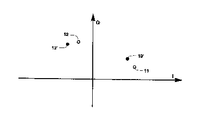
; It will be assumed that the signal vector has a
movable end at a first point 11 at a certaln time instant
~j~A which will be called a first time instant. In other words,
the signal vector has a first phase represented by the
5 first point 11 at the first time instant. At a second
time instant which is one symbol interval T later than
the first time instant, the signal vector has the movable
~' end at a second point 12 to have a second phase which
is 90 greater than the first phase if one of the symbols
10 represents the binary one during the one symbol lnterval
.~
under consideration. At a third time instant one symbol
3 interval T later than the second time instant, the signal
vector has the movable end again at the first point 11
to have a third phase which is equal to the first phase
15 and is 90 less than the second phase if anothex of the
symbols represents the binary zero between the second
and the third time instants. It should be noted that
the terms the "first phase" and the "second phase" are
ç used for the time being differently from those usèd on
20 describing the gist of this inventlon heretobefoxe.
At any rate, the movable end moves along a circular
locus having a center at the origin and a radium which
ls equal to the absolute value. The signal vector has
a phase variable 90 forwardly or counterclockwise and -
25 90 backwardly or clockwise when each symbol represents
the binary one and zero, respectively. It may be mentioned
.
'.
~ - 12 - 2~2~
.
x here that the modulating signal comprises a particular
symbol sequence or pattern comprising the symbols in a
predetermined manner and a data symbol sequence comprising
the symbols to represent data or information which is to
5 be transmitted to the recelver. The angular modulated
or the received signal comprises a particular signal
sequence and a data signal sequence which are produced
by the minimu~ phase shift keying modulatlon of the
carrier signal by the particular and the data symbol
10 sequences. The particular and the data signal sequences
are demodulated into reproductions of the particular and
the data symbol sequences ~y detecting a phase variation
in the phase of the signal vector in each symbo~ interval T.
The above holds only when the angular modulated signal
15 is quadrature demodulated by using a local (reference)
carrier signal having a local caxrier frequency which is
equal to the recelved carrier frequency. If the local
carrier signal has an actual carrier frequency which has
a frequency difference of a finite value relative to the
20 received carrier frequency, such first and second points
11 and 12 move forwardly and backwardly along the circular
locus when the finite value is positive and negative.
Angular frequencies will now be used as such
frequencies. The received carrier signal has a carrier
25 angular frequency W, denoted by a double-u rather than
the Greek omega minuscule. When su~jected to the minimum :
- 13 - 2 ~1 3 ~1
phase shift keying modulation, the modulated or the
received signal of a unit amplitude is represented by:
cos0(t) cosWt ~ sin~(t) sinWt,
- whexe cos~(t) and sin~(t) represent inphase and quadrature
S phase components of the modulated signal, respectively.
It will be presumed that the local carrier slgnal
- has a local-carrier angular frequency (W - w) and a phase
s offset ~ relative to the received carrier signal, where w
represents an angular frequency difference between the
` received carrier and the local-carrier angular frequencies.
Under the circumstances, the demodulated signal is given b~:
~, cos0(t~ cos(wt + ~) + sin~(t) ~ sin(wt ~ ~)
7 - cos~(t) sin(wt ~ ~) + sln~(t) cos(wt ~
It is now understood that the signal vector rotates
15 forwardly around the origin at an angular speed o
rotation of w radian per unit time in addition to a
rotation of 90 forwardl~ or backwardly per symbol
interval T and has a rotated phase different from the
' phase which is described above and will now be called
, 20 a reference phase for.discrimination from the rotated
i phase.
In Fig. 1, let the signal vector have the first
reference phase lllustrated by the first point 11 at
the first time instant as before. In other words, let
25 the signal vector have a first rotated phase which is
identical with the first reference phase. At the second
.
r. -: ...... . . . . ~ ,
.. ~ 14 ~ 2~3$~
;,
time instant, the second reference phase is given a
forward rotation of wT radian to become a second rotated
phase which is 90 plus wT radian greater than the first
reference phase and is represented by a different second -
point 12'. At the third time instant, the signal vector
has a third rotated phase into which the second rotated
phase is given a backward rotation of 90 minus wT radian.
The third rotated phase is therefore 2wT radian greater
than the first reference phase and is depicted at a
different third point 13'.
In this ~anner, the signal vector has a phase variable
either by wT radian plus 90~ or wT radian minus 90 per
symbol interval T. When the angular fre~uency difference
w is considerably large, it becomes impossible to correctly
reproduce the particular and the data symbol sequences from
the received signal.
Referring now to Fig. 2, the description will proceed
to a quadrature demodulating method according to a first
embodlment or aspect of this invention. The method is
20 applled in a receiver.to the quadrature demodulation ~ -
described above. The local carrier signal is either
regenerated from the received signal or locally generated
with an ordlnaxy precision. The local carrier signal
need not be phase synchronized with the received carrier
signal by ~he use of a phase synchronizing circuit.
In the manner described in the prior patent application,
- 15 - 2~2~
.
a sampling clock slgnal is generated i~ the receiver to
define a sampling interval which is substantially equal
... .
to the symbol interval T. The partlcular symbol sequence
or pattern has a pattern length N which is equal to the
~, 5 predetermined number of symbol intervals. The data symbol
sequence has a data length N'. It will be surmised that
~ .
the data length N' is preliminarily conveyed to the
receiver side and thst the local carrier frequency or
the local-carrier angular frequency is stable at least
throughout the pattern length N plus the data length N'.
The method starts when the receiver is supplied with
the angular modulated or the received signal. At a
first primary step 21 at which frequency difference
. .
determination starts, the particular signal sequencq is
quadrature demodulated by the local carrier signal into
a first vector signal representa~ive of a first signal
vector having a first phase variable in compliance with
¦ the predetermlned manner and the frequency difference.
¦ The first primary step 21 is therefore a quadratu~e
demodulating step of ~uadrature demodulating the angular
modulated or the received signal by the local carrier
signal into the first vector signal and into a second
vector signal representative of a second signal vector
having a second phase variable in compliance with the
data and the frequency difference.
At a second primary step 22, the sampling clock signai
k~ ,?~ r
- 16 - 202~
,................................. .
.~ is used to derive phase value ~(kT) from the first vector
signal, where k represents a time instant number or a
symbol count of the symbols in the particular symbol
, sequence and increases one by one at the symbol interval T.
,2 5 The phase values are variable from one to another in
,"~! compliance with the predetermined manner and the frequency
':
difference. In any event, the second primary step 22 is
.~ . .
¦ a converting step of converting the first phase to the
phase values substantially at the symbol interval T. -.
At a third primary step 23, a phase difference D ~ (k)
is calculated between two consecutive ones of the phase
values in the manner illustrated by a difference between
each phase value ~(kT~ and another phase value ~((k - l)T)
that is derived one symbol interval T before. The third ~.
lS primary step 23 is therefore a phase difference calculating . .
step of calculating the phase difference as a phase
variation in the first phase in each symbol inter~al T. ~
At a fourth primary step 24, the phase difference -
~(k) is compared with a reference variation a~(r) which
20 is determined by the predetermined manner and is equal to
~ plug 90, minus 90, and 0 when the particular symbol
f sequence consists of the symbols which consecutively :
, represent the binary one alone and the binary zero alone
f and alternatingly represent the binary one and zero,
25 respectively. The reference variation should be changed
in connection with partial sequences when the particular -
:
2 0 2 1 ~ 6 ~
? 17
.
,:
symbol sequence comprises such partial sequences. In this
manner, it is possible to determine an individual phase
I error E~(k) which is equal to the forward rotation o~ wT
- radian described in conjunction with Fig. 1. The fourth
5 primary step 24 is consequently an error calculating step
of calculating the individual error to provide a plurality
of individual errors substantially during the predetermined
number of symbol intervals NT. Being determined by the
predetermined manner, the reference variation ~ ~(r) is
10 preliminarily known at the receiver side.
At a fifth primary step 25, the individual error E~(k)
is summed up into a summation. At a sixth primary step 26,
the time instant number k is checked against the
~ predetermined number N. If the time instant number k is
¦ 15 less than the predetermined number N, one is added to the
time instant ~umber k. The sixth primary step 26 returns
, to the first primary step 21. It should therefore be
¦ unders~ood that the ~uadrature demodulating, the converting, ~-
¦ and the error calculating steps include the sixth primary
step 26.
When the time instant number k increase substantially
up to the predetermined number N, the sixth prlmary
step 26 proceeds to a seventh primary step 27 at wnicn
the summation is divided by the predeter~ined number N.
25 The seventh primary step 27 is accordingly an averaging
ste~p of averaging the individual errors into a phase
2~2~3~
- 18 -
... .
error E0 between the first phase and a first correct phase
which the first signal vector should have when the frequency
difference were equal to zero. The converting, the phase
difference calculating, the error calculating, and the
averaging steps may collectively be called an error
determining step of determining the phase error by
, . .
~;i comparison of the phase variation in the first phase
with the reference variation.
The seventh primary step 27 procees to a first
10 secondary step 31 at which the data signal sequence is -~
quadrature demodulated by the local carrier signal into
the second vector signal. At a second secondary step 32,
the second s~gnal vector is sampled by the sampling clock
signal into phase values ~(kT). At a third secondary
step 33, the second phase of each phase value is corrected
by the accumulated phase error kE~, in which the phase
error E~ is calculated in the seventh primary step 27,
into a second correct phase ~(kT) which each phase value
of the second phase would have when the frequency
difference wexe equal to zero. At a fourth secondary
step 34, the time instant number k is checked against
the data length N' or, more precisely, against a sym~ol
count in the data length N'. If the time instant number k
i9 less than the data length N', tne fourth secondary
s~ep 34 returns to tne first secondary step 31 with one
added to the time instant number k.
2~21~
., . 1 9
,
~ It is now understood that the quadrature dem~dulating
, ........................................................................ .
step is carried out at the first and the sixth primary
steps 21 and 26 and at the first and the fourth secondary
steps 31 and 34. The converting step is carried out at
the second primary and secondary steps 22 and 32. A
`~ combination of the third and the fourth secondary steps
.~. .
33 and 34 is a phase correcting step of correcting the
second phase into the second correct phase. When the
time instant n~mber k increases substantially up to the
10 data length N', the quadrature demodulating method comes
to an end.
D Referring now to Fig. 3, the description will proceed
to a quadrature demodulating device according to a second
embodiment or aspect of this invention. The device is
15 ~or carrying out the quadrature demodulating method
illustrated with reference to Fig. 2.
The demodulator comprises a local carrier generator 36 - ~-
for either regenerating from the received signal or locally -
generating a local carrier signal of a local carrier
20 frequency which has a.frequency difference relative to
the received carrier frequency. The received signal is
supplied to a quadrature demodulator 31 for quadrature
demodulating the received signal into inphase and
quadrature phase component signals I and Q representative
25 of inphase and quadrature phase amplitude values which -
are variable with time t and are cooperatively
:r . . r ~
, ~ .
~ - 20 - 2~2~3~
,,~ ..
representative of the first and the second signal vectors
described before.
A combination of the inphase and the quadrature phase
c,
- component signals is therefore the first and the second
vector signals when derived from the particular and the
data signal sequences. Derived from the particular signal
sequence, the inphase and the quadrature phase component
~ signals I and Q are delivered to a frequency difference
i~ determining or detecting circuit 38. The circult 38,
~ 10 which will presently be described, detects a phase error -~
¦ representing a frequency di~ference hetween the received
and local carrier signals. The inphase and the quadrature
phase component signals I and Q are also supplied to a
phase correcting circuit 39 operable in the manner which
will later be described.
Turning to Fig. 4, the frequency difference determining
circuit 38 comprises an orthogonal to polar coordinate
converter 41 for producing from the inphase and the
~uadrature phase component signals I and Q phase values
~(kT) which the first.signal vector has substantially at
the symbol interval T determined by the predetermined
manner and preliminarily known at the receiver side.
The orthogonal to polar coordinate converter 41 thereby
produces a phase value signal representative of the
phase values. It is readily possible to implement the
orthogonal to polar coordinate converter 41 by a read-
only memory ~ROM).
: ' . ' : . ! . ' '
- 21 - . 2~
. .
~he phase v~lue signal is delivered to a delay circuit
:
. 42 and a phase value subtracter 43. The delay circuit 42
........... gives a delay of one symbol interval T to each phase value
to produce a delayed signal representative of delayed
values, each given the delay. Supplied with the phase
.;~ value signal and the delayed signal~ the subtracter 43
, calculates a phase difference ~(k) between two consecutive
.~ ones of the phase values ~(kT) and ~((k - l)T). The phase
: difference ~(k) represents a phase variation to which the
.~ 10 first signal vector is subjected in each symbol interval T.
The subtracter 43 thereby produces a difference signal
representative of such phase differences. A combination
of the delay circuit 42 and the phase value subtracter 43
therefore serves as a phase dlfference calculating circuit
supplied with the phase value signal for calculatlng each
phase difference as the phase variation to produce the
difference signal.
The difference signal is delivered to a difference
~ . subtracter 44 which may be referred to simply as a
:~ 20 subtracter depending Qn the circumstances and is supplied
through a signal supply lead 45 with a reference signal
representative of plus 90, minus 90, or 0 at a time :-
as a referenc~ variation D 0 (r) in the phase values ~kT)
~ of the first signal vector. The subtracter 44 thereby
1 25 calculates an individual error E~)k) between the phase
difference ~(k) and the reference variation to produce
- 22 - 20~136~
... .
an error signal representative of such individual errors.
Each invididual error is equal to a difference between the
first phase of the first signal vector and a first correct
phase which the first signal vector would have when the
frequency difference were equal to zero. It should be
noted in this connection that the reference variation
is determined by the predetermined manner and is
preliminarily known at the receiver side and that tne
slgnal supply lead 45 is in practice a reference signal
generating arrangement for generating the reference
signal in the manner described in the prior patent
application.
The error slgnal is delivered to an averaging circuit
46 in which the individual errors are summed up into a
summation until the time lnstant number k of the individual
errors reaches a total number K wh~ch is substantially
equal to the predetermined number N and is determined by
the attendant in accordance with the predetermined number
in the manner described in the prior patent applicatlon.
The averaging circuit-46 calculates a phase error E~ by
dividing the summation by the total count K and supplies
a phase error signal lead 47 with a phase error signal
representative of the phase error E~.
Reviewing Figs. 3 and 4, it is understood that the
frequency difference detecting circuit 38 is for comparing
the phase variation in the first phase with the reference
- : ~r .
- 23 - 2921~1
"
variation (45). The frequency difference determining
circuit 38 thereby determines or calculates the phase
error E~ representative of a frequency difference
between the received carrier and local carrier signals,
~ .
~' 5 producing the phase error signal.
Referring to Fig. 5, the phase correcting circuit 39
comprises an orthogonal to polar coordinate converter S1
supplied with the inphase and the quadrature phase
comp~nent signals I and Q produced by the quadrature
demodulator 37 in response to the received signal. The
orthogonal to polar coordinate converter 51 produces a
radius vector signal R and an argument signal A. The
radius vector signal R xepresents the afore-mentioned
absolute value of the signal vector. The argument
signal A represents an argument of the radius vector,
namely, tne phase value ~(~T) of the signal vector. ~ -
The radius vector signal R is delivered directly -
¦ to a polar to orthogonal coordinate converter 52. The
j argument signal A is supplied to the polar to orthogonal
coordinate co~verter 52 th~ough a phase correction
subtracter 53 supplied with an accumutated phase error
slgnal from an accumulator 54. The accumulator
accumulates the phase error E~ supplied through the
phase error signal lead 47 from frequency difference
determining circuit 38 to produce the accumulated phase
. . .
error kE~. The subtracter 53 subtracts the accumulated
. '
:,:~,. . .
:
` - 24 - 2~21~1
S phase error kE~ from the phase value ~kT) xepresented
by the arugment signal A to provide a correct phase
value ~(kT) to produce a correct phase signal A
~ representative of the correct phase value.
^~ 5 Supplied with the radius vectox signal R and the
correct phase signal A, the polar to orthogonal coordinate
converter 52 converts a combination of the absolute value
of the signal vector and the correct phase value o~ the
signal vector from polar coordinates back to the orthogonal
coordinate system represen~ative of the phase plane.
The polar to orthogonal coordinate converter 52 thereby
produces correct inphase and quadrature phase component
signals I and Q representative of a corrected vector
signal, namely, the reproduced data sequence. It is
readily possible to implement each of the coordinate
converters 51 and 52 by a read-only memory (ROM). ;-
Tuxning to Fig. 6, the phase correcting circuit 39
may alternatively comprise cosine and sine read-only
memories (ROM) 56 and 57, both supplied with the
20 accumulated phase error signal from accumulator 54 which -
in turn is supplied with the phase error signal from the
frequency difference determining circuit 38 through the
phase error signal lead 47. The cosine read-only memory
56 produces a cosine signal representative of cos(kE~). -
The sine read-only memory 57 produces a sine signal
representative of sin(kB~).
: `
` - 25 - 2~2~
..`.
.~
It may be mentioned here that a correct sig~al vector
` has a correct phase ~(kT) which is equal to the phase ~(kTl
,
represented by the inphase and the quadrature phase
!j,, component signals I and Q minus the phase error kE~.
A correct inphase component of the correct signal vector
~ is therefore equal to Icos~kE~) minus Qsin(kE~), which
,`' may be called first inphase and quadrature phase parts.
,. .
~ A correct quadrature phase component of the correct signal
,i vector is equal to QcoslkE~) plus Isin(kE~), which may be
called second quadrature phase and inphase parts.
In view of the above, the cosine signal is delivered
~, to first inphase and quadrature phase multipliers 61I and
61Q which are supplied with the inphase and the quadrature
phase component signals I and Q produced by the quadrature
demodulator 37 ln response to the received signal. The
first inphase multiplier 61I produces a first inpyase
slgnal representative of the first inphase part. The
¦ first quadrature phase multiplier 61Q produces a ~irst
quadrature phase signal representative of the second
quadrature phase part..
The sine signal is delivered to second inphase and
quadrature phase multipliers 62I and 62Q which are supplied
with the inphase and the quadrature phase component signals
I and Q delivered to the first inphase and quadrature phase
multipllers 611 and 61Q. The second inphase multiplier 62I
produces a second inphase signal representative of the --
:i ~
' A 26
second inphase part. ~he second quadrature phase
'.!, .
multiplier 62Q produces a second quadrature phase signal
representative of the first quadrature phase part.
A subtracter 63 is supplied with the first inphase
signal and the second quadrature phase signal to produce
- .
a correct inphase component signal I representative of the
correct inphase component. An adder 64 is supplied with
the first quadrature phase signal and the second inphase
signal and produces a correct ~uadrature phase component
signal Q representative of the correct quadrature phase
component.
Further turnlng to Fig. 7, the phase correcting
circuit 39 is lmplemented by a read-only memory (ROM) 65 ~-~
and an accumulator 54 as a further alternativè. The read-
only memory 65 is supplied with the inphase and the
quadrature phase component signals I and Q produced by
the quadrature demodulator 37 in response to the received
signal. The read-only memory 65 is additionally supplied
with the accumulated phase error signal from the
accumulator 54 which in turn is supplled the phase error
signal from the frequency difference determining circuit
37 through the phase error signal lead 47. Using the
inphase and the ~uadrature phase component signals I and Q
and the accum~lated phase error signal correctively as
¦ 25 an address or access signal, the read-only memory 65
I produces the above-mentioned correct inphase and quadrature
-.,
3 6 ~ - -
- 27 -
,.',
-~ phase component signals I and Q. When each of the inphase
:.
~; and the quadrature phase component signals I and Q and
. the correct inphase and quadrature phase component signals
~` I and Q is rep~esented by M bits to represent each phase
s S value and when the accumulated phase error signal is
~x~ represented by a like number of bits in representing
each phase error kE~, where M represents a predetermlned
integer, the read-only memory 65 should have a memory
capacity of 2 M x M x 2 blts.
Reviewing Figs. 3 through 7, the phase error signal
may be used to stop operation of the phase correcting ~-
circuit 39 until it begins to represent the phase error E~.
In any event, the phase correcting circuit 39 is supplied
with the phase error signal representative of the phase
15 error E~ and the aforementioned second vector signal to ~ -
correct the second phase ~tkT) by the phase error E~ into
a second correct phase ~(kT) variable in compliance with
the data and the carrier frequency to produce the correct
inphase and ~adrature phase component signals I and ~
20 collectively as a corrected vector signal which has the
correct phase. It is possible to use a digital signal
processor in ~lace of the fre~uency difference determining
and the phase correcting circuits 38 and 39 exemplified
above. It is moreover possible to use a memory for -
temporarily remorizing the phase values for subsequent
processing in the manner which will later be described.
`~
2~2~
i - 28 -
~his is useful particularly when the symbols are represented
by bursts as in the time division multlple access
communication.
,. .
In Figs. 3 through 7, the phase error E~ represents
the frequency difference w between the received and local
,;
r' carrier signals. It is therefore possible to ~eed the
;
phase error signal back to the carrier generator 36
through a connection indicated by a dashed line 47' in
'i correcting the local carrier frequency.
In connection with Fig. 4, the orthogonal t~ polar
coordinate converter 41 will now be taken into consideration.
When implemented by a read-only memory, the converter 41
is not very co~pact. Its power consumption is not
negligible. It i5 therefore desirable to avoid us~ of
a read-only memory in obtaining the phase values ~(kT)
from the inphase and the quadrature phase componen~s,
which will now be denoted by I~t1 and Q(t).
Referring now to Fig. 8, an actual signal vector 66
is depicted on a phase plane which ls similar to that
illustrated with refer.ence to Fig. 1. The actual signal
vector 66 is derived by sampling the inphase and the
quadratuxe phase components I(t) and Q(t) by a sampling
clock signal of a sampling interval which is substantially
equal to the predetermined symbol interval T. Consequently,
the actual signal vector 66 is represented by actual
inphase and qudrature phase component samples I(A, kT) and
;; . r . ., , ~
~ .
~2~
~ - 29 _
,: :
.~ A(A, kT) and has an actua~ absolute value r(kT) and an
.~ actual phase value ~(A, kT). Such actual phase values
~. are variable substantially at the symbol interval T and
,~ will be called phase values of the first phase when the
actual signal vector 66 is derived from the particular
signal sequence as the first signal vector. It is
possible to understand that each phase value of the
~ first phase ~(A, kT) is represented by the actual inphase
.. and quadrature phase component samples I(A, kT) and
~- 10 Q(A, kT).
If subjected to quadrature demodulation by an ideal
local carrier signal a frequency equal to having the
received carrier frequency, the particular signal sequence
would become ideal inphase and quadrature phase component
signals. An ideal or zeroth signal vector 67 is thereby
defined to have ideal inphase and quadrature phase
component samples I(O, kT) and Q(O, kT), an ideal absolute
value ~(kT), and an ideal phase value ~(O, kT). Such
ideal phase values are defined in correspondence to the
respective phase values of the first phase and will
~, alternatively be called reference values. Inasmuch as ~:
the predetermined manner and the received carrier frequency
are preliminarily ~nown, i.t is possible to determined
each re~erence value ~O, kT) and to represent the
reference value by the ideal inphase and quadrature
phase component samples I(O, kT) and Q(I, kT).
: . . -, , i .- ,. ....
r.:, " . , , ~ ' ,, ; : . .
~2~
- 30 -
If given a backward or negative rotation of the
reference value ~(O, kT), the ideal signal vector 67
xests on the positive part of the inphase axis I. Let
the actual signal vector 66 be given the negative rotation.
The actual signal vector 66 becomes a rotated signal
vectox 68 which has rotated inphase and quadrature
~`:
~ component samples I(R, kT~ and Q(R, kT), the actual
, . . .
r' absolute value R(kT), and a rotated phase value ~(R, kT).
Such ro~ated phase values correspond to the respective
phase values o~ the first phase and will alternatively
be referred to simply as rotated values. Represented
~- by the rotated inphase and quadrature phase component
samples I(R, kT) and Q(R, k~), each rotated value ~(R, ~T)
;~
is equal to the phase value of the first phase ~(A~ kT)
minus the reference value ~O, kT) and is calculated in
accordance with:
( I(R, kT) ~
Q(R, kT) /
, I(O, kT) Q(O, kT) I~A, kT)
I = / R~kT). ~1)
- Q(O, kT). I(O, kT) Q(A, kT)
If the ideal local carrier signal were used, the
actual and the ideal signal vectors 66 and 67 would have
a common phase variation. The rotated value would therefore
be kept constant. In practice, the local carrier frequency
may not necessarily be equal to the received carrier
frequency. T~o consecutive ones of the rotated values
. ` ~
2~
~ ~ 3 1
r~ I
R, kT) and ~(R, (k - 1) T) therefore have a phase
` difference or phase variation ~(R, k~ which depends
on the predetermined manner and the carrier frequency
difference. On the other hand, two consecutive ones of
. 5 the reference values ~(R, kT) and ~(O, (k - l)T) have a
reference variation a~ k) which is determlned by the
predetermined manner and the recelved carrier frequency,
both preliminarily known.
difference between the phase difference or the
phase variation and the reference variation is calculated
to provide an individual error E~(k). Inasmuch as the
rotated or the actual absolute value at a symbol count k ; :.
is approximately equal to the rotated or the actual :
absolute value at the symbol count less one Ik - 1) and
, .. ... .
15 inasmuch as the individual error would be small so that -
the sine of the individual error is approximately equal
to the individ~al error, the individual error is calculated
according to:
E~(k) = ~I(R, ~(k - llT)Q~R, kT) :.
- I(R,.kT)Q~R, ((k - 1~T) ] :~
¦ /[I ~R, kT1 + Q2(R, kT)~ . ~2)
Referring to Fig. 9, the description will proceed
to a quadrature demodulating method according to a third
embodiment of this invention. The method being described, ~::
is a modificatlon o~ the method illustrated wlth reference
to Fig. 2.
~, i .'.: .
2~
~ 32 -
At a first step 71 which corresponds to the first
primary step 21 described in conjunction with Fig. 2,
the particular signal sequence is ~uadrature demodulated
. ~
into the first vector signal representative of the first
slgnal vector having the inphase and the quadrature phase
^
;~- components I~t) and Q(t). At a second step 72, the inphase
and the quadrature phase components are sampled into the
~; phase values of the first phase, namely, into the actual
-
inphase and quadrature phase component samples I(A, kT~
. 10 and Q(A, kT), substantially at the symbol interval T.
At a third step 73, the phase value of the first
phase is given the backward rotation. The rotated value
.
~(R, kT) is gi~en by a combination of the rotated inphase
and quadrature phase component samples ItR, kTJ and Q(R, kT)
which are calculated in accordance with Equation (1).
At a fourth step 74, the individual error E~(k) is
calculated according to Equ~tion (2). At a fifth step 75,
such individual errors are su~med up into a summation.
At a sixth step 76, the symbol count k is checked against
a total count K which is determined so as not to be
greater than the predetermined number determined ~y the
predetermined ~anner. Determination of the total count K
is described in the prior patent application and wlll not
, be described in detail herein.
I 25 I~ the symbol count k is less than the total count K,
I the sixth step 76 returns to the first step 71. When the
~ 33 ~ 2~ 61
.
~ symbol count reaches the total count in the sixth step 76,
.~,, .
` the summation is divided at a seventh step 77 by the total
count K to provide a phase error E~ between the first phase
and a first correct phase whlch the first signal vector
S would have when the carrier frequency difference were
~; equal to zero.
On quadrature demodulating the data signal sequence,
the seventh step 77 proceeds to the secondary steps
described in connection with ~ig. 2. When the frequency
difference w should be calculated, the summation is
divided by a product of 2~T and the total count K rather
than by the total count K aone. It is possible to deal
with the first through the seventh steps 71 to 77 by a
digital signal processor. The secondary steps can also
be dealt wlth by the digital signal processor.
Reviewing Fig. 9, it ls understood that a combination
of the first and the sixth steps 71 and 76 serves as a
quadrature demodulating step of demodulating the angular
modulated or the received signal into the first and the
¦ 20 second signal ~ectors~ Another combination of the second
through the se~enth steps 72 to 77 serves as a computing
step of computlng the phase error E~ between a phase
variation a~R~ k) in the first phase and a reference
variatlon a~(O, k) determined by the predetermined manner
and the receiv~d carrier frequency.
More partlcularly, the second and the sixth steps
34
c'
i`~ 72 and 76 collectively serve as a phase value calculatlng
- step of calculating the phase values of the first phase
I(A, kT) and Q~A, kT). The third and the sixth steps 73
and 76 collectively serve as a rotated value calculating
step of calculating the rotated values I(R, kT) and QtR, kT)
by using each of the phase values of the first phase and
the reference value I(O, kT) and Q(O, kT). The fourth
through the sixth steps 74 to 76 collectively serve as
an individual error calculating step of calculating the
individual error E~(k) by calculating the phase difference
~tR, k). The seventh step 77 sexves as a phase error
calculating step of calculzting the phase error E~.
Referring to ~ig. 10, the description will proceed
finally to a quadratue demodulating method according to a
fouxth embodiment of this invention. The method being
described, is another modification o~ the method illustrated
with reference to Fig. 2 and makes use of a memory which
is descrlbed reviewing ~igs. 3 through 7 and may be -
understood as represented by the block 38 in Fig. 3.
At a first step 8.1, the particular signal sequence
is quadrature modulated ~nto the first signal vector
represented by the inphase and the quadrature phase
components I(t) and Q~t). At a second step 82, the
inphase and the quadrature phase components are sampled
into the phase values of the first phase ln the manner
depicted by I(A, kT) and QtA, kT). The phase values are
.' ' ' :
~ ,
~`:
2~213~1
_ 35 _
~; stored in the memory as memorized values. At a third
i,............................................... .
step 83, the symbol count k is checked against the total
count K.
If the symbol count k is less than the total count K,
the third step 83 returns to the first step 81. When the
symbol count becomes equal to the total count, the phase
values of the first phase are memorized substantially
throughout the particular signal sequence. The third
step 83 proceeds to other steps which will be described
below.
At a fourth step 84, each memorized value is used
~ in calculating the rotated value ~(R, kT) in accordance
¦ with Equation ~ As before, the rotated value is
depicted by the rotated inphase and quadrature phase ~-
component samples I(R, kT) and Q(R, kT). Such rotated
values are buffered in the memory.
At a fifth step 85, two consecutive ones of the
rotated values ~R, kT) and ~l~, (k - 13T) are used in
calculating the individual exror E~(k) according to
Equation ~2). At a sixth step 86, the individual eerors
are summed up into the summation. At a seventh step 87,
the symbol count k is again checked against the total
count K.
If the sy~bol count k is less than the total count K,
the seventh stçp 87 returns to the fourth step 84. When
the symbol count reaches the total count, the phase error
''
..
. . . _ .
' - 36 - 2~2~
~. -
~-~ E~ is calculated at an eighth step 88.
,................................. .
On quadrature demodulating the data signal sequence,
the eighth step 88 proceeds to the secondary steps described
in conjunction with Fig. 2. The frequency dlfference w
can be calculated like in Fig. 9. It is possible to use
`7
?~,' a digital signal processor in dealing with the first through
~ the eighth steps 81 to 88 and furthermore in processing
,~ the secondary steps.
In Figs. 3 through 7, the phase error E~ xepresents
the frequency difference w between the received and local
carrier signals. It is therefore posslble to feed the
phase error signal back to the carrier generator 36
through a connection indicated by a dashed line 47' in
correcting the local carrier frequency. This feedback
15 operation will now be described referring to Figs. 11 ~-
to 14.
In Fig. 11, steps 131 to 134 correspond to the
secondary steps 31 to 34 in Fig. 2 and correct the local
carrler frequency to the received carrier frequency. At
~ 20 step 131, the phase error signal E~ is supplied from the
I frequency difference determining circuit 38 to a local
carrier generator 36a (see Fig. 12). Referring te~porarily ~
to Fig. 12, a ~uadrature demodulating device comprises a ~-
orthogonal demodulator (detector) 37, the frequency
difference determining circuit 38 and the local carriex
generator 36a. Since the carrier fre~uèncy difference is
- ....
'`'.".:
2 ~ 2 ~
.;
corrected at the local carrier generator 36a, the -
demodulating device need not have the phase correcting
circuit in the Fig. 3 circuit.
Returning to Fig. 11, at step 132, the local carrier
~ 5 frequency generated from the generator 36a is corrected
-$~ to be equal to the received carrier frequency. Thereafter,
a data sequence is received at step 133 and this operation
contin~es untail the data length reaches the count N'
Isee step 134).
In Fig. 13, the local carrier generator 36a is
composed of a voltage-controlled oscillator (VCO) 361,
a digital-to-analog (D/A) converter 362 and an accumulator
363. The accumulator 363 accumulates the phase error E~
which is an averaged phase error per symbol and calculated
at the frequency difference determining circuit 38. The
accumulated phase error is convexted into an analog value
by the D/A converter 362. In response to the converted
analog value, the VCO 361 changes its osc$11ation frequency,
i.e., the local carrier frequencyl so that the frequency
difference bet~een the received and local carrier
frequencies approaches to zero.
More specifically, since the VCO 631 has a control
voltage vs. oscillation frequency characteristic shown
in Fig. 14, if the local carrier frequency is higher than
the received o~e, a lower control voltage is applied to
the VCO 631 and vice versa. To avoid the _lvergent at
! ~ 2 ~ 2 1 ~ ~ ~
! - 38 -
.~ .
`~ VCo 631 and to shorten the VCO's convergent time, the
accumulator 363 performs the following weighting operation,
thereby to supply its output S(k) to the D/A converter 362.
S(k) - Wl ~ ~ E~ (i) + W E~(k~
where Wl and W~ are weighting factors.
It is to be noted that the above-mentioned accumulator
363 may be lmplemented by a digltal slgnal processor.
While thi~ lnvention has thus far been descri~ed in
specific conjunction with a few preferred embodiments
thereof, it will now be readily possible for one skilled
in the art to carry this invention into effect in various
other manners. For example, lt is possible to carry out
the method illustrated with reference to Fig. 2 by using -~
the memory lik~ the method descrlbed in connection with
Fig. 10 and by using the total count K described in
conjunction wi~h Figs. 9 and 10. The particular symbol
sequence is not restricted to those exemplified above.
If desired, it is readily possible to stop supply of
the inphase and the quadrature phase component signals
from the quadrature demodulator 37 to the frequency
difference determining circuit 38 as soon as the phase
error signal is produced. The memory can be used in
memorizing suc~essively the phase values of the first
and the second signal vectors and in buffering, when the
method is carrled out in accordance with Pig. 9 or 10,
. .
'I
2 ~
~- - 39 ~
,. :
the rotated values. As soon as the phase error E~ is
~: calculated at the seventh primary step 27, the fifth
:; step 75, or the sixth step 86, it is possible to begin
the third secondary step 33 described in conj~nction with
~,.
~' 5 Fi~. 2. .
.
~, .
.
'
'~
'
- ' ~