Note: Descriptions are shown in the official language in which they were submitted.
2;~
A-50034/PAD PROCESS FOR DEPOSITING OPTICAL THIN
FILMS ON BOTH PLANAR AND NON-PLANAR SUBSTRATES
__
I. Cross-Reference to Related Application
This is a continuation-in-part of allowed patent
application, Serial No. 154,177, filed February 8,
1988, entitled "MAGNETRON SPUTTERING APPARATUS AND
5 PROCESS".
II. Backaround of the Invention
The present invention relates to processes and
apparatus for high rate, uniform deposition and
formation of thin films, such as refractory metals
and/or oxides, nitrides, hydrides, carbides and
other compounds, mixtures, solutions and alloys of
such metals, and also to the deposition and
formation of composite films. Such films are formed
on planar and non-planar, concave and convex
substrates with a controlled thickness profile.
As used here, the term "controlled thickness profile"
refers to tailoring the thickness profile of a thin
film formed on a curved substrate from center to edge
to achieve a desired optical performance. The term
includes controlled varied thickness as well as
constant thickness.
~P~ 7
--2--
III. Description of the State of the
Conventional Technology
It is highly desirable to deposit optical quality
thin films on non-planar substrates such as
cylindrical and concave reflectors. However, it is
difficult to deposit thin films which are durable,
of high quality and of uniform thickness on what we
shall term "shaped" (i.e., non-planar, convex or
concave) substrates. Specifically, coatings
deposited at oblique incidence angles by conventional
evaporation methods tend to be soft and poorly
packed, resulting in low index of refraction and poor
film durability.
Masking is sometimes used to limit deposition angles
in such systems. See FIG. 16. Masking, however,
requires complicated chamber tooling and limits the
efficiency of such systems.
Thin films have been formed on a variety of
hemispheric-shaped and/or parabolic-shaped substrates
by gas scattering of thermally-evaporated materials.
Examples of commercial applications of the technology
include dental and surgical mirrors and the M-16 cold
mirrors depicted in FIGS. 15A and 15B. However,
coating materials such as ZnS/MgF2, not metal oxides,
are thought to be the materials of choice for the
thermal evaporation gas scattering process. Metal
oxides suffer from decreased film durability and
decreased deposition rates when formed using this
approach, as well as from reduced indices of
refraction, which requires more layers.
" ~
: ` . ~ ; !
` '
_3_ 2 ~
IV. Summary of the Invention
A. Obiects of the Invention
In view of the above discussion of the limitations of
the prior art, it is one primary object of the
present invention to provide a process for depositing
thin films of materials such as metal oxides and the
other exemplary materials listed in Section II above,
on shaped non-planar substrates, including concave
and convex substrates, without the problems normally
resulting from oblique incidence deposition and
without using substrate masking, and with associated
benefits such as durability and temperature
stability.
It is another, related object to form highly durable,
uniform, optical quality thin film coatings at high
rates on non-planar substrates.
It is still another related object to form such
coatings with a desired thickness uniformity or non-
unifor~ity, to provide optimum optical performance.
B. Characteristics of Deposition
and Reaction Zones
In one aspect, a fundamental difference between our
invention and the prior art is that with our
invention both deposition and reaction are effected
in long narrow axial zones adjacent the periphery of
a moving substrate carrier. According to this
aspect, our reaction is effected by a means of highly
intense plasma in a highly efficient manner at high
- .
:
--4--
reactive gas pressures in a long narrow zone,
isolated physically from the metal deposition zone by
a region of relatively low pressure. Through the use
of a reactive ion source configured to produce an
elongated uniform high intensity ion flux adjacent
the periphery of the carrier for generating an
intense reactive plasma from oxygen or other reactive
gas, such as the linear magnetron, or suitably
configured ion gun, the high pressure reactive volume
is substantially comprised of highly energetic gas
species, which greatly shortens the time required for
the reaction. Another advantage of this technique,
thus, is that the technique is not limited to
reactive gases such as oxygen. Rather, compounds can
be formed using less reactive gas species such as
nitrogen, hydrogen, gaseous oxides of carbon, etc.,
to form nitrides, hydrides, carbides, etc. The
invention overcomes all of the above-mentioned
disadvantages of the prior art and affords further
advantages in that considerable deposition speed
increases can be realized through the use of multiple
stations. The available reactive gas pressures and
deposition rates are well above the practically
attainable deposition rates using prior art
eguipment. Curved substrates can also be coated due
to the elimination of the requirement for tight
baffling.
In this application, we provide examples of
applications which highlight the practical value of
the fundamental differences between our invention and
the prior art.
'' ~ ,: , , - ,,, :- . -
C. Present System and Operation
In a presently preferred approach for forming thin
film coatings including refractory metal coatings and
optical quality dielectric coatings such as metal
oxide coatings, our invention uses a cylindrical
processing configuration in which substrates are
mounted on a rotating cylindrical drum carrier, or on
a rotating planetary gear carrier. The substrates are
moved past a set of processing stations comprising
(1) at least one sputtering device (e.g., a planar
magnetron or a CMAG rotating magnetron) operating in
a metal deposition mode for depositing silicon,
tantalum, etc., alternated with (2) preferably at
least one of a similar device such as a planar
magnetron operating in a reactive plasma mode, or an
ion gun or other ion source configured to produce an
elongated uniform high intensity ion flux adjacent
the periphery of the carrier, for generating an
intense reactive plasma, using oxygen or other
reactive gases including but not limited to nitrogen,
hydrogen or gaseous oxides of carbon. The
arrangement provides zones for both deposition and
reaction with complete physical separation of the
zone boundaries. When similar magnetron cathodes are
2S used, one is operated using a relatively low partial
pressure of the reactive gas (such as oxygen) to
provide the metal deposition mode while the other is
operated at a relatively higher reactive gas partial
pressure to generate the intense reactive plasma for
oxidation, etc.
The substrates and cathodes may be located inside or
outside (or both) the drum. Also, the arrangement is
2~ ~ 3~'~
6--
scalable in that a multiple number of cathodes/ion
guns can be used in each processing station set to
increase the deposition rates and the number of
materials formed. Various processing station
arrangements can be provided in a chamber and
operated separately, sequentially or simultaneously
for depositing and, e.g., oxidizing different metals.
As one example, four stations can be selectively
arranged and operated to perform the sequence
tantalum deposition, oxidation, silicon deposition
and oxidation, to quickly form alternating layers of
Ta2O5 and sio2.
In our process, the relationship between the power of
the deposition cathodes and the speed of rotation or
translation of the substrate can be tailored so that
in each pass, a deposited thickness of one or more
atomic layers can be obtained. By adding additional
cathodes of other materials, and by adjusting the
power to each cathode, effectively alloys can be
created of any desired ratio. For example, NiCr can
be formed in any desired ratio from cathodes of Ni
and Cr, over large areas, simply by adjusting the
relative power to the cathodes. By adding oxidation
stations, one can form complex oxides such as barium
copper yttrium oxide, forms of which are known to be
superconducting.
D. Summation of Certain Practical
Advantages of the Present System
The cylindrical rotating geometry used in our
sputtering system combined with the sputter
deposition stations and reactive plasma stations
provide fast, uniform deposition of optical quality
-7- ~ $ 7 ~:
coatings on large volumes of both flat and curved
parts. Parts such as tubes or polygons can be
coated uniformly around the entire periphery thereof
by incorporating a double rotating, planetary gear
mounting arrangement. Additionally, we have
deposited uniform coatings onto complex shapes such
as lamp glass envelopes. The efficiency of the metal
mode deposition in providing high deposition rates
for a given power input coupled with the spreading of
the deposit and heat over a large number of
substrates/large drum surface area provides a unique
combination of high deposition rates and low
substrate heating which permits the high rate
formation of coatings on even plastics and other low
melting temperature materials.
To provide a basis for comparison, conventional DC
reactive oxide sputtering processes provide oxidation
rates < 10 Angstroms/second off the target, while our
process provides instantaneous formation rates of
20 about 100-150 Angstroms/second for Ta205 and about
100 Angstroms/second for SiO2.
In one-specific aspect, our invention eliminates a
major difficulty associated with the prior art vacuum
deposition of multilayer and single layer thin films
on spherical, curved and non-uniform, unconventional
shaped substrates, by using controlled process
parameters to reproducibly form on such substrates
durable, high-quality coatings having controlled
thickness profiles of selected uniform or variable
thickness. Previously, various techniques have been
used in attempts to overcome the difficulties in
achieving controlled deposition on curved and flat
surfaces.
-8- 2~2 3 ~`7
For example, previously, attempts have been made to
solve uniformity problems using ei.ther double or
triple rotation of the substrate coupled with
introducing an inert gas to "scatter" the cloud of
depositing material. Masking techniques have been
used which shadow high vapor incidence regions in an
attempt to match the vapor incidence rate there to
low rate regions. Also, durability problems
associated with the oblique incidence deposition on
curved surfaces have been eliminated by masking such
regions.
However, these scattering and masking stxategies have
significant difficulties. As mentioned above,
scattering is used primarily for materials such as
ZnS/MgF2, which produce soft coatings with poor
abrasion and temperature durability. Hard coating
materials such as metal oxides, when thermalized,
suffer from reduced indices of refraction and poor
film durability.when made using the gas scattering
evaporation process. Masking increases coating
chamber tooling complexity, especially for curved
surface-s and complex curved surfaces such as bulbs,
and reduces deposition rates.
As suggested above, our invention overcomes these
problems by using a simple axial rotary motion
coupled with our high rate reactive sputtering
scheme. Axial rotation produces uniformity along the
equatorial axis and the inherent high pressures
associated with sputtering provides a gas scattering
effect for polar uniformity. The higher energies of
the sputtered atoms are sufficient to overcome the
thermalizing effects of the gas scattering and,
2~2~
g
consequently, form films of materials such as metal
oxide exhibiting good durability. High rates are
achieved by using the unique reactive sputtering
scheme described above in which the substrates such
as (but not limited to) bulbs are rotated
alternately through a high rate metallic sputtering
zone and an energetic reactive plasma. This
combination of rotating cylindrical geometry, and
sputter deposition and reaction technology
(presently, planar magnetron and reactive plasma
technology) accomplishes the desired result:
providing reproducible, highly durable, optical thin
film coatings deposited at high rates and with
controlled uniformity on a large surface area and/or
a large number of flat or spherical or other curved
substrates, including unconventional substrates
formed to a complex curvature and/or formed of low
melting point materials.
It is emphasized that, as used here in reference to
the present invention, phrases such as "controlled
thickness profile" or "controlled uniformity" imply
not only the ability to deposit coatings of precisely
constant thickness on flat or curved surfaces, but
also the ability to vary in a controlled fashion the
thickness of a coating deposited along a curved
surface, to achieve desired design objectives such as
spectral performance. Because it is an inherent
property of optical thin films to shift to shorter
wavelengths at higher incidence angles and because a
variety of incident angles exist across the surface
of a shaped substrate, the coating must be tailored
in such a way as to balance the spectral performance
across the reflector surface. For example, in the
case of the MR-16 reflection depicted schematically
.
:
: . :. :.
2 ~ t',~
--10--
in FIGS. 15A and 15B, the incident angles at the
center of the reflector are approximately 10 while
those at the edge of the reflector can be as large
as 53. A uniform thin film will shift optical
thickness approximately 5% to shorter wavelengths
(relative to incidence at 10). Using our process,
we are able to deliberately grade the thickness
uniformity across the MR-16 reflector, and to provide
a coating thickness which is about five percent
thicker at the edge than at the center, to balance
the spectral performance and make the light
projection uniform.
V. Brief Description of the Drawin~s
The above and other aspects of the invention are
described with respect to the drawings in which:
FIGS. l and 2 are, respectively, a simplified
schematic perspective view and a simplified schematic
horizontal se~tional view, both of a single-
rotational cylindrical drum magnetron-enhanced vacuum
sputtering system which embodies the principles of
our present invention;
FIG. 3 is a simplified schematic perspective view of
a double-rotational, cylindrical drum embodiment of a
magnetron-enhanced vacuum sputtering system which
embodies the principles of the present invention;
FIGS. 4 and 5 are, respectively, a simplified
sch~matic perspective view, partially cut away, and a
simplified schematic horizontal cross-sectional view
of one type of DC linear magnetron sputtering device
2~
--11--
useful in the ma~netron-enhanced vacuum sputtering
system of the present invention;
FIGS. 6 and 7 are, respectively, an exploded
perspective view and an end view, partly in
schematic, of one embodiment of a linear magnetron
ion source useful in the magnetron-enhanced vacuum
sputtering system of the present invention;
FIG. 8 is a simplified schematic horizontal sectional
view of an alternative rotational cylindrical drum
embodiment of our system;
FIGS. 9-14 depict one or both the transmittance and
reflectance curves for (a) optical quality films
deposited on curved glass mirrors (FIG. 9), glass
eyeglass lenses (FIG. 10), plastic eyeglass lenses
(FIG. 11), and for (b) anti-reflective coatings on
plastic (FIG. 12), yellow headlamp filter coatings
(FIG. 13), and mirror coatings on infrared radiant
heating lamps (FIG. 14);
FIG. 15A and 15B are, respectively, a schematized
perspective view and a vertical section view of a
deep dish glass lamp reflector on which reflected
multi-layer oxide coatings having the transmittance
characteristics evidenced in FIG. 9 were formed using
our present invention;
FIG. 16 schematically depicts the prior art
Martin/Rancourt technique for masking convex
substrates to preclude oblique incidence deposition;
-
- ,, :: . .
-. -; , - :;
.
,
: -: .. ,. ~:
~Q~ ~t~ ~
-12-
FIG. 17 schematically depicts the process of
depositing a thin film on a cylindrical glass bulb
using the double rotational scheme of FIG. 3;
FIGS. 18A and 18B schematically depict target to
substrate distances for, respectively, the center and
edge of a planar, concave, or shallow convex
substrate;
FIG. 19 depicts a thickness profile associated with
the concave substrate of FIGS. 18A and 18B;
FIG. 20 depicts a graph of target power as a function
of substrate position which is used to effect the
uniform thickness profile depicted in FIG. 21, or
other selected thickness profiles for planar,
concave, or shallow convex substrates;
FIGS. 22A and 22B schematically depict target to
substrate distances for, respectively, the center and
edge of a convex substrate;
FIG. 23 schematically depicts a thickness profile
associated with the convex substrate of FIGS. 22A and
22B; and
FIG. 24 depicts a graph of target power as a function
of substrate position which is used to effect the
uniform thickness profile of FIG. 25, or other
selected thickness profiles for convex substrates.
2~ 3~7
-13-
VI. Description of the Preferred Embodiment(s)
A. Sinqle and Double Rotation Rotary System
In one aspect, our present invention combines linear
DC magnetron sputtering cathodes operating in a
partial pressure separation regime and rotary
cylindrical workpiece transport to provide a sputter
deposition system which is capable of high rate
formation of single or multi-layer optical films of
materials such as, but not limited to, sio2, Tio2 and
Ta205. This combination is achieved despite the
previous incompatibility of linear magnetron
sputterers and rotary workpiece transport and despite
the inherent difficulty (as evidenced in the prior
art) in implementing partial pressure separation.
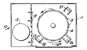
FIGS. l and 2, respectively, depict a simplified
schematic perspective view and a horizontal sectional
view of a single rotation embodiment of our
magnetron-enhanced vacuum sputtering system. The
illustrated sputtering system 10 comprises a housing
11 which forms a vacuum processing chamber and is
connect~d to a suitable vacuum pumping system 12
shown in FIG. 2. The vacuum pumping system includes
a cryopump or other suitable vacuum pump or
combinations thereof for exhausting and pumping down
the vacuum chamber via exhaust port 13. The system
10 also includes a cage-like drum 14 which is mounted
for rotation about shaft 16 and has a cylindrical
side which is adapted for mounting substrates 15 of
various configurations and sizes. The substrates 15
can be mounted directly on the drum 14, facing
outwardly toward sputtering stations which are
spaced ahout the external periphery of the drum or
~. . ,;
,
-14-
facing inwardly toward sputtering stations spaced
along the internal periphery of the drum.
Alternatively, and referring to FIG. 3, the system lo
may incorporate one or more double rotational motion
mountiny arrangements 25, either in conjunction with
or as a replacement for the drum 14. The illustrated
planetary gear arrangements can be provided on the
drum alone or in combination with the single rotation
substrate mounting positions 15. The planetary gear
arrangement mounts and imparts double rotational
motion to articles such as tubes 18. The planetary
gear system 25 may comprise a sun gear 19 which is
driven by shaft 16. Alone or in conjunction with a
ring gear (not shown), the sun gear 19 rotates the
associated planet gears 21 about their own
rotational axes 21A as well as about the sun gear's
rotational axis 16A. In the illustrated embodiment,
the planet gear 21 is operatively connected to a
train of gears 22 which are mounted on shafts for
rotation about their axes 22A. The tubes 18 are
mounted on and rotate with the planet gear support
shafts about axes 22A. As a consequence of this
planetary gear mounting arrangement, rotation of
drum 14 and sun gear 19 along reversible path 16B
25 about axis 16A rotates planet gears 21 along path 21B
about axis 21A, ~hich is converted by the gear train
into alternating rotation of tubes 18 along paths 18B
about axes 22A. This double rotary motion of the sun
gear 19 and the planetary gears 21 enhances the
ability to coat articles such as tubes uniformly
about their entire circumference.
Referring further to FIGS. 1-3, in the illustrated
embodiment, a plurality of magnetron-enhanced
-~ ~
2~ 3$'~
-15-
sputtering devices, designated generally by the
reference numeral 30, are positioned about the outer
periphery of the drum 14. In one exemplary
embodiment, the station designated 26 is used to
deposit material such as silicon whereas station 27
deposits a different material such as tantalum and
station 28 is used to react a gas such as oxygen with
the substrates to convert the deposited metal
layer(s) to oxide. Thus, by rotating the drum 14 and
selectively operating the sputtering and reaction
stations 26, 27 and 28, the metals and/or oxides
thereof can be selectively formed on the substrate in
essentially any desired combination. For example, by
rotating drum 14 and sequentially activating the
cathodes sequence 26 and 27, while continuously
operating cathode 28, system 10 can form a silicon
layer a few atoms thick and oxidize the silicon to
SiO2, then deposit a layer of tantalum a few atoms
thick and oxidize the tantalum to Ta2O5. This
sequence can be repeated and altered as required to
form a composite optical coating of layers of SiO2
and Ta2O5 of precisely controlled thicknesses. It
should be noted that oxidation stations 30 such as
- the one at station location 28 can use a planar
magnetron cathode similar to deposition stations 26
and 27, by substituting oxygen for the argon; or can
use other ion sources capable of generating a
reactive ionized plasma, such as ion guns or the
linear magnetron ion source described in FIGS. 6 and
7, or other devices which generate the required
reactive DC or RF plasma.
. -
-16-
B. DC Magnetron Sputter (and Reaction~ Devices
FIGS. 4 and 5 schematically illustrate one type of DC
magnetron sputtering device 30 which is commercially
available from VacTec or other suppliers and can be
used at station locations 26 and 27 and, optionally,
at station 28, FIGS. 1 and 2. The sputtering device
30 comprises a housing which mounts a cathode 31 and
forms a front, reactive gas baffle 32 having an
opening 36 which is selectively closed by a shutter
(not shown). Cathode 31 is connected to a power
supply 33 for applying a voltage of, e.g, -400 v. to
-600 v. to the cathode relative to the baffle 32,
which is at anode potential (usually ground).
Permanent magnets (not shown) are mounted within the
cathode body for supplying a magnetic field B of
rectangular racetrack configuration along the
surface of the target 34 and perpendicular to the
applied electric field. Manifold tubes 37 are
situated adjacent the target 34 and are connected to
a source of gas for supplying reactive gas such as
oxygen or an inert working gas such as argon to the
sputter chamber defined by baffle 32 and target 34.
The device is cooled by water which is supplied via
inlet 38 and circulated to an outlet (not shown).
The baffles 32 in the individual sputter devices 30
effectively divide the overall processing cham~er 10,
FIGS. 1 and 2, into different regions or sub-chambers
at each sputterer in which different gas atmospheres
and/or gas partial pressures can be established.
Improvements could be readily implemented where one
or more additional pumps could be placed to improve
separation between regions of reactive and
non-reactive gases.
. .
3 ~ ~
-17-
Compounds, etc., such as oxide dielectric films can
be formed using the linear magnetron sputter devices
30 at the sputter stations 26 and/or 27 and using a
different type of device, such as the ion source 40,
FIGS. 6 and 7, which is described in the next
section, at reaction station(s) 28. Alternatively,
one can use at least two baffled linear magnetron
sputter devices 30 at the sputter stations 26 and/or
27 and at the reaction station 28. In both cases,
the sputter device and the ion source device are
enclosed in distinct partial pressure regimes or
chamber regions between which the substrate is
alternated by the continuously rotating drum. When
baffled magnetron cathodes 30 are used both to
sputter and to oxidize, the cathodes are operated at
relatively high power density in an oxygen ambient
within chamber 10 using a target designed for
sputtering the selected metal such as silicon or
tantalum. However, the baffle-separated magnetron
cathodes which are used at stations 26 and 27 for
metal deposition are operated in a low reactive gas
(oxygen) partial pressure environment for operating
in a metal mode and depositing metal at
consequentially high rates. The low oxygen partial
pressure is supplied by flowing inert working gas
such as argon into the chamber area via manifolds 37.
The other type of baffled magnetron cathode 28 is
operated at relatively higher reactive gas partial
pressure and sputter deposits the metal at a much
lower rate on the moving substrates but oxidizes the
metal at a much higher rate. The lower rate target
adds little to the overall deposition rate and thus
does not affect control, but does produce a highly
reactive plasma which allows the chamber oxygen to
:,
:' '
d
-18-
readily react with the growing thin film and, as a
result, permits the use of a relatively low overall
chamber oxygen partial pressure, which enhances
cathode stability and rate. This reactive sputtering
approach provides repeatable thin films deposited at
high rates, fully oxidized and with good optical
qualities.
C. Linear Maanetron Ion Source
FIGS. 6 and 7 depict a presently preferred embodiment
of a linear magnetron ion source 40 which can be used
at reaction station(s) 28, FIGS. 1 and 2 to provide
the desired narrow elongated reaction zone. The
linear magnetron ion source 40 uses electrons
associated with the sputtering plasma to generate
ions from a reactive gas in a separate local plasma.
These ions bombard the sputter-deposited material on
the substrates and thus form compounds with the
sputtered material. The ion source 40 can use the
cathode assembly 31 and the housing 32 shown in FIGS.
4 and 5 (for clarity, housing 32 is deleted in FIGS.
6 and 7). As adapted f~r use as a linear magnetron
ion source, direct-cooled cathode 31 includes an
O-ring seal 41 and tapped holes 42 in the face to
insulatingly mount a non-magnetic stainless steel
cover plate 43 in place of target 34 to seal water
circulation channel 45 in the cathode body. As
mentioned previously, cathode 31 also incorporates
permanent magnets (not shown) which provide a
magnetic field B of elongated rectangular "race
track" configuration 44 along plate 43 when the plate
is assembled to the cathode.
.. . ..
: ::
,
3 ~ ~
--19--
The ion source 40 is mounted adjacent the periphery
of the rotatable substrate carrier 14 with its long
direction or axis 4OL parallel to axis 16A of the
carrier 14, FIG. 1, and the width or short axis 40W
parallel to the circumference and the direction of
rotation 16B, FIG. 3, of the carrier.
A pair of stainless steel bar anodes 46-46 are
mounted along the elongated opposite sides of the
magnetron race track 44 on posts 47 which themselves
are mounted to the non-magnetic plate. The anodes 46
are insulated from the posts 47 and plate 43 by
stepped insulator stand-offs 48 having relatively
small sections which extend into holes 49 in the bar
anodes 46 and larger bottom sections which serve to
precisely space the anodes from the stainless steel
plate 43, as shown in FIG. 7. For mowlting, the
posts 47 are inserted through the stand-offs 48 and
through the holes 49 in the bar anodes 46, and are
secured by nuts 51.
Each anode 46 is a straight bar which is slightly
shorter than the long side of the magnetron race
track 4-4. Each anode's curved, generally cylindrical
outer-facing surface 52 conforms closely to the shape
of the magnetic field lines, B, FIG. 7. The anodes
46 are connected through wire leads 53 to a
conventional power supply 54 capable of providing
several amps current at, for example, +50 volts to
+140 volts bias. Preferably, insulating beads 56 (or
other suitable insulation) are mounted along the
section of the leads 53 within the housing to isolate
the leads from the plasma and prevent discharge at
the wire. Typical operation is at 2 to 4 amps and
,
-20- 2~
100 to 120 volts for a nominally twenty inch long
magnetron cathode.
As mentioned, the mounting location or station of the
linear magnetron ion source 40 is outside the
sputtering region(s) 26 or 27 but within the
associated plasma, which extends essentially
throughout the vacuum sputtering chamber. In
operation, the power supply 54 is used to maintain
the stainless steel bar anodes 46 at a positive DC
10 voltage of, for example, 100 to 120 volts relative to
the cathode 31 and the stainless steel plate 43,
which are at system ground and at an even greater
positive potential with respect to electrons in the
surrounding plasma. As shown most clearly in FIG. 7,
the curved surfaces 52 of the anodes provide electric
field lines E which are substantially perpendicular
to the magnetic field lines B. Electrons in the
associated plasma are accelerated towards the
positive anodes 46 and are trapped or confined by the
resultant E x B field along the magnetron race track,
greatly enhancing the probability of collisions with
the reactant gas supplied via adjacent inlet
manifolds 57, and thereby generating an intense
plasma defined by the race track configuration 44.
That intense plasma generates many ions from the
reactant gas which are accelerated away from the
anodes 46 by the potential gradient existing between
the anodes and the background plasma and toward the
substrates to enhance the reaction process, e.g., to
enhance oxidation of sputtered metals using oxygen as
the reactant gas.
In short, during operation, the elongated inverse
linear magnetron ion source 40 provides an intense
, ,~
' ' ~ ' ' ' ~ . ,' " ' ' ,
~'' ' .
-21-
long narrow reaction zone defined by the magnetron
race traek 44 having the long dimension thereof
spanning substantially the height of the substrate
earrier drum 14 and the narrow dimension thereof
defined along the eireumference of the earrier
parallel to the direction of rotation. In distinct
contrast to the prior art's requirement that
substantially the entire volume outside the single
sputtering zone be used for oxidation, in the current
version, our ion source 40 has a reaction zone which
is only about approximately five to six inches wide
and oceupies a small fraction of the eircumference of
the 29 inch diameter drum 14 (5"/~ D = 5"/91" =
5.5%), yet due to the intense magnetie field~enhanced
plasma reaction, completely oxidizes the deposited
thin film in, typically, a single pass. The small
ion souree cathode size and the fast reaction rate
provide unigue upward scaling capability, enabling
the use of a multiple number of sputtering cathodes
and oxidation reaction eathodes to provide hig~ rate,
high volume, high throughput deposition and
versatility in the seleetion of the composition of
the deposited eoatings.
The eombination of the rotatable drum and baffled
magnetron-enhaneed sputtering and reaetion eathodes
has provided high rate, preeisely controllable
optieal quality metal and dielectric layers in
thieknesses whieh are sealable, on both flat, eurved
and irregularly shaped substrates with a minimum of
masking. Also, because a given layer is built up by
a multiplieity of eoating passes, the effects of
eathode ares are greatly deereased sinee any sueh arc
represents only a portion of the eoating.
Additionally, when operating in the metal mode,
2~2~
-22-
magnetron arcs are t~pically less frequent and
intense.
The process described above involves sputtering metal
materials such as, but not limited to, silicon,
tantalum, titanium, iron or any other sputterable
material that forms stable oxides in an atmosphere
that permits the target to operate in the metal mode,
characterized by the highest rate of sputtering,
while elsewhere in the machine establishing an ion
process which preferably uses magnetron-enhanced
sputtering to expose the freshly deposited film to a
reactive atmosphere that converts it to an oxide.
The metal preferably is deposited no more than a few
atoms thick in order that the oxidation during the
subsequent reaction process is complete. Typically,
the drum 14 is rotated through the spatially
sequenced sputtering and reaction zones and the
process of sputter deposition, oxidation, sputter
deposition, oxidation is repeated as required to
build up the oxide layer to the desired thickness of
material such as SiO2. Then if a different layer
such as Ta2O5 is to be formed the same repetitive
process is repeated. Quite obviously, various oxide
forming cycles and metal deposition cycles can be
applied as required to form composites of oxides
alone, oxides and metals, or metal(s) alone.
As mentioned above, a locally intense ionized
reactive plasma from an ion source such as an ion gun
or a planar magnetron is used to provide the
oxidizing reaction. The uniformity of the magnetron
sputter-deposited metal films is precise, and the
cylindrical geometry allows uniform distribution of
sputtering materials. Thus, it is possible to use
s~;~
-23-
time and power control of the process in almost any
width or length of cathode, thereby overcoming the
historical problems of controllability, scalability
and throughput associated with conventional DC
magnetron reactive processes. As demonstrated in the
examples below, this ability permits precision
deposition of fractional optical layers such as one-
sixteenth visible wavelength optical layers which are
difficult to deposit using conventional vacuum
evaporation processes.
D. Alternative RotarY Cylindrical SYstems
FIG. 8 depicts an alternative sputtering system 60
which comprises a pair of cryopumps 12-12 situated on
opposite sides of the vacuum sputtering chamber, a
plurality of silicon sputtering devices 26 and
tantalum sputtering cathodes 27 formed on the inside
of the drum 14 facing outwardly and interspersed
oxidizing devices 28 situated on the outside of the
rotating drum 14 facing inwardly. The illustrated
system incorporates a planetary gear substrate
mounting and drive arrangement 25 for uniformly
exposing the periphery of work pieces such as tubes
to both the internal and external sputtering
stations. By virtue of this arrangement, and the
multiple silicon, tantalum and oxygen cathodes, the
silicon and tantalum layers and the oxidation of said
layers can be done at a high rate on a large number
of substrates. For example, a composite layer
comprising sio2 and Ta205 can be formed by operating
the silicon cathodes 26 simultaneously with the upper
right oxygen cathode 28, followed by operating all of
the tantalum cathodes 27 simultaneously with the
lower left oxygen cathode 28.
-24-
In still another application, the drum used in thepreviously described cylindrical sputtering system
can incorporate tooling that flips or rotates
substrates during a run to extend the capacity of the
coating machine. The possibilities include the use
of parallel banks or faces of substrates which are
rotated 180 to present substrates in each bank to
the sputtering stations or separate drums or
multiple-sided support bodies which are, for example,
of triangular or other polygonal cross-section and
are rotated by a planetary gear arrangement to
present the faces or the entire circumference to
selected sputtering stations. Also, the supports can
be mounted about an axis parallel to the drum axis
for rotation under computer control to selectively
present substrates to the work stations.
E. Controlled Coating Thickness Profiles
On Planar and Non-Planar Substrates
As described above and evidenced in several of the
following examples, our sputtering invention can
provide a constant coating thickness along flat
substrate surfaces and curved substrate surfaces,
including both convex and concave topographies.
Furthermore, the ability to precisely control the
coating thickness encompasses the selective variation
of coating thickness along both flat and curved
substrate surfaces. As evidenced below our process
forms durable optical quality oxide thin films and
other thin films on highly curved substrates at high
formation rates (currently at an instantaneous rate
of 100 - 150 Angstroms/second at the target) and with
optical properties (characterized, e.g., by
-25- ~f'~
reflectance and transmittance) closely similar to
those obtained on a flat substrate.
1. Convex-Shaped Substrates
As mentioned in the Backaround of the Invention, when
using prlor art optical coating technology, it has
been difficult to deposit on "shaped", convex
substrates, such as cylinders, optical quality thin
films which are durable, of high quality and of
uniform thickness. Specifically, coatings deposited
at oblique incidence angles by conventional
evaporation methods tend to be soft and poorly packed
and to have reduced optical properties.
As depicted schematically in FIG. 16, masking has
been used to limit deposition angles in such systems.
In the illustrated, exemplary prior art system, an
axial mask 70 is positioned closely adjacent to a
cylindrical substrate 13, between the source and the
substrate, to limit deposition to low angles
(typically 30 max.) and thus prevent the poor
quality films provided by deposition at higher angles
(30 < e < soo ) . However, masking decreases
deposition and throughput and requires complicated
tooling.
Our invention permits thin film deposition on convex-
shaped substrates, including cylinders, without the
problems associated with oblique incidence deposition
and without the need to use substrate masking and
associated complex chamber tooling to eliminate such
problems. More specifically, our process
accomplishes the heretofore unattainable goal of
forming highly durable, uniform, optical quality thin
,
-26-
film coatings at high rates on cylindrical and other
convex-shaped substrates.
Our process overcomes the problems of oblique
incidence deposition by using the above-described
simple axial rotary substrate motion and high rate
reactive sputtering scheme (FIGS. 1-3). More
specifically, our process accomplishes the heretofore
unattainable goal of forming highly durable, uniform,
optical quality thin film coatings at high rates on
cylindrical substrates and other convex-shaped
substrates without masking. The inherently high
pressure of about 1-5 mT at target-to-substrate
distances of about 5-20 cm associated with the
sputtering process provides multiple collisions per
particle, resulting in a high degree of gas
scattering, which enables the necessary uniformity
along the polar axis 16P, FIG. 3. At the same time,
the high sputtered particle energies of about 10 eV
which are inherent to our process reduce gas
scattering somewhat and provide good durability while
retaining the advantages of gas scattering.
Moreover, the combination of this reactive, omni-
directional sputtering process with the double
rotary-motion sputtering scheme depicted in FIG. 3,
enables uniform deposition 360 about the equatorial
axis 16E. The use of an axially elongated sputtering
deposition source such as (but not limited to) the
linear magnetron sputter source, FIG. 5, adapts the
sputtering scheme to elongated substrates such as the
cylindrical glass tubes 18, FIG. 3.
The ability to uniformly coat substrates which are
curved in three dimensions and to coat over 360 is
-27-
illustrated schematically in FIG. 17 for cylindrical
glass bulbs 18. Specifically, the use of the double-
rotary motion sputtering scheme depicted in FIG. 3 in
combination with the omni-directional uniform
deposition which is inherent to our high pressure,
high energy reactive sputtering approach forms a
coating over the entire bulb 18, including the curved
ends.
Also, high deposition rates are achieved by the
unique reactive sputtering scheme depicted in the
above-discussed FIG. 3, in which substrates such as
cylindrical glass bulbs 18 are alternated at a high
rate of speed between (1) the high rate metallic
sputter zone(s)26, 27 (FIG. 1), which form a coating
a few monolayers thick -- typically 2-5 Angstroms--
on the substrate, and (2) the energetic reactive
plasma zone(s) 28 (FIG. 1), which effects selected
reactions such as oxidation, nitridation, etc., and
has the capability to completely convert the
thickness of the deposited film to an oxide,
nitride, etc.
. In shQrt, our process overcomes the problems
associated with oblique incidence vapor deposition
using relatively simple tooling and without the use
of masks, and forms highly durable, uniform, optical
quality metal oxide and reacted metal compound thin
films at high rates on convex substrates.
2. Concave-Shaped Substrates
Our process also provides the ability to form thin
film coatings of controllPd thickness profile on
shaped concave substrates including (but not limited
:,: ':
-28-
to) parabolas and hemispheres such as the
hemispherical MR-16 lamp reflectors, which are
identified by the reference numeral 75 in FIGS. 15A
and 15B. (Please note, we use the nomenclature of
FIG. 15B in which the thicknesses at the center,
middle and edge of the non-planar shaped interior
substrate surface 76 of the reflector 75 are
designated C, M, E, respectively.) As discussed at
greater length below, our process provides control
over the ratio E/C such that both controlled
thickness uniformity (E/C = 1) and controlled
thickness non-uniformity (E/C not equal to 1) can be
obtained.
Regarding controlled uniformity, historically thin
films have been formed on a variety of hemispheric-
shaped and/or parabolic-shaped substrates by gas
scattering of thermally-evaporated materials.
Examples of commercial applications of this
technology include dental and surgical mirrors and
the MR-16 cold reflector mirrors depicted in FIGS.
15A and 15B. However, as mentioned, the thermal
evaporation gas scattering process typically is
limited to ZnS/MgF2 coating materials, because metal
oxides are difficult to thermalize and suffer from
reduced indices of refraction and poor film
durability using this approach.
Our invention provides uniform formation of thin
films of a number of metal and metal compounds such
as metal oxides and reacted metal compounds on
concave substrates without the problems of reduced
indices of refraction and poor durability whi~h are
characteristic of the above prior art gas scattering
approach. That is, uniform, durable optical quality
,
-29-
thin film coatings are formed at high rates (without
masking) on concave substrates.
Furthermore, as mentioned above, our process not only
can provide controlled thickness uniformity across
the film from center-to-edge but also can provide a
controlled thickness non-uniformity from center-to-
edge, hereafter also termed "desired non-uniformity".
This desired non-uniformity is important because the
degree of film thickness uniformity is dependent on
the integrated incid nt spectral intensity at the
point of interest on the substrate. Typically, the
average angle of incident spectral intensity varies
over the surface of the substrate, and because thin
film properties shift as a function of the angle of
incidence, making it desirable to have a specified
film thickness variation or desired non-uniformity
over the substrate surface. Substrates with the
appropriate non-uniformity possess the desired
spectral/color balance.
Stated somewhat differently, in most practical
applications involving optical coatings on concave
reflector substrates, if one is to achieve the
desired spectral/color balance the film thickness
must be precisely tailored over the radial (center to
edge) direction to adjust the spectral response of
the multi-layer device to the angle in which light
from the bulb (filament) is incident on the mirror
surface. The profile can be defined as the ratio of
two wavelengths for a given spectral feature measured
on the edge and on the center of the reflector. The
ratio of these two wavelengths gives a figure of
merit for the film profile called the ~/C ratio.
"" ' "
2 ~
-30-
We have determined that the desired thickness
uniformity and non-uniformity of thin films formed on
concave-shaped substrates such as hemispheres and
parabolas and the ratio E/C can be achieved and
.controlled by manipulation of a number of parameters,
major ones being the following:
.
1) Total process pressure, Ptot
E/C is an increasing function of
Ptot;
2) Kinetic energy, Ek, of the
sputtered particles: E/C is a
decreasing function of Ek:
3) Mass, ms, of the sputtered
material: E/C is a decreasing
function of mS;
4) Mass, mg, of the working gas:
E/C is an increasing function of
mg;
. 5) Target to substrate distance,
dtsl E/C is an increasing
function of dt5;
6) Aspect ratio or sagittal depth of
the substrate: E/C is a
decreasing function of this
ratio;
7) Target power: increasing power
decreases E/C; and
~ ~ r~
--31--
8) Uniformity of working conditions.
From the above, increasing (1) system pressure, ~4)
the mass of the working gas, (5) the target-to-
substrate distance, or (7) target power, increases
E/C. Conversely, increasing (2) the kinetic energy
of the sputtered particles, ( 3 ) the mass of the
sputtered material, or (6) the aspect ratio of the
substrate, decreases E/C.
We have demonstrated the ability of our process to
achieve desired uniformity and non-uniformity on a
number of M-16 substrates. Characterization of the
thin films formed on the M-16 substrates has provided
evidence of the above parameters. For example, with
all other parameters fixed, Ta, having a mass of 181
AMU, yields a coating 15 percent thicker at the edge
than at the center of the reflector. Ti, having a
mass of 48 AMU, yields coatings that are 10 percent
thicker at the edge of the reflector. Si, having a
mass of 28 AMU, yields coatings that are 20 percent
thicker at the edge of the reflector. Also, by
reducing the total system pressure the relative
thickne~s of titanium thin films at the edge of the
reflector is reduced compared to the center of the
reflector. Presently, for MR-16 reflectors, we have
achieved controlled variation of E/C ratio over the
range 0.76 < E/C < 1.20.
The ratio E/C has been used to study the influence of
key variables on the film thickness profile and to
optimize the profile across the surface of the
substrate. That is, we have studied the combined
effect of process parameters on the ratio E/C using a
statistical optimization program, XSTAT. This
: '-' ~ . :
: . :.
-32- 2 ~
program was used to arrive at a prediction equation
for a given film characteristic in terms of the
sputter deposition parameters. E/C was included as
one of the film characteristics. The resulting
prediction equation is:
E/C = (0.6554) TD + (0.25) IGC - (0.91) PWR +
(0.006) OXY - (0.008)AR -5.4, where
TD = target distance
IGC = ion gun current
PWR = target power
OXY = oxygen flow, and
AR = argon flow.
Using our sputtering process and the single rotation
system depicted, for example, in FIGS. 1-3, all of
the above parameters can be controlled with an
extremely high degree of uniformity, allowing
thickness profiles to be predicted and tailored to a
degree that would be lost in the random variations
and inherent non-uniformities of the prior art
processes. Example 1 below demonstrates this ability
to provide a controlled varying thickness profile on
concave substrates, while Examples 2-6 demonstrate
the ability to form uniform constant thickness
coatings on flat and other curved substrates.
Regarding Example 1, a typical value for this profile
or E/C ratio for concave reflectors, FIGS. 15A and
15B, is 1.05. This means that the film stack
thickness must be gradually increased to provide an
edge thickness which is five percent greater than the
thickness at the center.
:
:,:
; -~
.
-33-
3. Target Power-Controlled Thickness Profile
In Section 2 above, we discussed the use of target
power to control the thickness in the plane of
rotation of thin film coatings formed on concave
substrates. More generally, and as is discussed
below, the approach is applicable to convex as well
as to concave substrates.
Referring to FIGS. 18A and 18B, when a substrate 200,
201 or 202 which is planar, concave or shallowly
convex (convex curvature less than the curvature of
the associated rotating drum 14), respectively,
traverses past the deposition source 30, the target-
to-substrate distance is less at the edges than at
the center. As a consequence, and referring to the
graph 204 of coating thickness as a function of
substrate position, FIG. 19, the coating thickness is
greater at the edges of the substrate than at the
center; i.e., E/C >1. Referring to FIG. 20, the
target power 205 can be used to offset this inherent
non-uniformity and to provide a uniform coating
thickness 206, FIG. 21, by increasing the power input
for the center relative to the edge as the drum and
substrate rotate past the source 30. Alternatively,
the power can be tailored to provide controlled non-
uniformity.
As indicated in FIGS. 22A, 22B-25, the converse
situation exists for convex substrates 203, i.e.,
those which possess curvature greater than that of
the drum. Specifically, as shown in FIGS. 22A and
22B, for such convex substrates the target-to-
substrate distance is greater at the edge than at the
.
-. .
- . - . .
-:
.- .
3 ~ ~
-34-
center of the substrates. The result, shown as curve
207, FIG. 23, is a decreased thickness at the edge
relative to the center. To provide the desired
uniformity profile 206, FIG. 25, the power is
increased as the substrate edge traverses the target
relative to the power level used during center
traversal: See exemplary power curve 208, FIG. 24.
It should be noted that the problem of non-uniformity
increases as the size of the substrate increases.
Our controlled power variation allows us to uniquely
tailor our process to large substrates. Power
variations of only a few percent are required at a
rate typically determined by the substrate size, drum
circumference and rate of rotation. For example, 10
in. diameter flat substrates mounted on a drum of 100
in. circumference (30 in. diameter) rotating at 90
rpm require power variation capability of about 60-
100 Hz. As a consequence, standard commercial power
supplies such as those used for the magnetron target
30, FIG. 5, can be adapted as well for our power-
controlled process by increasing the frequency
response or by inserting an intermediate device. A
control~able absorber can be installed between the
power supply and the target.
In summary, our invention solves the problem of
depositing metal oxide and other coating materials
with the desired uniformity or non-uniformity on
hemispherical- and/or parabolic-shaped substrates.
To our knowledge, our process is the only one that
has successfully deposited metal oxides onto curved
substrates while retaining high temperature
durability and the nominal refractive indices
' , ~ ., ' ~ ' '
,- . ,
7~ '
-35-
associated with metal oxide thin films formed on flat
substrates.
F. Summar~ of Rotary System OPeration
Prior to considering specific examples, it is helpful
to review the sequential steps used in our presently
preferred method of operating the rotary magnetron
sputtering apparatus. Because the examples described
below were obtained using the single and double
rotational apparatus depicted in FIGS. 1-3, the
description of the method of operation is keyed to
this apparatus and to revised embodiments of this
apparatus which use four (or more) metal sputtering
and oxidation/reaction stations.
Initially, the reflectors or tubes or other
substrates are mounted on the periphery of the drum.
The vacuum enclosure/chamber is then pumped down to a
background pressure of, for example, 1 x 10 6 torr
and rotation of the drum at the selected speed is
initiated.
Next, t.he metal sputtering cathodes which are to be
used during a selected coating sequence are started
up by flowing the sputter gas, illustratively argon,
through the inlet manifolds 37 and applying power to
the cathodes 31 via associated power supplies 33.
Prior to the initiation of the depositicn/(deposition
plus oxidation) coating cycle, the cathode shutters
are kept closed to prevent deposition.
Once the operation of the sputter cathodes has been
initiated, operation of the ion source or ion sources
40 is started. As mentioned, operation of ion source
-36- 2~6~3~ t
40 utilizes the plasma associated with the operation
of the sputter cathode(s) 30 and, thus, requires
prior operation of the sputter cathode. Certain
other ion sources, such as the sputter cathode 30
operating in an oxidizer mode, do not depend upon a
separate plasma for operation but it is preferable
not to start even these devices until operation of
the sputter cathode has stabilized. Operation of the
ion source(s) is initiated by applying the inlet flow
of oxygen or other desired reactant gas or mixtures
thereof via the inlet manifolds 57 and by applying
power via power supply 54.
With the sputter cathodes and ion source cathodes
established at stable operating conditions, that is,
at stable selected power, gas flow and pressure and
with the drum operating at the specified rotational
speed to provide selected deposition and oxidation
rates, the desired deposition and oxidation sequence
is effected by selectively opening the shutters. For
example, and assuming that four sputter and oxidation
stations are positioned around the periphery of drum
14 in the sequence metal 1 cathode, ion source
- oxidizer, metal 2 cathode and ion source oxidizer,
the following coatings can be attained by the
associated shutter opening sequence:
1. Metal 1 deposition and
oxidation; metal 2 deposition and
oxidation - metal 2 oxide on
metal 1 oxide (i.e., metal
sputter cathode shutter and the
associated oxidizer shutter are
open together, then the metal 2
sputter cathode shutter and
.
.
. .
; .
2 ~ '3 ~
~37-
associated oxidizer shutter are
open together);
2. Metal l; metal 2 and
. oxidation ~ metal 2 oxide on
metal 1;
3. Metal 1 and oxidation; metal
2 - metal 2 on metal 1 oxide;
4. Metal 2; metal 1 and
oxidation - metal 1 oxide on
metal 2;
5. Metal 2 and oxidation, metal
1 -~ metal 1 on metal 2 oxide;
6. Metal 1 and metal 2
simultaneously (i.e., the
shutters for the metal 1 cathode
and the metal 2 cathode are
opened simultaneously) - a layer
which is a mixture of metal 1 and
. metal 2; and
7. Metal 1 and metal 2 and
oxidation (metal 1, metal 2 and
oxidizer shutters open together)
~ an oxidized mixture of metal 1
and metal 2.
Quite obviously, an essentially unlimited number of
combinations of multi-layer coatings can be formed of
various materials and using a multiplicity of
cathodes.
-38-
Please note, during the formation of mixtures of two
or more metals and/or other materials, preferably the
sputter shutters are maintained open and the ratio of
one material to another or to others is varied by
adjusting the power, the pressure, the relative
aperture size and/or the relative number of cathodes.
Also, in general, the thickness of a particular
layer, either a compound or mixture or discrete
material, is determined by the length of time the
associated sputter cathode shutter(s) is open.
Based upon the above description and the following
examples, those of usual skill in the art will be
able to derive essentially an unlimited number of
combinations of different compositions, compounds,
alloys and mixtures of single and multi-layer metals
and other materials and their oxides, nitrides,
carbides, etc.
For example, the capability to form films of
composite materials and alloys extends to films of
contin~ously varying composition, and thus
continuously varying optical properties, in a
direction perpendicular to the substrate plane. The
composition profiling can be accomplished by
continually or periodically varying the power applied
to one or more of the sputtering sources or by
continually varying the aperture or shutter opening
- at one or more of the sputtering sources. Three
important device categories are possible:
p~
-39-
Transparent anti-reflecting
coatings can be produced
comprising a single film with a
refractive index varying from the
refractive index of the substrate
material at the substrate to the
lowest practical value at the
outer interface. Such devices
would typically be used to
provide anti-reflection coatings
effective over very broad
bandwidths, generally two or more
octaves wide.
Opa~ue anti-reflection coatings,
typically used to provide general
and selective absorbing surfaces
on metal surfaces, can be
produced by varying the film
composition from 100 percent of
some metallic component to 100
percent of some transparent
material at the outer interface.
Transparent films can be formed
having a continuous periodically
varying profile. The refractive
index profile could be a simple
profile of a fixed frequency, or
a more complex frequency-
modulated profile. Typical uses
~0 of such structures would be as
very narrow band reflectors
having one or more discrete
2 ~ ~ ~ 3 ~ ~
-40-
narrow reflection bands separated
by regions of high transmission.
A typical application of such
devices would be for the
protection of the eye or of an
optical system sensor from laser
radiation incident on that system
in its wavelength region of
transparency.
G. Exam~les
The following examples illustrate the ability of our
process to deposit multi-layered, optical quality
films in large quantities (high throughput) on
different substrates, that is, substrates formed of
different materials and including curved substrates.
The films described in the following examples were
all formed using the apparatus depicted in FIGS. 1-3
and, specifically, a drum 14 comprisin~ the double
rotational planetary gear arrangement 25 (for tubular
or cylindrical substrates) and single rotational
mounting positions 15 (for substrates such as
- sunglass lenses and lamp reflectors). The system
used a 29 inch diameter drum rotated here at 48 rpm,
a five-inch wide aperture in the isolation ba~fle,
and a five-inch target width. The linear magnetron
cathode 30 was used to sputter deposit various
materials and the linear magnetron ion source 40 was
used to oxidize the deposited materials.
The examples are characterized by the fact that the
products described are required in large quantities,
but with a high degree of consistency within any
product type and the optical and mechanical
'f ~ ~ ~ 31 p~ ~
-41-
properties of multi-layer systems which define the
product function must be extremely uniform over the
surface of the products.
With these products as examples, it is worth
highlighting certain essential differences between
our invention and the prior art discussed previously.
Using the sputter cathodes 30, our technique employs
distinct separate non-contiguous zones for deposition
and reaction. The overall pressure between the zones
is low which minimizes arcing and subsequent loss of
film thickness control.
The deposition and reaction zones at the periphery of
the drum are long and narrow permitting the
installation of multiple stations around the
circumference of the cylindrical work surface. This
is essential if more than one material must be
deposited in the same process cycle, which is a
requirement in all of the examples that we describe.
In addition to permitting an increased number of
stations, the long narrow regular shape of the
deposition and reaction zones permits the use of a
large number of individual substrates and a large
substrate area, with resultant high throughput,
because a large number of reaction zones, as well as
deposition zones can be positioned about the
circumference of the rotating substrate carrier and
because all substrates located around the work.
surface are exposed to the same material flux and
plasma conditions. This ensures a very high degree
of control of film thickness on the different
2 ~
-42-
substrates, which is essential for consistency within
a product type.
The lack of a requirement for tight baffling between
the deposition zone and substrate carrier permits the
coating of substrates with curvature such that this
tight baffling would not be practical. For example,
it permits the coating of lenses and tubes.
1. Curved Glass "Cold" Mirrors (M16 & M13.25)
The system shown in FIGS. 1-3 was used in the single
rotation mode to form reflective multi-layer oxide
coatings comprising alternating layers of titanium
dioxide and silicon dioxide on the concave inner
surface 76 of glass lamp reflector substrates 75,
FIG. 17, using the process of Table 1. See substrate
position 15B, FIG. 1. Effectively, we coated the
deep dish reflector surface 76 with two materials
with precisely controlled uniformity at a high
deposition rate. The coatings comprised twenty-one
layers,
substra.te ¦ (H/2 L H/2) (H/2 L H/2) ¦ ambient,
627 nm 459 nm
where L = silicon dioxide and H = titanium dioxide,
with the two stacks (H/2 L H/2)5 centered at QWOT
(quarter wave optical thicknesses) of 627 nm and 459
nm, respectively. In the industry standard notation
used above, each (H/2 L H/2)5 indicates a five-fold
repetition of the layer sequence comprising, in
order, a one-half QWOT layer of titanium oxide (H/2);
a QWOT layer of silicon dioxide (L); and another
one-half QWGT layer of titanium oxide (H/2).
, . .. .
.. .. .
~2~ 3~ 7
-43-
Referring to FIG. 11, as demonstrated by curve 80, 81
and 82 for the percent transmittance curve as a
function of wavelength at the film center, middle,
and edge, respectively, the coatings possessed the
desired E/C ratio of 1.05 and otherwise achieved the
spectral performance design objective of transmitting
infrared light energy, i.e., light of wavelength
greater than approximately 700 nm, while reflecting
visible energy without color alteration of the bulb
light source.
TAB~E 1
Substrate: Concave Glass
Rotary Motion: Single
Material 1: Titanium to form Tio2
Material 2: Silicon to form sio2
Cathode Rate,
Material 1 (CRl): 110 Angstroms/sec (A/s)
Cathode Rate,
Material 2 ~CR2): 90 A/s
Material 1 Gas: Argon 400 sccm
Material 2 Gas: Argon 400 sccm
Material 1 Power: 6 KW
Material 2 Power: 5 KW
Argon Sputter Pressure: 2.0 microns
Ion Source Operation
for Material 1: 4 amps; 125 sccm 2
Ion Source Operation
for Material 2: 2 amps; 100 sccm 2
Post Operation Bake 550C in air one hour
(after completion of
coating):
. . .
: ' ' `:
:, . , :
'~2~3~ `~
-44-
2. Glass Eveqlass Lenses
The apparatus described above and depicted in FIGS.
1-3 was also used in the single rotation mode to form
a twenty-six layer optical quality coating comprising
alternating layers of tantalum pentoxide and silicon
dioxide on convex glass lenses using the process
parameters of Table 2. As demonstrated by the
percent reflectance curve 83 of FIG. 12 and the
percent transmittance curve 84, also in FIG. 12, the
coatings achieved the spectral performance design
goals of providing a rejection band in the near
infrared for filtering damaging infrared rays from
the eyes as well as a rejection band in the
ultraviolet and very high film durability
characterized by the standard eraser rub, abrasion
resistan~e test per MIL-C-675. In addition to the
eye protecting features of the film, visible light is
selectively filtered over the approximate range
400-700 nm by the coating design (layer thicknesses)
to achieve different cosmetic coloring without
substantially affecting visible light transmittance.
This design requires stringent control of the optical
thickness of the constituent layers to achieve
stringent color reproducibility requirements.
Product produced using our invention is a factor of
two more uniform than product produced by prior art
methods.
. . ,:
: .
. . .
-45-
TABLE 2
Substrate: Glass Sunglass Lenses
Rotary Motion: Single
Material 1: Tantalum to form Ta2O5
Material 2: Silicon to form sio2
C.R. 1: 70 A/s
C.R. 2: 90 A/s
Material 1 Gas: Argon 400 sccm
Material 2 Gas: Argon 400 sccm
Material 1 Power: 6 KW
Material 2 Power: 5 KW
Argon Sputter Pressure: 2.5 microns
Ion Source Operation
for Material 1: 4 amps; 199 sccm 2
Ion Source Operation
for Material 2: 2 amps; 99 sccm 2
Post Operation Bake: 450C in air one hour
3. Plastic EYe~lass Lenses
The apparatus depicted in FIGS. 1-3 was used in the
single rotation mode with the process of Table 3 to
deposit the same twenty-six layer blue filter film
described in Example 2 having a rejection band in the
near infrared for filtering damaging infrared rays
from the eyes as well as a rejection band in the
ultraviolet. However, the substrates in this case
were plastic sunglass lenses rather than glass
lenses. Referring to FIG. 13, as evidenced by the
percent reflectance curve 86 and the percent
transmittance curve 87, the thin film coatings
achieved the optical design objectives discussed in
Example No. 2 and the additional objective of
- :~
- :. :
:- ;
-46- 2~13~
deposition on the plastic without melting or
softening the plastic, because the process
temperature is very low, about 55C. This
demonstrated capability is in distinct contrast to
all known prior art vacuum coating processes, for
which the formation of multi-layer, durable,
optically-transparent coatings on plastic substrates
has traditionally been a difficult task. These thin
film coatings also passed humidity exposure
(MIL-M-13508) and snap tape adhesion tests
(MIL-C-675).
TABLE 3
Substrate: Plastic Sunglass Lenses
Rotary Motion: Single
Material 1: Tantalum to form Ta2O5
Material 2: Silicon to form sio2
C.R. 1: 70 A/s
C.R. 2: 90 A/s
Material 1 Gas: Argon 400 sccm
Material 2 Gas: Argon 400 sccm
Material 1 Power: 3 KW
Material 2 Power: 5 KW
Argon Sputter Pressure: 2.5 microns
Ion Source Operation
for Material 1: 4 amps; 199 sccm 2
Ion Source Operation
for Material 2: 4 amps; 99 sccm 2
Post Operation Bake: None
4. Anti-Reflective Coatinas for Plastic
The apparatus described in FIGS. 1-3 was operated in
the single rotation mode in accordance with the
-47- 2 ~ 2 ~
process shown in Table 4 to form four layer optical
films comprising alternating layers of tantalum
pentoxide and silicon dioxide on flat and convex
curved plastic substrates using a process temperature
of approximately 55C. The films comprised four
layers:
substrate ¦ (HLHL) ¦ ambient,
where L = silicon dioxide and H = tantalum pentoxide
and where the QWOT HLHL were centered, respectively,
at 117 nm, 172 nm, 1096 nm and 520 nm. Referring to
reflectance curve 88, FIG. 14, the films satisfied
the design objectives of providing very low
reflectance over the visible wavelength spectrum and
depositing very thin (-100 nm thick) layers with
repeatability and without melting or softening the
plastic.
TABLE 4
Substrate: Polycarbonate & Acrylic
Rotary Motion: Single
Material 1: Tantalum to form Ta2O5
Material 2: Silicon to form sio2
C.R. 1: 70 A/s
C.R. 2: 90 A/s
Material 1 Gas: Argon 400 sccm
Material 2 Gas: Argon 400 sccm
Material 1 Power: 3 KW
Material 2 Power: 5 KW
Argon Sputter Pressure: 2.5 microns
Ion Source Operation
for Material 1: 4 amps; 199 sccm 2
Ion Source Operation
for Material 2: 4 amps; 99 sccm 2
Post Operation Bake: None
-48-
5. Yellow Headlam~ Filter Coatinq
The apparatus depicted in FIGS. 1-3 was also used to
deposit fourteen layer films on the quartz envelopes
of halogen headlamp bulbs using the double rotation
mode and the process of Table 5. The films
incorporate three materials, require precise color
matching of the multiple materials and require
precise control of the constituent thin one-quarter
wave layers. As a consequence, the film design is a
difficult one to implement. The specific film design
was:
substrate ¦ Fe203 (H)(LH) ¦ ambient,
where L = silicon dioxide and H = tantalum pentoxide
and the QWOT Fe2O3, H and (LH) were centered,
respectively, at 14 nm, 10 nm and 430 nm. The films
demonstrated the ability to reproducibly deposit a
multi-layer blue filter of design Fe203 (H)(LH)6 on
the quartz envelope. The Fe2O3 was used here as a
selective absorber. The spectral performance of
these films is depicted in FIG. 15. Curve 91 depicts
percent transmittance when the Fe2O3 absorber layer
is used; curve 92 describes the per~ormance without
the Fe2O3 layer- FIG. 15 demonstrate that the
combination of the multi-layer blue filter and the
Fe2O3 selective absorber transmits yellow light over
the range of approximately 500-600 nm and blocks the
transmission of blue light at about 450 nm and
eliminates the characteristic blue corona associated
with high angle reflectance and subsequent
transmittance through the glass envelope.
~?~ 3~ 1
--49--
TABLE 5
Substrate: Halogen Lamp Envelopes
Rotary Motion: Double ~planetary)
Material 1: Tantalum to form Ta2O5
Material 2: Silicon to form sio2
C.R. 1: 150 A/s
C.R. 2: 100 A/s
Material 1 Gas: Argon 400 sccm
Material 2 Gas: Argon 400 sccm
Material 1 Power: 6 KW
Material 2 Power: 5 KW
Argon Sputter Pressure: 2.5 microns
Ion Source Operation
for Material 1: 1 amp; 200 sccm 2
Ion Source Operation
for Material 2: 1 amp; 100 sccm 2
Post Operation Bake: 600C in air one hour
6. Thin Hot Mirror Coatinqs
The apparatus depicted in FIGS. 1-3 was operated in
the double-rotational mode to form fifteen-layer
films on tubular quartz lamp envelopes used in
infrared (IR) radiant energy heating lamps. The
coatings are termed "thin hot mirror" because they
, are designed to transmit visible energy while
reflecting infrared energy emitted by the internal
tungsten halogen filament. The coating 21eads to
lamp power reduction because the infrared energy is
geometrically incident on the lamp filament. ~he
energy is used to heat the filament, thereby
decreasing the amount of electrical power required to
~ ,
.
-50-
operate the lamp. The specific film design was:
substrate ¦ (L/2 H L/2)5 ¦ ambient
= 900 nm
.where L is silicon dioxide, H is tantalum pentoxide
and the QWOT was centered at 900 nm. The spectral
performance of these films is depicted in FIG. 16.
Curve 93 depicts percent transmittance as a function
of wavelength and demonstrates that the hot mirror
film or coating transmits visible light over the
range of approximately 400 - 750 nm and reflects IR
energy over the approximate range 750 - 1100 nm back
to the filament.
TABLE 6
Substrate: 10 mm Quartz tubes
Rotary Motion: Double (planetary)
Material 1: Tantalum to form Ta2O5
Material 2:Silicon to
form SiO2
C.R. 1: 150 A/s
C.R. 2: 100 A/s
Material 1 Gas: Argon 400 sccm
Material 2 Gas: Argon 400 sccm
Material 1 Power: 6 KW
Material 2 Power: 5 KW
Argon Sputter Pressure: 2.5 microns
Ion Source Operation
for Material 1: 2 amps; 199 sccm 2
Ion Source Operation
for Material 2: 2 amps; 99 sccm 2
Post Operation Bake: 600C in air one hour
-51- 2a213~'~
Having thus described previous preferred and
alternative embodiments of our invention, it will be
appreciated that those of usual skill in the art will
readily modify and extend the described invention
based upon the disclosure here and within the scope
of the following claims.
,. .
:: :
: ~ .