Note: Descriptions are shown in the official language in which they were submitted.
~'~1~~.
04/24/90 (D-D~044.REV2)
Docket No. 044
SCANNING SYSTEM
IMPLEMENTED ON SEMICONDUCTOR OR ELECTRO-OPTICAL SUBSTRATE
REFERENCE TO RELATED CASES
This application is related to U.S. Patent Application Serial
No. 493,134, filed March 13, 1990, said application being assigned
to Symbol Technologies, Inc.
BACKGROUND OF THE INDENTION
1. Field of the Invention
This present invention generally relates to laser scanning
systems for reading data in the form of indicia such as bar code
symbols and, more particularly, to a compact, integrated light
source and scanning element implemented on a single semiconductor
and/or electro-optical substrate.
2. Description of the Related Art
Various optical readers and optical scanning systems have been
developed heretofore for reading bar code symbols appearing on a
1
04/24/90 (D-D~044.REV2)
Docket No. 044
label or on the surface of an article. The bar code symbol itself
is a coded pattern of indicia comprised of a series of bars of
various widths spaced apart from one another to bound spaces of
various widths, the bars and spaces having different light-
reflecting characteristics. A number of different bar code
standards or symbologies exist. These symbologies include UPC/EAN,
Code 128, Codabar, and Interleaved 2 of 5. ~ The readers and
scanning systems electro-optically decode the symbol to multiple
alphanumerical characters that are intended to be descriptive of
the article or some characteristic thereof. Such characters are
typically represented in digital form as an input to a data
processing system for applications in point-of-sale processing,
inventory control, and the like. Scanning~systems of this general
type have been disclosed, for example, in U.S. Patent Nos.
4,251,798; 4,360,798; 4,369,361; 4,387,297; 4,409,470 and
4,460,120, all of which have been assigned to the same assignee as
the instant application.
As disclosed in some of the above patents, one embodiment of
such a scanning system resides, in a device that emits a laser
light beam from a hand-held, portable laser scanning head supported
by a user, and aiming the head, and more particularly, the laser
2
04/24/90 (D-D#044.REV2)
Docket No. 044
light beam, at a symbol to be read. The scanner functions by
repetitively scanning the laser beam in a line across the symbol.
A portion of the reflected laser light which is reflected off the
symbol is detected, and electronic circuitry or software decodes
the electrical signal into a digital representation of the data
represented by the symbol scanned.
More specifically, a scanner includes a light source such as
a gas laser or semiconductor laser that generates a light beam.
The use of a semiconductor devices as the light source in scanner
systems is especially desirable because of their small size, low
cost and low power requirements. The light beam is optically
modified, typically by a lens, to form a beam spot of a certain
size. It is preferred that the beam spot size be approximately
the same as the minimum width between regions of different light
reflectivity, i.e., the bars and spaces of the symbol. The
relative size of the bars and spaces is determined by the type of
coding used, as is the actual size of the bars and spaces. The
number of characters per inch represented by the bar code symbol
is referred tc as the density of the symbol.
3
04/24/90 (D-D#044.REV2)
Docket No. 044
The light beam is directed by the lens or similar optical
components along a light path toward a target that includes a bar
code symbol on the surface. A scanning component is also disposed
in the light path. The scanning component may either sweep the
beam spot across the symbol and trace a scan line across and past
the symbol, or scan the field of view of the scanner or do both.
A scanner also includes a sensor or photodetector. The photo-
detector has a field of view which extends across and slightly past
the symbol and functions to detect light reflected from the symbol.
The analog electrical signal from the photodetector is first
typically converted into a pulse width modulated digital signal,
with the widths corresponding to the physical widths of the bars
and spaces. Such a signal is then decoded according to the
specific symbology into a binary representation of the data encoded
in the symbol, and to the alphanumeric characters so represented.
The scanning component typically includes a moving mirror,
such as a rotating polygon or a planar mirror which is repetively
and reciprocally driven in alternate circumferential directions
about a drive shaft on which the mirror is mounted. However, the
use of mechanical driven mirrors adds to the weight and size of the
scanner, and also presents various reliability issues. Such draw-
4
04/24/90 (D-D~044.REV2)
Docket No. 044
backs have led to consideration of techniques for generating and
moving a scanning beam in a single integrated component.
Various approaches for generating a scanning beam by
implementing arrays of lasers on a substrate are known in the prior
art.
U.S. Patent No. 4,445,125 describes a linear array of
injection diode lasers formed on a common substrate to provide
modulated scanning beams for a photosensitive medium. A scanning
device, preferably a multifaceted mirror polygon driven at a
constant speed, is placed in the optical path between the array and
the photosensitive medium, as is a focusing lens. To provide
additive exposure intensity the plane of the emitting surface of
the array is oriented relative to the scanning device so that all
of the beams emitted by the array are caused to illuminate the
same scan line of the photosensitive medium whereby each beam scans
the same data spots on the same line of the photosensitive medium.
U.S. Patent No. 4,462,658 describes an optical scanner with
a thin waveguide medium on a substrate includes means to couple a
wide collimated beam of radiation into one end of the medium. A
04/24/90 (D-D~044.REV2)
DOCket No. 044
periodic array of substantially parallel, spaced electrodes are
associated with one major surface of the medium. At least a
portion of their electrode lengths extend in a direction
substantially parallel with the direction of radiation propagating
through the medium. Supply means is provided to apply voltage in
a pattern to the electrodes which varies from one electrode to the
next adjacent electrode to a predetermined vale over several of
the electrodes and the same pattern of voltages or a similar
pattern of different voltages is applied over several of the next
adj acent electrodes up to the predetermined value . In this manner,
the pattern is completed across the electrode array to produce an
electro-optical effect in which a corresponding approximation of
a desired phase retardation along a phase front of the propagating
radiation in the medium. Further means are employed to change the
magnitude of the applied voltages across the electrode array to
vary the approximation of the phase retardation to cause the
radiation beam to scan in a direction of radiation propagation in
the medium.
Still another approach for deflecting a beam on a substrate
also based on the electro-optical effect use devices to direct a
laser beam in one or more waveguides on a substrate. Optical
6
.if' .~7-
04/24/90 (D-D#044.REV2)
DOCket No. 044
waveguides are typically fabricated from a pyroelectric material
such as lithium niobate or lithium tantalite or from semiconductor
materials such as gallium arsenide or indium phosphide. Wavepaths
or waveguides are generally fabricated in the substance by
depositing a dopant such as titanium on the surface of the
substrate in the pattern desired for the wavepaths. The substrate
is then heated to diffuse the dopant into the substrate. This
procedure forms wavepaths or waveguides, i.e., a section in the
pyroelectric material that guides light, usually about 3 to 10 mu
m wide. To permit logic operations, signal processing, or
switching between wavepaths in the pyroelectric material, an
electric field is imposed across the region of the crystal where
a change in beam direction is desired. Such a field is generated
by electrodes deposited on the substrate for this purpose. The
field produces local changes in the optical polarizability of the
crystal, thus locally changing the refractive index and, in turn,
altering the path of light through the crystal.
Reference should also be made to publications describing a
proposed integrated light source and scan element implemented on
a single substrate (1982) and demultiplexes via intensity modulator
array which can be used for scanning (1985).
7
~~2~~ ~
Namely, J.Katz, "Phase Control and Beam Steering of Semiconductor
Laser Arrays", TDA Progress Report 42-68, Jan. - Feb. 1982, and
D.L. Robinson et al, Monolithically Integrated Array of GaAlAs
Electroabsorption Modulators, Electronic Letters, 16th August 1984,
Vol. 20 No. 17 pp. 678-680.
-7a-
X02 I ~ ~9
Prior to the present invention there has not been an
integrated light source and scanning element implemented on a
single substrate.
SUMMARY OF INVENTION
In accordance with one aspect of the present invention
there is provided an integrated scanning device comprising: a
substrate composed of a crystalline semiconductor material; a
semiconductor device for generating a light beam disposed on
a first portion of said substrate; and scanning means including
a scanning element disposed on a second portion of said
substrate in the path of said light beam, said scanning element
including first and second layers of piezoelectric material and
being capable of mechanical motion so that said beam is
directed by said scanning element so as to form a scanning beam
for repetitively scanning a target for reflection therefrom.
In accordance with another aspect of the present invention
there is provided a method of fabricating an integrated laser
scanning device comprising the steps of: providing a substrate
composed of a crystalline semiconductor of electro-optical
material; forming a semiconductor device on a first portion of
said substrate for generating a light beam; and forming a
scanning element composed of a deformable or bendable composite
on a second portion of said substrate in the path of said light
beam, said element being capable of mechanical motion upon
electrical activation so that said beam is directed by said
scanning element so as to form a scanning beam for repetitively
scanning a target for reflection therefrom.
8
04/24/90 (D-D#044.REV2) r~ .~~ ..., ~ .~. 'R
.t ~. c
Docket No. 044
The novel features which are considered as characteristics for
the invention are set forth in particular in the appended claims.
The invention itself, however, both as to its construction and its
method of operation, together with additional objects and
advantages thereof will be best understood from the following
description of specific embodiments when read in connection with
the accompanying drawings.
BRIEF DESCRIPTION OF THE DRAWING
Fig. la and lb are highly simplified enlarged cross-
sectional views of a portion of two different semiconductor
structures for implementing a semiconductor laser portion of the
device according to the present invention:
Fig. 2 is a highly simplified diagrammatic perspective view
of the semiconductor structure according to a first embodiment of
the present invention:
Fig. 3 is a high simplified diagrammatic perspective view of
a the semiconductor structure according to a second embodiment of
the present invention;
9
04/24/90 (D-D~044.REV2)
Docket No. 044
Fig. 4 is a high simplified diagrammatic cross-sectional view
of a hand-held scanner incorporating the semiconductor structure
according to the present invention: and
Fig. 5 is a highly simplified block diagram perspective view
of a semiconductor device according to a third embodiment of the
present invention.
DESCRIPTION OF THE PREFERRED EM80DIMENT
The present invention generally relates to laser scanning
systems for reading data in the form of indicia such as bar code
symbols and, more particularly, to a compact, integrated light
source and scanning element implemented on a single semiconductor
or electro-optical substrate.
As used in this specification and the following claims, the
term "symbol" and "bar code" is intended:'to be broadly construed
and to cover not only patterns composed of alternating bars and
spaces of various widths, but also other one or two dimensional
graphic patterns, as well as alphanumeric characters.
04/24/90 (D-D#044.REV2)
Docket No. 044
Referring first to Figure 1, there is shown in Fig. la and lb
two different embodiments of a semiconductor structure for
implementing a semiconductor laser in accordance with the present
invention.
The starting point of fabricating the semiconductor structure
according to the present invention is to provide a semi-insulating
crystal substrate 10, preferably composed of gallium arsenide
(GaAs) oriented in the 100 direction. An electrical contact (not
shown) may be applied to the substrate to provide one of the
electrical contacts to the device.
The following description focuses on the growth and deposition
of the semiconductor structure as is known in the art. The layers
are grown sequentially on the substrate 10 according to molecular
beam epitaxy techniques known in the art, although any other
suitable deposition technique could be used as well, such as vapor
phase epitaxy, e.g., metal organic chemical vapor deposition.
The first embodiment will be described with reference to Fig. la,
and the second embodiment with reference to Fig. lb.
11
04/24/90 (D-D~044.REV2)
Docket NO. 044
Turning to Fig. la, there is shown a multiple layer structure
20 on the substrate 10 that provides an active region or layer
bounded by upper and lower clad layers. For laser or highly
efficient light emitting operation, it is necessary that the
electromagnetic radiation produced in the active region remains
mainly in the active region. Thus, the active layer is situated
between two clad layers having a lower refractive index than the
active region.
A first layer 11 of undoped gallium arsenide is deposited on
the substrate 10 to serve as a buffer layer. The thickness of the
first layer 11 is preferably in excess of 1 micron. In some cases
it may be desireable to have an interface between the substrate 10
and the first layer 11.
A second layer 12 of undoped AlXGa~.xAs semiconductor material
having a thickness of greater than one micron is then deposited on
the first layer il to form a first cladding layer. The cladding
layer 11 is selected so as to have a larger bandgap energy and
smaller optical refraction index than the active layer.
12
04/24/90 (D-D~044.REV2)
Docket No. 044
A semiconductor laser active region 13 is then deposited on
the second layer 12 to form the active region of the device. In
the preferred embodiment of a double heterostructure (DH) laser,
the laser active region 13 may itself be composed of a single layer
of GaAs, or in other embodiments the active region 13 may be a
sequence of three layers (AlX Ga~_XAs, GaAs, and AlxGa~_xAs) or more,
in a quantum well embodiment.
As an example in case the active region 13 is composed of
three layers, the growth of the first AlXGa~_XAs layer begins with
an aluminum fraction x between 10% and 50% adj acent to the clad
layer 12 and grades down to a composition of 0% aluminum at the
surface of the GaAs layer. The purpose of this layer is to provide
optical wave-guiding in the semiconductor laser. As is well known
to those skilled in the semiconductor laser art, the exact
composition profile of the wave-guiding layer is not critical
provided that the overall thickness of the wave-guiding structure
is such as to support a single optical mode between the two wave-
guiding layers. The third layer of AlxGa~_xAs begins at a
composition of 0% aluminum at the surface of the GaAs layer, and
increases to 50% at the top surface.
13
04/24/90 (D-D~044.REV2)
Docket No. 044
Carrier recombination occurs in active region 13 relative to
the heterostructure p-n junction established between layers 12 and
14. Upon application of pumping current I via the electrodes
associated with the device, a radiation propagating cavity is
established in active region 13 with resonator feedback provided
by the mirror facets (not shown). The radiation is produced in the
active region 13 by carrier recombination, and the radiation
propagates in a cavity parallel to the elongated extent of the
upper electrode.
The mirror facets may be provided with additionally deposited
mirrors, such as dielectric stack mirrors, or etched mirrors as are
known in the art.
Another layer 14 of AlxGa~_XAs semiconductor material in
deposited on the region 13 to form the second cladding layer. The
second cladding layer has a larger bandgap energy and smaller
optical refraction index than the active region 13.
The contact layer 15 is epitaxially grown on top of layer 14
and may preferably be p-type GaAs to facilitate making ohmic
contact to the electrode 16. The electrode 16 is formed by
14
04/24/90 (D-D~044.REV2)
Docket No. 044
depositing a layer of metal, typically chrome-gold, on top of layer
15.
Turning to Fig. lb, there is shown another embodiment of a
multiple layer structure 40 on the substrate 10 that provides an
active layer bounded by upper and lower clad layers. For laser or
highly efficient light emitting operation, it is necessary that the
electromagnetic radiation produced in the active region remains
mainly in the active region. Thus, the active layer is situated
between two clad layers having a lower refractive index than the
active region.
A first layer 41 of undoped gallium arsenide is deposited on
the substrate 10 to serve as a buffer layer. The thickness of the
first layer 41 is preferably in excess of one micron.
A second layer 42 of undoped AIXGaInP semiconductor material
having a thickness of greater than one micron is then deposited on
the first layer 4l to form a first cladding layer. The cladding
layer 42 is selected so as to have a larger bandgap energy and
smaller optical refraction index than the active layer.
04/24/90 (D-D~044.REV2)
Docket No. 044
A semiconductor laser active region 43 is then deposited on
the second layer 42 to form the active region of the device. In
the preferred embodiment of a double heterostructure (DH) laser,
the laser region 43 may itself be composed of a sequence of three
layers.
Carrier recombination occurs in active region 43 relative to
the heterostructure p-n junction established between layers 42 and
44. Upon application of pumping current I by means of the
electrodes, a radiation propagating cavity is established in active
layer 43 with resonator feedback provided by the mirror facets (not
shown). The radiation produced in the active region 43 by carrier
recombination propagating (arrow) in a cavity parallel to the
elongated extent of electrode.
The mirror facets may be provided with additionally deposited
mirrors, such as dielectric stack mirrors, or etched mirrors as are
known in the art.
The contact layer 45 is epitaxially grown on top of layer 44
and may preferably be p-type GaAs to facilitate making ohmic
contact to the upper electrode (not shown). The electrode may be
16
~~'~ ~~~
04/24/90 (D-D~044.REV2)
Docket No. 044
formed by depositing a layer of metal, typically chrome-gold, on
top of layer 45.
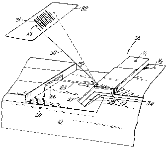
Referring to Figure 2, there is shown a highly simplified
perspective view of a semiconductor structure according to a first
embodiment of the present invention in which the basic elements of
a bar code reader may be implemented.
The substrate 10 includes a first portion including a multiple
layer structure 20, i.e., a semiconductor laser diode, which when
energized, generates a laser beam 25 which is emitted from an edge
26 of the light structure 20. Although the use of reference
numeral 20 in Fig. 2 suggests the use of the structure 20 of Fig.
la, the use of structure 40 of Fig. lb or yet other structures may
be used as well.
The structure 20 generates a laser beam which is propagated
through free space to a reflective structure 33 implemented on the
substrate 10. The beam 25 is more particularly directed to a
reflective surface 27 which is moved or reciprocated by means to
be explained subsequently. The movement of the surface 27 causes
the laser beam 25 to be deflected, so as to produce a scan line or
17
04/24/90 (D-D#044.REV2)
Docket No. 044
other pattern across a symbol 31 disposed on the surface 32 of a
target in the path of the reflected beam.
In the preferred embodiment, the reflective surface 27 is a
layer applied to the top of a piezoelectric composite, 28, 29
disposed on the substrate 10. The composite consists of two layers
of a piezoelectric material responsive to an enabling electrical
signal. A soft, pliable layer 34 of interface material, such as
a glass composition, is applied to the surface of the substrate 10.
The layer 28 which is the first layer of piezoelectric is applied
to the layer 34 and the second layer of piezoelectric material 29
is applied on top of the layer 28. The layer 34 permits the layers
28 and 29 to move with respect to one another without transmitting
such stresses to the substrate 10. An electrode V1 is connected
to the layer of piezoelectric 29, and electrode V2 is connected to
the layer of piezoelectric material 28. The layers of piezo-
electric material preferably comprise lead zirconate and lead
titanate, also known as PZT.
When an electric current is applied to the electrodes V1 and
V2 the relative position of the layers 28 and 29 move as is known
in the art, which results in a deflection of the reflective surface
18
~ , ~ :-s .~ ~ ~~
04/24/90 (D-D#044.REV2)
Docket No. 044
29. The electric signals applied to the electrodes V1 and V2
therefore function to repetitively and cyclically changing the
position of the reflective element in the path of the laser beam
25 so as to transform the laser beam 25 into a scanning beam 30 for
repetitively scanning the target 32 for reflection therefrom.
The plane of the layer of the reflective surface is disposed
at an acute angle with respect to the laser beam 25 so that the
beam is directed along an optical path toward indicia 31 located
in~the vicinity of a reference plane 32 lying in the optical path
so as to scan spatially adjacent portions of the reference plane
32 along a relatively elongated scanning line 33.
Referring next to Fig. 3 there is shown a highly simplified
perspective view of a semiconductor structure according to a second
embodiment of the present invention. As in Fig. 2, the structure
consists of a substrate 10 including a first portion consisting of
a multiple layer structure 20, i.e., a semiconductor laser diode,
which when energized, generates a laser beam 25.
The beam 25 is directed to a polarity of reflective surfaces
50a, 50b, 50c, 50d, 50e, etc. , which are implemented on the surface
19
04/24/90 (D~D#044.REV2)
DOCket NO. 044
of the substrate 10. More particularly the reflective elements
50a, 50b, etc., are micromirrors which are attached to support
posts 51a, 51b, etc., on the surface of the substrate 10. The
mirror surfaces 50a, 50b, etc., lie over and spaced apart from a
pattern of control electrodes 52, 53, 54, etc., which are
repetively and cyclically energized so as to cause the mirror
surfaces 50a, 50b, etc., to rotate on the pivot posts 501a, 51b,
etc. The rotation of the mirror surfaces through a relatively
small angle results in the laser beam striking the surface of the
mirror surfaces being deflected as is shown in the reflected beams
25a and 25b. The movement of the laser beam 25 produces a scan
line of other pattern across a symbol 31 disposed on a target in
the path of the reflected beam.
The arrangement according to the present invention may be
packaged in an integrated circuit package with a window for the
emitted laser beam and implemented on a printed circuit (PC) board
with other electronic components. Such PC board may be packaged
in a hand-held scanner, a desktop workstation or stationery
scanner. In a preferred embodiment, the arrangement would be
implemented in a housing that includes an exit port through which
an outgoing laser light beam 30 is directed to impinge on, and to
CA 02021519 2000-10-16
04/24/90 (D-D~044.REV2)
Doek~t No. 044
be scanned across, symbols 31 located on a target 32 situated
exterior of the housing.
Before describing the third embodiment of the present
invention, it is worthwhile to illustrate the packaging or
implementation of the arrangement according to the present
invention.
As an example of such an embodiment, we described the
implementation of the present invention in a hand-held, laser-
scanning, bar code reader unit such as illustrated in Figure 4.
This hand-held device of Figure 4 is generally of the style
disclosed in U.S. Patent 4,760,248, issued to Swartz et al,
assigned to Symbol Technologies, Inc., and also similar to the
configuration of a bar code reader commercially available as part
number LS 8100 or LS 2000 from Symbol Technologies, Inc.
Alternatively, or in addition, features of U.S. Patent 4,387,297
issued to Swartz et al, or U.S. Patent 4,409,470 issued to Shepard
et al, both such patents assigned to Symbol Technologies, Inc.,
may be employed in constructing the bar code reader unit of Figure
4.
21
04/24/90 (D-D~044.REV2)
Docket No. 044
The operation of such a unit may be described as follows: A
outgoing light beam 151 is generated in the reader 100, usually by
a laser diode or the like, and directed to impinge upon a bar code
symbol spaced at a distance from the front of the reader unit. The
outgoing beam 151 is scanned in a fixed linear pattern, and the
user positions the hand-held unit so this scan pattern traverses
the symbol to be read. Reflected light 152 from the symbol is
detected by a light-responsive device 146 in the reader unit,
producing serial electrical signals to be processed for identifying
the bar code. The reader unit 100 is a gun shaped device, having
a pistol-grip type of handle 153 and movable trigger 154 is
employed to allow the user to activate the light beam 151 and
detector circuitry when pointed at the symbol to be read, thereby
saving battery life if the unit is self-powered. A light-weight
plastic housing 155 contains the laser light source, the
detector 146, the optics and signal processing circuitry, and the
CPU 140 as well as a battery 162. A light-transmissive window 156
in the front end of the housing 155 allows the outgoing light beam
151 to exit and the incoming reflected light 152 to enter. The
reader 100 is designed to be aimed at a bar code symbol by the user
from a position where the reader 100 is spaced from the symbol,
i.e., not touching the symbol or moving across the symbol.
22
04/24/90 (D-D~044.REV2)
Docket No. 044
Typically, this type of hand-held bar code reader is specified to
operate in the range of perhaps several inches.
~s seen in Figure 4, a suitable lens 157 (or multiple lens
system) is used to collimate and focus the scanned beam into the
bar code symbol at an appropriate reference plane, and this same
lens 157 may be used to focus the reflected light 152. A scanning
light source 158 such as a semiconductor device according to the
present invention is positioned to introduce a light beam into the
axis of the lens 157 by appropriate beam-shaping structure needed,
when the trigger 154 is pulled. If the light produced by the
source 158 is not visible, an aiming light may be included in the
optical system to introduce the beam into the light path coaxially
with the lens 157. The aiming light, if needed, produces a
visible-light spot which is scanned just like the laser beam; the
user may employ this visible light to aim the reader unit at the
symbol before pulling the trigger 154 to activate the scanning.
Turning to Fig. 5, there is shown another embodiment of the
present invention in which an entire scanner is implemented on a
silicon substrate. A silicon substrate 200 is provided which
includes a layer 201 composed of GaAs on a portion of the surface
23
04/24/90 (D-D#044.REV2)
Docket No. 044
thereof. On top of the layer 201 is a sequence of layers 202 which
form a semiconductor laser such as shown in Fig. la and lb. The
output laser beam from the semiconductor laser is directed to a
piezoelectric scan element 203 which is also implemented on the
surface of the silicon substrate 200 in accordance with the present
invention. The scan element 203 may be similar to that of the
composite 28, 29 described in Figure 2.
A number of additional elements of the scanner may also be
implemented on the same silicon substrate 200 as is shown in the
Figure. For example, a monitoring photodiode 204 may be
implemented on the silicon substrate to measure the output of the
semiconductor laser 202. An integrated circuit microcontroller
205 may also be implemented on the same surface of the silicon
substrate 200, along with a decoder 206, digitizer 207,
preamplifier 208, photodiode 209, laser diode driver 210, and
piezoelectric scan element driver 211. All such units may be
connected by means of bus electrodes 212 implemented on the surface
of the chip. Contact pads 213 as is known in the art may be
imohemented on the periphery of the substrate 200 for connection
to external wires and for packaging the integrated circuit into a
package.
24
04/24/90 (D-D#044.REV2)
Docket No. 044
Although the present invention has been described with respect
scanners for reading linear or single line bar codes, it is not
limited to such embodiments, but may also be applicable to more
complex scanning patterns and to stacked or two dimensional bar
codes such as Code 49 and similar symbologies. It is conceivable
that the method of the present invention may also find application
for use with various machine vision or optical character
recognition applications in which information is derived from other
types of indicia such as characters or from the surface
characteristics of the article being scanned.
In all of the various embodiments, the elements of the scanner
may be assembled into a very compact IC package or module. Such
a package or module can interchangeably be used as the laser
scanning element for a variety of different types of data
acquisition systems. For example, the module may be alternately
plugged in and used in a hand-held scanner, a table top scanner
attached to a flexible arm or mounting extending over the surface
of the table or attached to the underside of the table top, or
mounted as a subcomponent or subassembly of a more sophisticated
data acquisition system.
2~~~~
04/24/90 (D-D#044.REV2)
Docket No. 044
The scanning module described above may also be implemented
within a self-contained data acquisition system including one or
more such components as keyboard, display, data storage,
application software, and data bases. Such a system may also
include a communications interface to permit the data acquisition
system to communicate with other components of a local area network
or with the telephone exchange network, either~through a modem or
an ISDN interface, or by low power radio broadcast from the
portable terminal to a stationary receiver.
It will be understood that each of the features described
above, or two or more together, may find a useful application in
other types of scanners and bar code readers differing from the
types described above.
While the invention has been illustrated and described as
embodied in a scanning system implemented on a semiconductor and/or
electro-optical substrate, it is not intended to be limited to the
details shown, since various modifications and structural changes
may be made without departing in any way from the spirit of the
present invention.
26
i
~a2~.~1~
04/24/90 (D-D#044.REV2)
Docket No. 044
.,
Without further analysis, the foregoing will so fully reveal
the gist of the present invention that others can readily adapt it
1
for various applications without omitting features that, from the
standpoint of prior art. fairly constitute essential
characteristics of the generic: of specific aspects of this
invention and, therefore, such adaptions should and are intended
to be comprehended within the meaning and range of equivalence of
the following claims: