Note: Descriptions are shown in the official language in which they were submitted.
2021572
OPTICAL CONTROL DEVICE
FIELD OF THE INVENTION
This invention relates to an optical control
device, and more particularly to, an optical control
device having optical waveguides including a
directional coupler provided on a substrate.
BACKGROUND OF THE INVENTION
The practical use of optical communication
systems has been promoted these days. In this
situation, highly advanced optical communication
systems having, for instance, large capacity, multi-
functions, etc. have been sought. In this tendency,
the generation of light signals at a high speed, and
the highly developed change-over and switching of light
signals have been required to be proposed for a
practical use.
In a conventional optical communication system,
light signals are obtained by direct-modulating current
injected into a semiconductor laser or a light emitting
diode. However, this direct modulation is difficult to
be realized at a speed higher than approximately 10 GHz
due to the effect of relaxation oscillation, and to be
applied to a coherent light transmission system due to
the occurrence of wavelength fluctuation. For the
purpose of overcoming these disadvantages, an external
2021572r
modulator has been used in an optical communication
system. Especially, an optical modulator of a
waveguide type having waveguides including a
directional coupler provided on a substrate is
advantageous in that it is of a compact, a high
efficiency, and a high speed.
On the other hand, an optical switch has been
used to change-over light transmission paths and to
carry out the switching of light signals in a network
system. A conventional optical switch is of a
structure having a prism, a mirror, an optical fiber,
etc. which are adapted to move mechanically. For this
structure, the conventional optical switch is of a low
speed, a low reliability, a large size, etc. so that it
is difficult to be applied to an optical circuit of a
matrix pattern. An optical switch which has been
developed to overcome these disadvantages is also of a
type having optical waveguides including a directional
coupler to realize high speed operation, the
integration of devices, high reliable operation, etc.
Especially, an optical switch utilizing a ferroelectric
material such as lithium niobate (LiNbO3) crystal, etc.
is advantageous in that light absorption is low to
provide a low loss, and electro-optic effect is high to
provide a high efficiency. As such an optical control
device, a directional coupler type optical
modulator/switch, a total reflection type optical
2021~5~
switch, Mach-Zehnder type optical modulator, etc. have
been conventionally reported. When this waveguide type
optical control device is applied to a practically
operated optical communication system, it is
indispensable to provide the reproducibility of
operative characteristics deeply connected to a high
yield of devices along with basic performances such as
low loss, high speed, etc.
On type of a conventional optical control device
has first and second optical waveguides provided on a
substrate of lithium niobate. The optical waveguides
are partly narrowered in parallel interval to provide a
directional coupler on the substrate. The directional
coupler is covered with a buffer layer, on which first
and second control electrodes are provided
correspondingly to the first and second optical
waveguides composing the directional coupler. Both
ends of the first and second optical waveguides provide
first and second light signal input terminals,and first
and second light signal output terminals.
In operation, a light signal supplied to the
first light signal input terminal is propagated through
the first optical waveguide to be supplied to the
directional coupler. When no voltage is applied across
the first and second control electrodes, the light
signal is completely coupled in the directional coupler
to be transferred from the first optical waveguide to
2021~72
the second optical waveguide. Then, the light signal
is propagated through the second optical waveguide to
be supplied from the second light signal output
terminal to a following stage. On the other hand, when
a predetermined voltage is applied across the first and
second control electrodes, the coupling between the
first and second optical waveguides becomes lowered in
the directional coupler. The details of the
conventional optical control device will be explained
in more detail later.
However, the conventional optical control device
has a disadvantage in that the characteristics of the
optical waveguides changes to change a coupling state
of the directional coupler, because the optical
waveguides are affected in the vicinity of the control
electrodes by the fluctuation of a refractive index
which occurs in the substrate of the ferroelectric
crystal in accordance with the piezoelectricity and the
optical elastic effect by distortion locally
accumulated in the vicinity of the control electrodes.
In fabricating the conventional optical control device,
a control electrode film is grown on the buffer layer,
and the control electrode film is etched to provide the
control electrodes by use of a mask having a
predetermined pattern. The control electrodes provides
elastic discontinuity on the substrate, so that the
local distortion occurs in the vicinity of the control
20~ 1 57~
71885-13
electrodes on the substrate.
SUMMARY OF THE INVENTION
Accordingly, it is an object of the invention to provide
an optical control device in which distortion occurring in the
provision of control electrodes is uniformly dispersed.
It is another object of the invention to provide an
optical control device in which a coupling state does not change
in a directional coupler~
It is a further object of the invention to provide an
optical control device having stable characteristics which is
fabricated with a high yield.
According to this invention, an optical control device,
comprising: optical waveguicles provided on a substrate having an
electrooptic effect, said optical waveguides having a
predetermined thickness extending from a surface of said substrate
to predetermined depth thereof; a coupling portion provided on
said substrate by narrowing an interval of said optical
waveguides; a buffer layer provided on said substrate to cover
said optical waveguicles including said coupling portion; control
electrodes for applying a predetermined voltage across said
optical waveguides at said coupling portion, said control
electrodes being provided on said buffer layer; and protrusion and
concave means for dispersing distortion locally accumulated in the
vicinity of said control electrodes to the whole area of said
substrate, said protrusion and concave means being formed on one
of surfaces of said substrate and said buffer layer.
BRIEF DESCRIPTION OF THE DRAWINGS
This invention will be explained in more detail in
J ~
202 1 572
- 6 71885-13
conjunction with appended drawings, wherein:
Figure lA is a plan view showing a conventional optical
control device,
Figure lB is a cross sectional view along a line B-B in
Figure lA,
Figure 2A is a plan view showing an optical control
device in a first preferred embodiment according to the invention,
Figure 2B is a cross sectional view along a line B-B in
Figure 2A,
Figure 3 is a graph showing the change of branching
ratios before and after the formation of control electrodes in the
first preferred embodiment,
Figure 4A is a plan view showing an optical control
device in a second preferred embodiment according to the
invention,
Figure 4B is a cross sectional view along a line B-B in
Figure 4A,
Figure 5 is a graph showing the change of
2a2~57~
branching ratios before and after the formation of
control electrodes in the second preferred embodiment,
Fig. 6A, 7A, and 8A are plan views showing
optical control devices in third to fifth preferred
embodiments according to the invention, respectively,
and
Fig. 6B, 7B, and 8B are cross sectional views
along lines B-B in Figs. 6A, 7A and 8A, respectively.
DESCRIPTION OF THE PREFERRED EMBODIMENTS
Before explaining an optical control device in
the first preferred embodiment according to the
invention, the aforementioned conventional optical
control device will be explained in Figs.1A and1B.
The optical control device comprises optical
waveguides 2 and 3 provided on a substrate1 of lithium
niobate crystal which is cut vertically to Z-axis, and
a directional coupler 4 provided on the substrate 1 by
the optical waveguides 2 and 3 having a narrowed
parallel interval X. The optical waveguides 2 and 3
are formed on the substrate 1 of lithium niobate
crystal by diffusing Ti into portions of the substrate
1 corresponding to the optical waveguide pattern, so
that the Ti-diffused portions become larger in
refractive index than the substrate 1. The directional
coupler 4 is defined to have the narrowed parallel
interval X of several ~m. The optical control device
2021~72
further comprises a buffer layer 6 provided on the
substrate 1 to cover the optical waveguides 2 and 3,
and control electrodes 5 provided on the buffer layer
6. The buffer layer 6 avoids light propagating through
the optical waveguides 2 and 3 to be absorbed by the
control electrodes 5.
In operation, an input light 7is supplied to an
input terminal of the optical waveguide 2 to be
propagated through the optical waveguide 2. When the
propagated light reaches the directional coupler 4, it
is gradually transferred in the directional coupler 4
to the optical waveguide 3 in a state that no voltage
is applied across the control electrodes 5, so that the
light is completely transferred at output terminals of
the directional coupler 4. As a result, an output
light 8 is obtained at an output terminal of the
optical waveguide 3. On the other hand, when a
predetermined voltage is applied across the control
electrodes 5, a refractive index of the optical
waveguides 2 and 3 changes below the control electrodes
5, so that phase mismatch occurs between waveguided
modes of lights propagating through the optical
waveguides 2 and 3. As a result, a coupling state
changes between the optical waveguides 2 and 3 of the
directional coupler 4. Consequently, an output light 9
is obtained at an output terminal of the optical
waveguide 2.
2~2i~ S~
In fabricating the optical control device, a
control electrode film is grown on the buffer layer 6.
Then, the film is etched except for portions of the
control electrodes 5 by photolithography. As a result,
the above described control electrodes 5 are obtained
on the buffer layer 6.
In this fabricating process, it is known that
distortion occurs in the substrate 1 due to the
difference of thermal expansion coefficients of the
substrate 1, the buffer layer 6, and the control
electrodes 5, and the difference of elastic
coefficients such as poisson ratios, etc. thereof, when
films of the buffer layer 6 and the control electrodes
5 are grown, respectively. In this state, generally,
the distortion which has occurred at the grown times of
the films is distributed into the entire area of the
substrate crystal, so that the difference of refractive
indexes does not change between the optical waveguides
2 and 3 and the substrate1, even if absolute values of
the refractive indexes change before and after the
growing of the films. Accordingly, optical waveguide
characteristics which have been obtained at the grown
time of the optical waveguides 2 and 3 is maintained,
so that no change occurs in a coupling state of the
directional coupler 4.
However, distortion which fluctuates at a time
of forming the control electrodes 5 is locally
2~2~ 2
1 0
accumulated in the vicinity of the control electrodes
5, because the control electrodes 5 which are formed by
etching the control electrode film provide elastic
discontinuity on the substrate. As a result of this
distortion, the change of a refractive index occurs in
the ferroelectric crystal substrate 1 in accordance
with piezoelectricity, optical elastic effect, etc.
Consequently, the optical waveguides 2 and 3 are
affected in the vicinity of the control electrodes 5 by
the fluctuation of the refractive index, thereby
changing the optical waveguide characteristics. As a
result, the coupling state of the directional coupler 4
changes to result in the decrease of reproducibility in
providing a coupling state of the directional coupler 4
as designed. The change amount of the coupling state
changes in each batch of the grown films for the buffer
layer 6 and the control electrodes 5. These are
the aforementioned disadvantages of the conventional
optical control device.
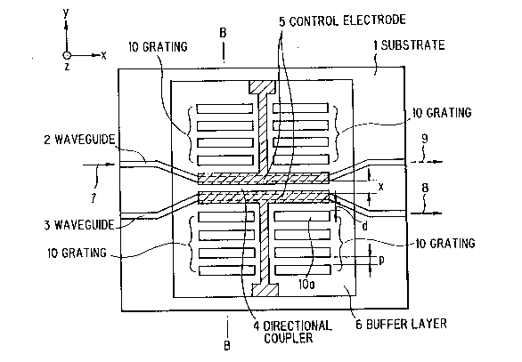
Figs. 2A and 2B show an optical control device
in the first preferred embodiment according to the
invention, wherein like parts are indicated by like
reference numerals as used in Figs. 1A and 1B. The
optical control device comprises optical waveguides 2
and 3 provided on a substrate 1 of lithium niobate
(LiNbO3) crystal which is cut vertically to Z-axis, and
a directional coupler 4 provided on the substrate 1 by
2 02~ 5 ~ ~
1 1
the optical waveguides 2 and 3 having a narrowed
parallel interval X of approximately several ~m. The
optical waveguides 2 and 3 are formed on the substrate
1 of lithium niobate crystal by diffusing Ti into
portions of the substrate 1 corresponding to the
optical waveguide pattern, so that the Ti-diffused
portions are larger in refractive index than the
substrate 1. The diffusion of Ti is carried out at a
temperature of approximately 900 to 1100C for several
hours to provide the optical waveguides having a depth
of approximately 3 to 10 ~m. In addition, the optical
control device comprises a buffer layer 6 of SiO2 which
is optically transparent and lower in refractive index
than the substrate 1, and control electrodes 5 having
two metal layers of Cr and Au provided on the buffer
layer 6. In this structure, the absorption of light is
avoided from the optical waveguides 2 and 3 to the
control electrodes 5 by the buffer layer 6. The
optical control device further comprises four groups of
gratings 20 in the vicinity of and parallel to the
control electrodes 5 provided on the buffer layer 6.
Each of the gratings 10 is of the same material as the
control electrodes 5, and includes plural grating
elements 1Oa having the same length and width as each
other and arranged to be parallel with a pitch of 40 to
60~m. A grating element 1Oa which is positioned in
the nearest vicinity of a corresponding one of the
2 0 2~ Z
control electrodes 5 has a distance d from the
corresponding control electrode 5.
In fabricating the optical control device, the
gratings 10 are formed simultaneously with or prior to
the formation of the control electrodes 5 by etching a
control electrode film grown on the buffer layer 6. In
other words, the control electrode film is removed by a
pattern excepting the control electrodes 5 and the
gratings 10. In this stage, if the control electrodes
5 are formed prior to the formation of the gratings 10,
distortion which has occurred in elastic discontinuity
region due to the formation of the control electrodes 5
remains even after the formation of the gratings 10.
The gratings 10 may have a pitch which is increased, as
the distance is increased from the corresponding
control electrode 5, instead of the aforementioned
constant pitch, and the width of the grating elements
1Oa is not always required to be constant, and
parallel, but slant to some extent. Even more, the
gratings 10 are preferable to be connected to the
ground, so that the accumulation of charge is avoided
in the buffer layer 6. In the modification of the
stripe gratings 10, square shaped protrusions each
having a side of approximately 40 ~m and of the same
material as the control electrodes 5 may be provided on
the buffer layer 6 to be arranged vertically and
horizontally to the control electrodes 5 in a
2021~7~
13
periodical pattern having the same pitch. In short,
when small protrusions are formed around the control
electrodes 5 prior to or simultaneously with the
formation of the control electrodes 5, distortion which
has occurred in the substrate 1 is uniformly dispersed
into elastic discontinuity points.
Fig. 3 shows the difference in coupling states
of the directional couplers 4 between the conventional
optical control device and the optical control device
in the first preferred embodiment. The coupling state
is determined in accordance with a branching ratio
which is defined by P1/Pi, where Pi is an input light
power supplied to an input terminal 4a of the
directional coupler 4, and P1 and P2 are output light
powers supplied from output terminals 4b and 4c of the
directional coupler 4 (Pi = P1 + P2), as shown in Fig.
3. In this experiment, light of TE mode is used. The
branching ratio P1/Pi changes before (without) and
after (with) the formation of the control electrodes 5.
In Fig. 3, a line I indicates the change in the
conventional optical control device, and a line II
indicates the change in the optical control device in
the preferred embodiment. As apparent from the
comparison between the lines I and II, the change of
the branching ratio P1/Pi is substantially negligible
in the present invention, so that light of
approximately 100% is transferred from one optical
2021572
14
waveguide to the other optical waveguide, while the
change of the branching ratio P1/Pi is approximately
50%, so that light of approximately 50% is not
transferred from one optical waveguide to the other
optical waveguide to provide light of 50% which is only
propagated through one optical waveguide in the
conventional optical control device.
Figs. 4A and 4B show an optical control device
in the second preferred embodiment according to the
invention, wherein like parts are indicated by like
reference numerals as used in Figs. 2A and 2B. This
optical control device is characterized by the
provision of periodical stripe protrusions 20 which are
parallel to control electrodes 5 on a substrate 1. A
protrusion 20 which is in the nearest vicinity of a
corresponding control electrode 5 in each of the four
group protrusions 20 is positioned to have a distance d
of 5 to 500~m. A ratio of a pitch and a width of the
protrusions 20 is not limited to be a specified value,
but may be an adequate value such as 1. In the second
preferred embodiment, it is important that the
protrusions 20 are formed prior to the formation of
the control electrodes 5.
Fig. 5 shows branching ratios P1/Pi of the
conventional optical control device and the optical
control device in the second preferred embodiment. As
apparent from the comparison between lines I and II
2021~7~
indicating the branching ratios P1/Pi of the
conventional optical control device and the present
invention, respectively, a change of the branching
ratio P1/Pi before and after the formation of control
electrodes 5 is negligible in the invention, while that
of the conventional optical control device ranges 20 to
60%.
The periodical protrusions 20 are formed by the
steps of growing a film for a buffer layer 6 on the
substrate 1, forming a periodical mask pattern
corresponding to the periodical protrusions 20 on the
film by photolithography, and etching the film to
provide the periodical protrusions 20 and the buffer
layer 6 by use of dry etching method such as ion beam,
reactive ion, and reactive ion beam etchings, or wet
etching method utilizing etchant. The periodical
protrusions 20 may be formed by use of focused ion beam
etching method, so that the step of using
photolithography is not necessary. The buffer layer 6
is formed to be lower in refractive index than the
substrate 1 of lithium niobate by SiO2, SiON, MgF2,
Si3N4, Al2O3, etc., and of less light absorption
property.
Figs. 6A and 6B show an optical control device
in the third preferred embodiment according to the
invention, wherein like parts are indicated by like
reference numerals as used in Figs. 4A and 4B. In this
20215~
16
third preferred embodiment, four groups of periodical
net shapedconcaves 40 are provided on a buffer layer 6
and at the surface of the substrate 1 prior to the
formation of control electrodes 5 in place of the
protrusions 20 in the second preferred embodiment. In
the third preferred embodiment, the same result is
obtained in regard to the change of a branching ratio
as in the second preferred embodiment.
Figs. 7A and 7B show an optical control device
in the fourth preferred embodiment according to the
invention, wherein like parts are indicated by like
reference numerals as used in Figs. 4A and 4B. In this
fourth preferred embodiment, four groups of periodical
matrix shaped concaves 50 are provided on a buffer
layer 6 and at the surface of the substrate 1 prior to
the formation of control electrodes 5 in place of the
protrusions 20 in the second preferred embodiment. In
the fourth preferred embodiment, the same result is
obtained in regard to the change of a branching ratio
as in the second preferred embodiment.
Figs. 8A and 8B show an optical control device
in the fifth preferred embodiment according to the
invention, wherein like parts are indicated by like
reference numerals as used in Figs. 2A and 2B. In this
fifth preferred embodiment, four groups of periodical
net shaped protrusions 60 of the same material as a
buffer layer 6 are provided on the buffer layer 6 prior
2021~72
to the formation of the control electrodes 5 in place
of the gratings 10 in the first preferred embodiment.
In the fifth preferred embodiment, the same result is
obtained in regard to the change of a branching ratio
as in the second preferred embodiment.
In the fifth preferred embodiment, the net
shaped protrusions 60 may be provided by the same
material as control electrodes 5. In such a case, a
control electrode film is grown on the buffer layer 6,
and a mask pattern correponding to the net shaped
protrusions 60 and the control electrodes 5 is provided
on the control electrode film by lithography. Then,
the control electrode film is etched to be removed by
use of dry etching method such as ion beam etching,
reactive ion etching, reactive ion beam etching, etc.
or chemical wet etching method utilizing etchant. The
control electrodes 5 and the net shaped protrusions 60
may be directly drawn on the buffer layer 6 by use of
focused ion beam etching method. The net shaped
protrusions 60 may be provided on the buffer layer 6 by
a material different from the control electrodes 5. In
such a case, a metal film or an insulating material
film is provided on the buffer layer, before the
control electrodes 5 are provided on the buffer layer
6. The film is etched to be removed, thereby providing
a net shaped protrusions of the metal or the insulating
material by use of the above described etching method.
20215 ~ 2
As fully explained above, periodical stripe, net
shaped, or matrix shaped gratings, concaves or
protrusions are provided on a buffer layer, or a
substrate in the invention. According to an experiment
conducted by the inventors, it is confirmed that the
change of a coupling state of a directional coupler
which occurs by the formation of control electrodes is
suppressed by providing the gratings, concaves, or
protrusions in the vicinity of the control electrodes.
It is generally known that distortion tends to be
accumulated in elastic discontinuity regions of a
substrate. Before providing control electrodes on the
buffer layer, the distortion is uniformly distributed
to keep a balance in the substrate. Then, when the
control electrode is provided on the buffer layer by
etching a control electrode film, the balance of the
distortion is no longer maintained to be shifted to a
second balance state. In this state, the distortion is
converged into the elastic discontinuity regions, if
the regions exist in the substrate. As described
before, only control electrodes exist on the substrate
as elastic discontinuity regions which are produced by
the formation of the control electrodes. When the
distortion is shifted to the second balance state of
distortion, therefore, the distortion is conveyed in
the vicinity of the control electrodes, so that a
coupling state of a directional coupler changes
2021~72
1 9
largely. This is a disadvantage of the conventional
optical control device. On the other hand, a number of
elastic discontinuity regions are formed on the
substrate in the invention. For this reason, the
distortion disperses to the elastic discontinuity
regions thus formed on the substrate to provide a
balance state, when the control electrodes are
provided. In other words, distortion to be accumulated
in the vicinity of the control electrodes is much
decreased as compared to the conventional optical
control device. This suppresses the change of a
refractive index of a ferroelectric crystal in the
vicinity of optical waveguides provided thereon.
Accordingly, optical waveguide characteristics which
are determined at the time of forming the optical
waveguides on the ferroelectric crystal substrate are
maintained to provide no change of a coupling state of
the directional coupler. Thus, an optical control
device according to the invention has predetermined
characteristics as designed, and is stably fabricated
with a high yield.
Although the invention has been described with
respect to specific embodiment for complete and clear
disclosure, the appended claims are not to be thus
limited but are to be construed as embodying all
modification and alternative constructions that may
occur to one skilled in the art which fairly fall
2 ~ 2 1 ~ ~ r2
within the basic teaching herein set forth.