Note: Descriptions are shown in the official language in which they were submitted.
2 ~ 3~l
-1- RD 16,987
SWEPT FREQUENCY EDDY CURRENT SYSTEM FOR
.
MEASURING COATING THICKNESS
Backqround of the Invention
The present invention relates to measuring coat-
ing thickness, and more particularly, to using eddy currentapparatus with a swept frequency oscillator.
When substrate parts are coated with thin layers,
it is important to control the layer thickness. When the
coating has physical properties, e.g., acoustic impedance
or electrical resistivity, which are distinctly different
from the substrate, control of layer thickness is done with
standard techniques, such as ultrasound or fixed frequency
eddy currents. However, in coating some substrate parts,
the substrate and coating materials differ only slightly,
e.g., the coating of zircalloy tubing with zirconium metal.
Thus, the difference in physical properties is slight,
which makes determining coating thickness difficult.
It is therefore an object of the present inven-
tion to determine coating thickness, especially when the
difference in physical properties of the coating and the
substrate are small.
Su~marv of ~he Invention
In brief, this and other objects are achieved by
apparatus in accordance with the invention for measuring
the thickness of a coating on a substrate having a given
substrate material, comprising means for generating
variable freguency eddy currents in the coated substrate,
the coating, and an uncoated sub~trate of the given
ma~erial; and means for comparing conductivity changes of
the coating and the coated subs~rate wi~h the uncoated
substrate with changes in fr~quency.
A method in accordance with the invention for
measuring the thickness of a coating on a substrate having
a given substrate material, comprises generating variable
frequency eddy currents in the coated substrate, the
coating, and an uncoated substrate of the given ma~erial;
and comparing changes in conductivity of the coating and
-2- RD 16,987
the coated substrate with the uncoated substrate with
changes in frequency.
Brief Descr_~tion of the Drawinq
Figure 1 is a blocX diagram of an embodiment of
the invention;
Figure 2 is a cross-sectional view of the dispo-
sition of probe coils used in Figure 1.
Figure 3 is a cross-sectional view of an angle
block used to calibrate the invention;
Figure 4 is a graph of a signal in the embodiment
of Figure 1; and
Figure 5 is a partial block diagram a~other
embodiment of the invention.
Detailed DescriDtion
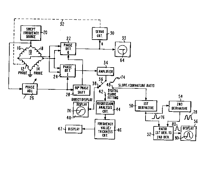
Figure 1 shows a bridge circuity 10 including
probe coils 12 and 14 each having one end grounded. Bridge
10 also comprises inductances 16 and 18 that are
respectively coupled to the remaining ends of probes 12 and
14. While inductances 16 and la can be replaced with
resistors or capacitoxs, it is pre~erable that they be
inductances so that the sensitivity of bridge 10 is
maintained over a wide frequency range. A swept frequency
signal source or oscillator 20 is coupled to the remaining
ends of inductances 16 and 18. Source 20 has a typical
fre~uency sweep of between about 10 K~z to 10 MEz, with a
sweep rate of ~bout 30 Hz, although other frequencies can
be used. Pre~erably, source 20 is a constant current (high
output impedance) source in order to further help maintain
bridge sensitivity over the swept frequency range.
~omparison means, such as phase detectors 22 and
24, each have a pair of inputs respectively coupled to the
junction of coils 12 and 16 and also to the junction of
coils 14 and 18. Source 20 provides a signal to the input
of a phase adjuster 26. The output signal from adjuster 26
is directly applied to an input of detector 24 and also to
the input of a 90 degree phase shift circuit 28; the
output signal from circuit 28 is applied to detector 22.
2~ f~ ~'
~3- RD 16,g87
Thus detector 22 ls the Q (quadrature) channel phase
detector, while detector 24 is the I (in-phase) channel
phase detector.
As know in the art, detectors 22 and 24 can each
comprise a diode bridge with the differential signal from
probes 12 and 14 ~nd from source 20 as input signals. An
output signal from the bridge is applied to a
resistance-capacitance low pass filter. This filter should
have a time constant longer than the period of the low
frequency limit of the frequency sweep, e.g., l/lOKHz, and
shorter than the period of the sweep rate, e~g., 1/30 Hz.
Phase detectors 22 and 24 essentially pass the differential
signal from probes 12 and 14 if it is in phase with that of
the reference oscillator signal applied to the respective
detector and do not pass ~he differential input signal if
it is out of phase therewith.
The output signal from Q channel detector 22 is
applied to a servo circuit 30, which includes a mechanical
manipulator (not shown) for controlling the position of
probe 12 as shown by dotted line 32. The output signal
from Q channel detector 22 is also applied to the vertical
axi-s input of a CRT display 33, which has a horizontal axis
time sweep synchronized with the frequency sweep of source
20.
The output signal from I channel detector 24 is
applied to the input of an amplifier 34, which amplifier
provides an out.put signal to switch 36. When switch 36
engages contact: 38 for a direct display mode, the amplifier
34 output signal is applied to the vertical axis input of a
CRT display 40, which also has a horizontal axis time sweep
synchronized with the frequency sweep of source 20 in order
to display a transition frequency (explained below).
When switch 36 engages contac~ 42, a digital
curve fitting mode is selected. Said amplifier 34 output
signal is applied to a regression analysis circuit 44,
which can comprise a microprocessor progra~med to perform a
least squares fit, maximum likelihood technique, etc., as
known in the art, in order to determine the transition
2 ~
-4- RD 16,987
frequency. A hardwired circuit could also be used. The
transltion frequency output signal from circuit 44 is
applied to a circuit 46 , e.g., a ROM, that has been
calibrated with a table of coating thickness versus
transition frequencies (explained below). The coating
thickness output signal from circuit 46 is applied to a
display 47, which can be either an analog or digital
display of the coating thickness.
When switch 36 engages contact 48, said amplifier
34 output signal is applied to a di~ferentiator 50 to com-
pute the first derivative of said output signal. The
output signal from differentiator 50 is applied to a ratio
circuit 52, which can comprise a microprocessor programmed
to compute a ratio. Hardwired digital and analog circuits
for computing ratios can also be used as is known in the
art. The output signal from differentiator 50 is also
applied to differentiator 54 in order to compute the second
derivative of the amplifier 34 output signal. The output
signal from differentiator 54 is applied to ratio circuit
52. The output signal from ratio circuit 52 is applied to
the vertical axis input of a CRT display 56, which also has
a horizontal axis time sweep synchronized with the
frequency sweep of source 20. It will be seen that
displays 33, 40 and 56 can be the same display with a
switch (not shown) switching the input of the display
between the outputs of circuits 22, 34 or 52 in accordance
with the position of switch 36 or the phase adjust
operation (described below). A dual trace oscilloscope can
also be used as the display.
As shown in Figure 2(a), during the first
operation, called "phase ad]ust", probe 12 is placed near,
and the coil axis preferably perpendicular to, a substrate
58 having a co~ting or cladding 60 of either known or
unknown thickness. Probe 14 is placed near, and the coil
axis perpendicular to, an uncoated reference substrate 62
of the sa~e material as substrate 58, as shown in Figure
2(b). In general, substrates 58 and 62 and coating 60 can
be any conductive material, e.g. metals, conductive
-5- RD 16,987
plastics, composite materials, etc. Bo~h probes 12 and 14
and substrates 58 and 60 are normally motionless. A swept
frequency signal is generated by source 20 that creates
eddy currents in substrates 58 and 62 and coating 60 in
accordance with their respective conductivities at the
instantaneous frequency. Q channel phase detector 22
compares these conductivities by comparing the magnitude
and phase of the voltages the eddy currents generate in
coils 12 and 14, which comparison is displayed on display
33. Phase adjustment circuit 26 is then adjusted in order
to give the most horizontal possible display line 64 on
display 33, i.e., the minimum possible sensitivity of Q
channel detector 22 to differences in conductivity changes.
This approximately corresponds to the maximum sensitivity
of I channel detector 22 to differential conductivity
changes of substrates 58 and coating 60 compared to
substrate 62 and also to the maximum sensitivity of Q
channel detector 22 to changes in the distance between
probe 12 and the substrate 58. Such later changes are
called "lift-off".
The next step is calibration, and, as shown in
Figure 3, probe 12 is disposed proximate a substrate 66
having an angle lapped wedge-shaped coating 68. The
thickness of coating 68 varies in a known manner with
distance alo~g substrate 66. Instead of being
wedge-shaped, coating 68 can be staircase (step) shaped
with the steps of known thickness. Probe 14 is still
disposed as shown in Figure 2(b). Source 20 is activated
and its frequency is swept. When probe 12 is near a thin
portion of coating 68 and the frequency is low, eddy
currents penetra~e both coating 68 and substra~e 66. Thus
the signals from probes 12 and 14 are nearly equal and
bridge 10 is nearly in balance since probes 12 and 14 are
essentially respectively measuring the conductivity of
substrates 66 and 62, which are equal. As the frequency is
raised, the balance initially remains constant, but
eventually the skin effect causes less and less of the eddy
currents to penetrate substrate 66 and bridge imbalance
-6- RD 16,987
increases, see curve 70 in Figure 4. Finally, the
imbalance levels off since the conductivity primarily of
coating 68 is being measured. Half way between these two
level portions of curve 70 is a transition frequency f2,
which occurs where the thickness of coating 68 is about
equal to the skin depth. Since the coating thickness is
known, a calibration point of frequency versus thickness is
obtained and stored in circuit 46 and the horizontal axes
of displays 40 and 56 are calibrated. Probe 12 is then
moved to be disposed near a thicker portion of coating 68
and ~he process repeated as shown by curve 72. This time a
new transition frequency fl, is obtained, wherein f2 is
greater than fl. The new calibration point is stored in
circuit 46 and the horizontal axes of displays 40 and 56
are calibrated. This process is repeated several times
until a sufficient number of calibration points are
obtained. Obviously, a thick coating can be first used for
calibration and then thinner coatings.
The next step is to use the apparatus of the
invention to measure the thickness of an unknown coating by
disposing probe 12 near a substrate 58 having a coating 60
of unknown thickness, as shown in Figure 2(a). Probe 12 is
~lowly scanned in a one or two dimensional pattern over
substrate 58. Alternatively, substrate 58 can be moved
while probe 12 is stationary, or some combination of both
motions can be used especially for a two dimensional scan
wherein one of ~aid motions can be in one direction and the
other motion can be perpendicular ~o said one direction.
By "slowly" is meant that this mecham cal scan is slow
compared to the sweep rate of source 2Q. If desired,
during this scan the output signal from Q-channel detector
22 can be used to control servo circuit 30 which in turn
keeps the distance between probe 12 and substrate 58
substantially a constant, i.e., minimizes lift-off, for
more accurate thickness measurements. Probe 14 is still
disposed as shown in Figure 2(b).
Amplifier 34 provides a signal such as shown by
numeral 74 in figure 1. If the direct display mode is
_7- RD 16,987
chosen by switch 36, signal 74 wlll be displayed by display
40. If the digital curve fitting mode is chosen,
regression analysis circuit 44 determines the transition
freguency of best fit to the signal 74. Then a signal
representing this frequency is applied to circuit 46 and a
thickness corresponding to this frequency and read out and
displayed by display 47.
If the slope-curvature ratio mode is selected,
then bridge imbalance is not directly used but the first
derivative of signal 74 is calculated by circuit 50 as
shown by signal 76. Then the second derivative of signal
74 is calculated by circuit 54 as shown by signal 78. The
ratio of signal 76 to that of signal 78 is then calculated
by circuit 52. At high and low frequencies the first
derivative is small. At the transition frequency the
derivative is large and the second derivative goes to zero.
The ratio is a maximum at the inflection point of the
bridge unbalance vs frequency curve as shown by signal 80.
Thus this method is a very sensitive measure of transition
freguency. Sig~al 80 is then displayed by display 56.
If desired, and if a two dimensional scan is
used, the output signal from amplifier 34 can be used to
make a spatial image on a display (not shown) in either
gray scale or color.
It will be appreciated that the present in~ention
provides a sensitive apparatus and method for measuring the
thic~ness of a coating on a substrate even when the
physical properties of the coating and substrate are small.
It will be further appreciated that many other embodiments
are possible within the spirit and scope of the invention.
For example, as shown in Figure 5, instead of being a part
of a bridge circuit 10, probes 12 and 14 can be coupled to
respective inputs of a difference amplifier 82 co~paring
means. One input of each of the detectors 22 and 24 is
coupled to the output of amplifier 82, while the remaining
input of each of detectors 22 and 24 is grounded. The rest
of the circuit is identical to that shown in Figure 1.