Note: Descriptions are shown in the official language in which they were submitted.
20217~ -
A BI-PHASE CODE GENERATION AND AMPLIFICATION CIRCUIT
FOR MICROWAVE AND MILLINETER-WAVE FREQUENCIBS
., ~ ~ `, ., ! . .
BACR~ROUND OF THE INVENTION
;'.' ' '''" ' '
''.'. ,' .":- '-'
Field of the Invention: `
~`
The present invention relates to electronic circuits - -
used for bi-phase code generation. More specifically,
the present invention relates to injection locked voltage
controlled oscillator (VCO) circuits used for bi-phase ~ ~ `
code generation with signal amplification.
While the present invention is described herein with `
reference to an illustrative embodiment for a particular ~-
application, it is understood that the invention is not
limited thereto. Those having ordinary skill in the art
15 and access to the teachings provided herein will recog- ~ ~
nize additional modifications, applications and embodi- ~ -
ments within the scope of the present invention.
pescription of the Related Art:
Bi-phase code generation is a method for encoding
digital information onto a constant frequency signal by~
phase modulating the signal between two distinct phase
states. One phase state of the signal is used to
25 represent a digital '1', while the other phase state is -~
;used to represent a digital '0'. Using this method,
digital information can be transmitted by a signal -`~
operating at a single frequency.
~. ~
- ::
'
:~: -,. ~-: .
' ' - .
' ''" '.
-- 202~
,
Bi-phase coded microwave and millimeter-wave signals
are widely used in high resolution radar and spread
spectrum applications. Conventional systems of these
types which require bi-phase coding typically encode
digital data onto an intermediate frequency (I.F.) signal
using a PIN diode modulator. The resulting bi-phase
coded I.F. signal must then be amplified. Upconversion to
the final output frequency is performed with a mixer
circuit using a second I.F. signal with a frequency
located in the range of the final output frequency. The
upconverted bi-phase coded signal output by the mixer
circuit must then be filtered by a suitable bandpass
filter to remove spurious frequency components generated
by the mixing process. The resulting signal is again
amplified to achieve the final output signal level.
This conventional method of bi-phase code generation
for microwave and millimeter-wave signals has three
shortcomings. One problem is the large amount of
circuitry required to implement the modulation, mixing,
filtering and amplification stages used in this type of
design. A second problem is due to a reduction in the
signal to noise ratio of the final output signal caused
by conversion losses and electrical noise added by each
of the various stages used to process the signal. And
third, since the modulation process attenuates the
signal, many amplifiers are required to achieve an
appropriate signal level.
Although not specifically designed for bi-phase code
generation, a simplified system for providing phase
modulated output from a synchronized oscillator chain has
been described by Helmut Barth, "A 94 GHz Synchronized
Oscillator Chain for Fast, Continuous 360 Degree Phase
Modulation," IEEE MTT-S Digest, 1987. This system uses
two second harmonic mode oscillators having output ports
for their fundamental and second harmonic waves. The
' .- : '
.: -. : - .,: . . . .
2 0 2 1 7 4~
fundamental output ports of the two oscillators are
connected by a waveguide which allows one of the
oscillators (a varactor tuned slave oscillator) to be
locked at its fundamental frequency by a fixed, tuned
master oscillator. The phase difference between the
second harmonic outputs of each of the oscillators can
then be controlled by changing the tuning voltage applied
to the varactor of the slave oscillator.
Although this system represents an improvement over
prior phase modulation systems, it also suffers from
three significant limitations. The first limitation is
that the system only provides phase modulated output
signals of the second harmonic frequency of the
oscillator chain. The second limitation is that the
power levels of the second harmonic signals output by the
system are substantially less than the power levels of
the fundamental frequency signals produced by the
oscillator chain, resulting in a net loss of output
signal power. The third limitation is that the
construction and tuning of the waveguide connecting the
two oscillators is critical to the operation of the
system, making fabrication of the system a difficult
task.
Accordingly, there is a need in the art for a simple
bi-phase code generation system fabricated from readily
available components which can directly phase modulate
and amplify microwave or millimeter wave signals without
the use of intermediate frequencies.
-
SUMMARY OF THE INVENTION
The need in the art is addressed by the present
invention which provides a bi-phase code generation
system with gain for microwave and millimeter-wave
signals.
~,
: : ~, .
.
~::
`' :~
2 0 2 1 ~ ~ 9
4 ~
~: ~
The invention includes a voltage controlled
oscillator (VCO), a tuning voltage source, and injection
locking circuitry for injection locking the voltage
controlled oscillator to the frequency of an injected -
signal. In a specific embodiment, the injection locking
circuitry includes a three port circulator, and a locking
frequency source. A locking frequency reference signal
is applied to the first port of the three port circulator ;~
and the output of the VCO is connected to the second
port of the circulator. The power level of the reference
signal is significantly less than the power of the signal ~ ~ ;
generated by the VCO. Since the circulator allows
propagation of radio frequency energy in one direction
only, this arrangement causes the signal output by the
VCO to be locked to the frequency of the reference
signal. Thus, the resulting signal output from port 3 of
the circulator possesses both the frequency stability of
the reference signal and the amplified power level of the ~ ;~
VCO signal. As the frequency of the signal output by the ~;
VCo is locked to the frequency of the reference signal, a
change in the tuning voltage applied to the VCO produces
a change in the phase of the output signal. This allows
the final output signal of the injection locked VCO to be ~-~
phase modulated in accordance with the tuning voltage
applied to the VCO. Therefore, instead of a loss in the
signal power of the reference frequency, as encountered
in conventional systems, the final phase modulated signal -
output from port 3 of the circulator exhibits a net gain
in power provided by the VCO. ~ ~
~ -;
BRIEF DESCRIPTION OF THE DRAWINGS
Figure l(a) is a block diagram of the present
invention.
35 Figure l(b) is a graph illustrating the
. . ` :
2 ~ 2 1 7 9! ~
: 5
, ~:
relationship between the locking signal and the signal
output by the injection locked voltage controlled
oscillator (VCO) with an applied tuning voltage VT1. :~
Figure l(c) is a graph illustrating the relationship
between the locking signal and the signal output by the
injection locked VCO with an applied tuning voltage VT2.
Figure 2 is a simplified block diagram of a
conventional (non-injection locked) VCO. : - :.:
Figure 3 is a graph illustrating the frequency .
10 response of an injection locked VCO operated with two : .~:~
different tuning voltages.
Figure 4 is a block diagram of an alternative ..
embodiment of the present invention using an amplifier
with an electrically tunable impedance matching network
15 in place of a VCO. ~ ~;
,
DESCRIP~ION OF THE INVENTION
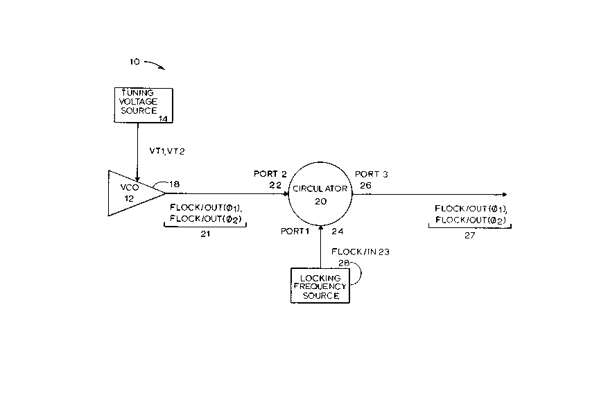
Figure l(a) shows a block diagram of the bi-phase .
20 code generation system of the present invention. The ~::.:
bi-phase code generation system 10 includes a voltage :~
controlled oscillator (VCO) 12, a tuning voltage source
14, a three-port circulator 20, and a locking frequency
reference source 28. :
The output of the VCO 18 is connected to a second -~
input port 22 of the three-port circulator 20. The three ;~
port circulator is a standard type of ferromagnetic
device which is readily available from companies such as
Microwave Associates (LOCATION). The locking frequency : ~ .
reference source 28 injects a locking frequency signal (F
LOCK/IN 23) into a first input port 24 of the three-port ~-.. :-
circulator 20. The low power locking frequency signal (F
LOCK/IN 23) injected into the second input port 24 of the
circulator 20 modulates the active impedance of the VCO's -~
active microwave device in.a manner which effectively
;,.'-,'','.,:
' ' `"~``" '
' ' . ' ' '
2021 7~
locks the output frequency of the VCO (FLOCK/OUT 21) to
the locking signal frequency (FlOCK/IN 23).
As shown in Figure l(b), this technique allows the
VCo's output signal FLOCK/OUT(~1) 30 to be locked to the
frequency of the locking reference signal F lock/In 32.
The phase difference between the two signals is a
function of the tuning voltage applied to the VCO, and
will be discussed in more detail below. Since the
injection locking process allows the lower power locking
reference signal FLOCK/IN 32 to control the higher power
output signal of the VCO (FLOCK/OUT 30), this arrangement
offers the added benefit of producing a net gain in
power. The previously described technique of locking the
output frequency of a VCO to the frequency of an injected
signal is known in the art as "injection locking".
Figure 2 shows a block diagram of a conventional VCO
system 40, including a voltage controlled oscillator
(VCO) 46, and a tuning voltage source 42 connected to the
tuning voltage input 44 of the VCO 46. One skilled in
the art will recognize that the conventional VCO system
shown in Figure 2 will respond to a change in the tuning
voltage applied to the VCO (VTl,VT2) with a corresponding
change in the FREQUENCY of the signal output by the VCO
(FVCO1, FVCO2). In contrast, the injection locked VCO of
the present invention responds to a change in the tuning
voltage applied to the VCO with a corresponding change in
the PHASE of the signal output by the VCO. This is due
to the fact that once the VCO is injection locked to a
reference frequency, its operating frequency can no
longer change in response to a change in applied tuning
voltage. Instead, a change in the applied tuning voltage
results in a corresponding change in the phase of the
signal output by the VCO. As shown in Figures l(b) and
l(c), an injection locked VCO responds to a change in the
applied tuning voltage (from VTl to VT2) with a
, :, : . ,, . ...................................... . . :-
;. -. ~ . .. .
~ r ~ , . ' ' : ' ' ' '
2 0 2 1 7 ~
corresponding change in the phase of the signal output by
the VCO (from ~1 to ~2)
In order for the system of the present invention to
act as a bi-phase code generator, the tuning voltages VTl
and VT2 selected must cause the VCO to produce output
signals which are 180 degrees out of phase. A digital
signal consisting of levels VTl and VT2 applied to the
VC0 will then produce a bi-phase coded output signal from
the VCO. Alternatively, if the voltage levels of the
digital signal do not correspond to the requisite VTl and
VT2 voltage levels, the digital signal can be applied to
a Digital to Analog (D/A) converter which will generate
the VTl and VT2 voltage levels required to achieve a 180
degree phase change in the signal output from the VCO.
A final consideration in the implementation of the
present invention is the selection ofOthe locking
frequency. In the injection locked oscillator, if the
frequency of the locking reference signal is varied, the
oscillator will remain locked to this signal provided the
signal frequency does not vary outside the locking
bandwidth of the oscillator. This locking bandwidth is a
function of the tuning voltage applied to the oscillator
and the power of the locking reference signal. In
general, the higher the power of the locking reference
signal, the wider the locking bandwidth of the
oscillator. Locking reference signals with frequencies
outside the locking bandwidth of the oscillator will be
ignored by the oscillator, which will continue to operate
at its own fundamental frequency of oscillation.
Therefore, as shown in Figure 3, the frequency of
the locking reference signal must be selected so that it
falls within the locking bandwidth of the oscillator when
operated at the tuning voltages V1 and V2. LBW(V1) 58 is
the locking bandwidth of the VC0 when operated with an
applied tuning voltage V1. Similarly, LBW(V2) 60 is the
`''"''`` `, ;' ~ ~
. ' ~..
2 0 2 1 ~
locking bandwidth of the VCO when operated with an
applied tuning voltage V2. The tuning voltages Vl and V2
are selected so that the resulting locking bandwidths
LBW(V1) 58 and LBW(V2) 60 overlap, as shown in Figure 3.
A single locking reference frequency FLOCK/IN 56 is then
chosen from the range of locking frequencies common to
both LBW(V1) 58 and LBW(V2) 60 . This arrangement allows
the selected locking reference signal FLOCK/IN 56 to
injection lock the output frequency of the VCO operated
with an applied tuning voltage of either V1 or V2. Under
these conditions, since the output frequency of the VCO
is locked to the reference signal frequency, a change in
the tuning voltage applied to the VCO (from V1 to V2)
will result in a shift in the phase of the output signal
of the VCO. Depending on the selection of Vl and V2, the
signal phase may be made to vary continuously through
greater than 180 degree of phase shift. Furthermore, the
signal is amplified as a result of the associated gain of
the VCO.
An alternative embodiment of the present invention
which uses an amplifier having electrically tunable
impedance matching network in place of the VCO is shown
in Figure 4. In this embodiment, a reference signal
source 72 provides a reference signal FLOCK 76A which is
input to an amplifier 78 having an electrically tunable
impedance matching network. The impedance of the
amplifier 78 is controlled by the tuning voltage applied
to the impedance control circuit 80. A change in the
impedance of the amplifier 78 produces a corresponding
change in the phase of the amplified reference signal
FLOCK (~ 2) 76B output from the amplifier 78. Bi-
phase code generation is accomplished by applying a data
input signal DIN 82A to a digital to analog converter 84
from a data input source 70. The resulting data output
signal DOUT 82B is then applied to the impedance control
' '. '' .'
. ~ `~- :.
, : - . .... , ~ ., : .
, ."
2~217~3
g
circuit 80. Since this signal consists of two states -
(high and low~, the impedance of the amplifier 78 is -~
forced into two different corresponding states. In this
way, a digital input signal DIN 82A can be used to
control the phase of the final output signal, FLOCK (~
~2) 76B produced by the system of the present invention. ~ -~
The present invention has been described herein with -
reference to a particular embodiment for a particular `
application. Nonetheless, the invention is not limited
thereto. For example, it will be apparent to those of
- ordinary skill in the art that the phase shift in the -~
output signal of the present invention is not limited to
just two phases, but is continuously variable over a wide
range. Another obvious modification of the present
15 invention would be to cascade two VCO units which would -~
provide additional gain and greater than 360 degrees of
phase adjustment. It should be noted that the system of `
the present invention is not limited to the production of ~i
a signal with only two phase values but is capable of
producing a signal of continuously variable phase, since
the phase of the output signal is a function of the
tuning voltage applied to the VCO of the system.
Those of ordinary skill in the art and access to the
teachings provided herein will recognize additional
modifications, applications, and embodiments within the
scope thereof. It is intended by the appended claims to
cover any and all such modifications, applications, and
embodiments within the scope of the invention.
'~' ~-',.. .
~ -
"'' ''. -' ~.
: ''`~