Note: Descriptions are shown in the official language in which they were submitted.
- UK9-88-018 - 1 - 2021827
D~SPLAY SYSTEM
The invention relates to a display system comprising
an all points addressable display for the storage of
information for display on a display device.
Display systems conventionally operate in an
alpha-numeric (character) display mode, or in an all
points addressable (APA) display mode, or both.
Existing display systems, particularly those
designed primarily for the business market where
alpha-numeric applications have predominated, tend to be
based on character display modes (ie. using fixed-size
character boxes). In such systems, the hardware includes
a coded text buffer which contains information to be
displayed in the form of character code bytes and a
character generator which produces the characters as seen
by the user from the codes stored in the buffer. Computer
operating systems for such character-based display
systems had to write a single byte to identify the
character, and optionally a second one to specify its
attributes.
APA display modes are becoming more important as the
customer re~uirements become more sophisticated. APA
modes allow text, graphics and image data to be displayed
separately or simultaneously (ie. merged) on the same
screen. Because of the intrinsic advantages of APA
display modes, a lot of development effort has been put
into finding ways to improve the performance of these
modes.
With this in mind, it has been suggested that
dual-ported video memory, otherwise known as VRAM, should
be used for the display memory of a display system. Fast
serial access can be had to data stored in a VRAM, which
means that high video rate monitors can be supported
using this technology. However, the advantages of the
VRAM tec~mology can only be reaped to their full extent
- UK9-88-018 - 2 - 2 021~ 27
if the data to be read out of the display memory to form
the video data stream is stored sequentially in the
display memory. This causes a problem when it is
intended to emulate existing display adapters where the
data for generating a display are not stored serially in
the display memory. Typically this is the case where a
character display mode is being used. However, even in
the case of the APA display modes in, for example, IBM
Video Graphics Array (VGA), the data for display is
stored in densely packed form in some modes, and not in
others. The reason for these different display formats
in different display modes is primarily that they have
developed historically.
In principle, the format in which data is stored in
the display memory should not be important for reasons of
compatibility. Software routines in the display system s
input/output operating system (eg. BIOS) can be provided
to capture data to be stored in the display memory in
accordance with a given display mode and to arrange for
the data to be stored appropriately so as to take
advantage of the fast serial access provided by a VRAM
display memory. However, in practice, an acceptable
degree of compatibility with VGA cannot be provided in
this way as software writers have historically chosen to
ignore BIOS and to write directly to the display buffer
instead. Some have also invented their own modes, by
setting the registers in the display adapters to suit
themselves.
The historic data formats used by the VGA do not all
have the correct format for the serial VRAM access. If
the data is not packed densely in the VRAMs, then the
bandwidth available on the serial VRAM port is
insufficient to get the picture out at the required rate
for the monitor because of the gaps between the data.
1Registered trade mark
~ UK9-88-018 - 3 - 2021827
An object of the present invention is therefore, to
provide a display system with a display memory which
incorporates the benefits of dual-ported memory
technology while maintaining an acceptable degree of
compatibility with existing display standards.
In accordance with the present invention there is
provided a display system comprising a display memory,
display controller logic for outputting a stream of
display data from sequential display memory locations for
driving a display device, register means for storing mode
data defining a display mode and memory controller logic
responsive to the mode data for modifying original
addresses so as to map input display data to locations in
the display memory required for the generation of said
stream of display data from sequential display memory
locations.
A display system in accordance with the invention
allows fast serial access to display data in a display
memory comprising dual-ported memory technology whilst
achieving register compatibility with all VGA display
modes in most applications. This is because the data in
the display mode defining register are used to map the
data into the display memory, thereby allowing serial
access to the stored data for subsequent display. In
prior VGA compatible display systems, for some display
modes, data from a host system has been stored in the
display memory in unpacked format; the display controller
logic having previously mapped the data out of the
display memory in order to produce a stream of data for
driving a display device.
The memory controller logic of a display system in
accordance with the invention effectively uses the
inverse of the mapping used by the display controller
logic of prior systems for each of the various VGA modes
based on the bits defining the VGA mode in operation.
These bits are the byte/word mode and double word mode
bits.
_- UK9-88-018 - 4 - 2 0 2182 7
A display system in accordance with the invention
permits partial mode changes to be effected during
updating of the display memory to achieve special effects
(such as loading fonts in alphanumeric modes), assuming
that they would be valid in a prior art VGA display
system.
Preferably, the remapping is based on as few
register bits as possible. The choice of bits should be
such that changing either of which would scramble the
picture being displayed on the screen. This enables
software compatibility to be achieved for most useful
situations as no software routine could change the bits
and expect to have a sensible picture both before and
afterwards.
With the system as defined above, compatibility
could not be maintained where display data is stored in
the display memory in one display mode, and then the mode
data is changed such that a new mapping would be
required. If a main system (eg. a controlling personal
computer) then attempts to read the data in the display
memory erroneous information might be read. In order to
provide compatibility even in this situation, the display
system as defined above may be modified by the addition
of an auxiliary display memory in which the display data
are stored in exactly the same form as in a prior display
adapter for the display mode in question. This auxiliary
display memory is not used for driving the display, but
is merely used for the retrieval of information by the
main system should this be required.
A prior art display system and particular examples
of display systems in accordance with the invention will
be described hereinafter with reference to the
accompanying drawings in which:
Figure 1 is a schematic block diagram of a typical
configuration of a personal computer including a display
adapter;
_ UK9-88-018 - 5 - 20218~7
Figure 2 is a schematic block diagram of elements of
a prior art display system;
Figure 3 is a schematic block diagram of elements of
a display system in accordance with the invention;
Figure 4 is a schematic block diagram of a elements
of a modified version of the display system of Figure 3.
Figure 1 is a schematic block diagram of a typical
configuration of a workstation based on a personal
computer (hereinafter PC) such as one of the range of of
IBM PS/2 personal computers. The heart of the
workstation is a conventional microprocessor 10. This is
connected to a number of other units including a display
adapter 12 via a system bus 14. Also connected to the
system bus are a random access memory RAM 16 and a read
only store 18. An I/0 adapter 20 is provided for
connecting the system bus to the peripheral devices 22
such as disk units . Similarly, a communications adapter
24 is provided for connecting the workstation to a remote
processor (eg. a mainframe computer). A keyboard 26 is
connected to the system bus via a keyboard adapter 28.
The display adapter 12 is used for controlling the
display of data on a display device 30. In operation the
CPU will issue commands to the display adapter over the
system bus causing it to perform display processing
tasks.
Figure 2 is a schematic block diagram of elements of
a prior art display system in the form of a display
adapter 12. The display adapter is connected to the
system bus 14 of the PC in Figure 1 for receiving the
information to be displayed and information including
address and control data controlling the display of that
information. The display information is stored in a
display memory, or frame buffer 32. The display memory
Trade Mark
~ UK9-88-018 - 6 - 2 0 21 8 2 7
is typically implemented using dynamic random access
memory (DRAM). Existing display adapter standards such
as the IBM Video Graphics Array (VGA) were designed to
make use of such a memory.
Data for updating the display memory are received
from the system bus via data lines 34 and are stored in
the display memory via data port D. The addresses at
which the data are stored is determined by address data
received from the system bus via address lines 38. The
update data received from the system bus are stored at
the addresses in the memory specified by the PC. The PC
has implicit knowledge of the display mode currently in
operation, and accordingly the display data are stored in
the display memory in the appropriate format for the
current display mode.
The formats for the various VGA display modes can be
summarised as follows: For most APA display modes (known
in the art as VGA modes 6, D, E, F, 10, 11, 12) the
display data is stored in densely packed format. For a
couple of APA display modes (VGA modes 4,5), the display
data is stored at half density (i.e. only ever other
memory word is used for the storage of display data).
For one APA mode (VGA mode 13), the data is only stored
at one quarter density (i.e. only every fourth memory
word is used for the storage of display data).
Otherwise, for the alpha-numeric display modes (VGA modes
0, 1, 2, 3, 7), the display data is stored at half
density (ie. only every other memory word is used for the
storage of display data). Thus, in a conventional
display adapter compatible with VGA, the display data
will be stored in the display memory in accordance with
the format appropriate for the current display mode.
The outputting of data from the data port, DO, of
the display memory for updating the display is controlled
by control logic 40. It should be noted that in practice
the data port DO is physically the same as the data port
D, although, in order to indicate the flow of data, they
_ UK9-88-018 - 7 - 2021827
are shown as separate ports. Typically, when supporting a
cathode ray tube display 50, the control logic is called
a cathode ray tube controller, or CRTC for short. The
CRTC is responsible for providing timing control within
the display adapter. It is also responsible for
addressing the display memory during active display times
such that a serial data stream may be output from the
serialiser 46 to drive the display device.
The addressing of the display memory during active
display times needs to take account of the current VGA
display mode due to the different storage densities as
described above. In order to do this the output of an
address counter in the CRTC 41 is modified by a shift
matrix 42 which is responsive to the content of a
register 44. The shift matrix is shown separate from the
CRTC for reasons of clarity. However, it may actually
form part of the CRTC logic. The register 44 contains
bits which are supplied by the PC for defining the
current display mode. At least those display mode
control bits which define the storage density need to be
stored in the register 44. In the case of VGA display
systems, a bit defining the byte/word mode and a bit
defining the double word mode are sufficient to determine
the density of storage of the data in the display memory.
The values of these bits for each of the display modes
are known intrinsically to the PC and the bits for the
current display mode are supplied to the register 44
where they are stored while that mode remains current.
During active display times, therefore, the count of
the address counter 41, as modified by the shift matrix
42 forms the addresses for the display memory in order to
access successive items of display data. At other times,
during updating of the display data in the display
memory, the display memory is addressed by the addresses
from the system bus 14 on path 38. A multiplexer 48,
which operates in response to control signals on the line
43 from the control logic 40, is provided for selecting
between these two sources of addresses. The provision of
- UK9-88-018 - 8 -
2U21827
the control signals on the line 43 forms part of the
timing functions provided by the CRTC.
It should be noted that only those features of the
prior art display adapter which are useful in explaining
the present invention are illustrated in Figure 2. A
display adapter will conventionally comprise other
features which are not shown. For example, data and
address buffers may be included in the lines 34 and 38
for data and addresses received from the system bus 14,
the control logic 40 will be connected to the system bus
14 for receiving control information, digital to analogue
converters and possibly a colour palette may be connected
between the display memory and the display device, and so
on.
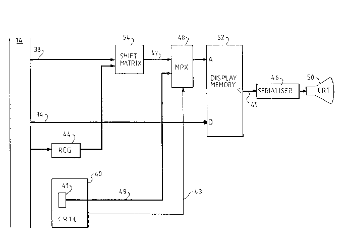
Figure 3 illustrates elements of an example of a
display system in accordance with the invention in the
form of a display adapter. As with the prior art display
adapter illustrated in Figure 2, for reasons of clarity,
only those features which are needed for the skilled
person to understand how to carry out the invention are
illustrated in Figure 3.
The display adapter of Figure 3 is connected to the
system bus 14 of the PC in Figure 1 for receiving the
information to be displayed and information including
mode data controlling the display of that information.
The display information is stored in a display memory, or
frame buffer 52. However, unlike the prior art display
adapter, the display adapter illustrated in Figure 3
comprises a display memory 52 composed of dual-ported
me~ory (here dual-ported video memory, otherwise known as
VRAM). The serial access port S of the VRAM is connected
via a video path 45 to a main picture serialiser 46.
This serial port S is separate from the data port D. The
serial port allows for very fast access to the data in
the memory as long as that data is stored in sequential
storage locations. The aim is thus to ensure that the
display data is stored such that it may read out of the
- UK9-88-018 - 9 - 20 218 2 7
display memory via this serial port S and passed via the
video path 45 to the serialiser for driving the display
device.
The data for updating the display memory are
received at data port D from the system bus via data
lines 34. Unlike the prior art display adapter where the
addresses supplied from the system bus via path 38 are
used unmodified to address the display memory, in the
display adapter illustrated in Figure 3 the addresses may
be modified by a shift matrix 54 in dependence on the
mode data defining the display mode which is placed in
the registers 44 by the PC and supplying the display
data. The mode data in the registers 44 is exactly the
same as that stored in the corresponding registers 44 of
the prior art display system of Figure 2. Thus, in the
case of VGA display systems, the mode data comprises a
bit defining the byte/word mode and a bit defining the
double word mode; these being sufficient to determine the
density with which display data would be stored in the
display memory of a prior art VGA display system. The
address modification defined by the shift matrix 54 for a
given VGA display mode is effectively the inverse of the
address modification which would be performed during
reading of the display memory during active display times
by the shift matrix 42 of the prior art. Thus, whereas
in the prior art display system of Figure 2 single count
increments from the counter 41 are modified by the shift
matrix 42 to steps of 1, 2 or 4 addresses depending on
the display mode, in the display system of Figure 3,
shift matrix 54 generates single address increments from
address steps of 1, 2 or 4 addresses from the system bus
depending on the display mode. In this way the data for
display can be densely stored in the display memory such
that it may be accessed serially at active display times
for all of the required VGA modes.
Given that the display data is densely stored in all
display modes, the addressing of the display memory
during active display times does not need to take account
_ UK9-88-018 - 10 - 2021827
of the current VGA display mode. Thus the control logic,
or CRTC simply needs an address counter for generating
sequential addresses. There is no need for a shift
matrix for modifying the addresses in active display
times in dependence upon the display mode. More
importantly, as the data is now stored densely in
sequential memory locations, the serial port of the
display memory can be used to output the display data at
a sufficiently high data rate to drive high definition
display monitors.
During active display times, therefore, the count of
the address counter 41 forms the addresses for the
display memory in order to access successive items of
display data. At other times, during updating of the
display data in the display memory, the display memory is
addressed on path 47 by the addresses from the system bus
14 on path 38 as modified by the shift matrix 54. A
multiplexer 48, which operates in response to control
signals on the line 43 from the control logic 40, is
provided for selecting between these two sources of
addresses. The provision of the control signals on the
line 43 forms part of the timing functions provided by
the CRTC.
With the display system in Figure 3, the only
possible case where compatibility cannot be maintained is
where the PC stores display data in the display memory in
one VGA mode, changes the VGA mode such that a new
mapping would be required, and then attempts to read the
data in the display memory. Figure 4 illustrates
modifications to the display system of Figure 3 to cope
with even this situation.
In the display system of Figure 4, in addition to
the main display memory 52 which is used for updating the
display, an auxiliary display memory 58 is provided in
which the display data is stored exactly in the form in
which it would have been in a prior display adapter for
the VGA mode in question. In other words, the data is
_~ UK9-88-018 - 11 - 2021827
stored at the density specified by the addresses from the
PC rather than in the densely packed form described with
reference to Figure 3. This auxiliary display memory is
not used for driving the display, but is merely used for
the retrieval of information by the PC should this be
required.
In order that data can be stored in both the main
and auxiliary display memories 52 and 58, a direct
address path 61 is provided from the address bus 38 to
the multiplexer 56. The control logic 60 differs from
the control logic 40 of Figures 2 and 3 in that it is
arranged to produce additional timing signals on the line
51 for causing the data item from the data bus 34 to be
stored twice, once in the main display buffer using the
address from the shift matrix 54 and once in the
auxiliary display memory using the direct address from
the path 59.
The main and auxiliary display memories may be
separate memories, possibly with the auxiliary memory
implemented with DRAM, or some other single ported
memory, or they may be configured as on and off-screen
portions of a single memory.
In the event that the PC stores display data in the
display memory in one VGA mode and then changes the VGA
mode such that a new mapping would be required, data can
be read out from the auxiliary memory 58 and then stored
anew in the main display memory 52 in accordance with the
new mapping defined by the mode data which will have been
stored in the register 44 by the PC. The data transfer
can occur via a data path (not shown) between the
auxiliary memory (58) and the main display memory (52) or
by means of conventional bit-blt operations as
appropriate under the control of the control logic 60.
If an update operation is performed by the PC during the
transfer between the auxiliary and main display memories,
the control logic will temporarily interrupt the transfer
_ UK9-88-018 - 12 - 2 0 2 18 2 7
while the update is performed. As the update information
will be stored in accordance with the new mode data, this
can be done irrespective of the stage the transfer
operation has reached.
Although specific examples of a display system in
accordance with the present invention are described
above, it will be appreciated that many additions and
modifications are possible within the scope of the
attached claims.
For example, although specific examples of display
systems in the form of display adapters are described,
the term display system is not limited thereto. The term
display system is intended to cover any system capable of
displaying data on a display device. Thus the term
applies equally to a display adapter available, for
example, as an add-on card for an existing computer
system such as a personal computer and to a complete
computer system. The display device included in the
display system or to which it may be attached could be a
CRT display, or any other appropriate type of visual
display or printing device.
Although the specific examples relate to the support
of VGA display modes where the display memory is
implemented in dual-ported memory technology (eg. VRAM),
the invention is not limited thereto; it being equally
applicable to other display standards where display
memory format differences occur. Similarly, the
invention could be applied to display systems having
display memories implemented in technologies other than
dual-ported memory technology (eg. VRAM).