Note: Descriptions are shown in the official language in which they were submitted.
2~22127
Background of the Invention
This invention relates to light modulators and, more
particularly, to high-speed light modulators whose operation is based on
varying the electro-optic properties of liquid crystal materials. ;~
S Liquid crystal light modulators are useful in a ~ :~
variety of applications of practical importance. They may, for example,
be employed in a data communication system to modulate a serial stream
of optical pulses. Or such modulators may be arranged in a two-
dimensional array to form a flat panel display. ~ ~
Many available liquid crystal light modulators ~ ~ -
exhibit relatively slow response times. In practice, this property limits the
suitability of such modulators for use in high-bit-rate communication
systems and large-area high-definition displays. ~ ~One of the factors contributing to the slow response ~ -
15 time of liquid crystal light modulators is that most of them as heretofore
proposed respond to a quadratic component of the electric field E, that is,
they are E2 dependent. Once the field (of either polarity) is removed,
the liquid crystal relaxes to its zero-field state. These relaxation times are
typically long and not electrically controllable. ~ ~ .
There are two known references which disclose a
linear or polarity-sensitive electric-field effect in a liquid crystal material.G. E. A. Durand et al in U. S. Patent No. 4,564,266 disclose an electro-
optic device in which different alignment layers are utilized to impose
parallel and perpendicular orientations on the molecules at opposed
25 surfaces of a liquid crystal layer. In operation, the Durand et al device
requires electrodes that are transversely arranged with respect to the
direction of light propagation through the device. For a large-area display
that includes a layer of liquid crystal material that is only, for example,
about 10 micrometers thick, such an electrode array is generally not
30 feasible.
The second known reference that discloses a linear -
electric-field effect in a liquid crystal material is an article by N. V.
Madhusudana et al entitled "Linear Flexo-Electro-Optic Effect In A
Hybrid Aligned Nematic Liquid Crystal Cell", J. Physique Lett.. Vol. 46,
' " ' -- ':'~
' ' ~:~.. :
-`` 2~2~ 2~
- 2 -
:
1985, pages L195-L200. As in the aforecited Durand et al patent,
different alignment layers are utilized to impose parallel and
perpendicular orientations on the molecules at opposed surfaces of a
liquid crystal layer. Due to a bulk effect in the material, the molecular
5 orientation can be altered by applying an electric field perpendicular to
the liquid crystal surfaces. No particular device applications for such an
arrangement are suggested in the article. -
Moreover, in both of the aforecited references,
linear operation is limited to low voltages to avoid dielectric contributions
10 that are polarity-insensitive. Accordingly, the speed of operation of the
devices described therein is relatively slow in the linear region.
Summary of the Invention
In accordance with the principles of the present
invention, asymmetry is established in the interfacial interactions between
15 the surfaces of a liquid crystal material and alignment layers respectively
disposed in contact with the surfaces of the material. Such asymmetry is
introduced in the form of either different anchoring strengths or different
angular tilts of the liquid crystal molecules at the two surfaces.
Accordingly, in either case, in response to the application of an electric
20 fie1d perpendicular to the surfaces of the liquid crystal material, differentcurvatures of the contour of the longitudinal axes of the liquid crystal
mo1ecules are thereby established at the two surfaces. In particular, the
different curvatures of the molecu1ar orientations thereby established at
the two surfaces are each less than about 45 degrees. As a result of this
25 asymmetrical orientation, the flexo-electrically induced net polarization in
the liquid crystal material caused by one polarity of applied field is
different from that caused by the other field polarity. In that way, a
polarity-sensitive electro-optic effect in the liquid crystal material is
realized, thereby providing a basis for fast electrically controlled
3Q operation of a light modulator that includes such a material.
In one embodiment of the invention, different :
anchoring strengths are established at the two surfaces of the liquid crystal -;
material by utilizing two different materials as the alignment layers. In
other embodiments, the same material is used for each of the alignment
35 layers but various techniques such as oblique evaporation, controlled
rubbing or electrical biasing are employed to ensure that molecules at the
two surfaces of the liquid crystal material exhibit different tilt angles.
3 2~ 27
~ef Descri~i~ of the Drawin~s
A complete understanding of the present invention
and of the above and other features and advantages thereof will be
apparent from a consideration of the detailed description set forth below
5 taken in conjunction with the accompanying drawing, not drawn to scale,
in which:
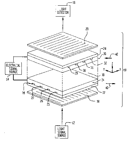
FIG. 1 is a simplified diagrammatic representation
of a light modulator made in accordance with the principles of the present
inventlon; ;
FIGS. 2 and 5 each schematically depict the contours
of the longitudinal axes of liquid crystal molecules included in the FIG. 1 .~ ;
arrangement;
and FIGS. 3 and 4 show the orientation of individual
molecules at the upper and lower surfaces, respectively, of the liquid
15 crystal material contained in the FIG. 2 depiction.
Detailed Description
~ L specific illustrative light modulator 10 made in
accordance with the principles of the present invention is represented in
FIG. 1. Light signals from a source 12 are directed at the bottom surface ~ -
20 of the modulator 10. Electrical signals applied to the modulator 10 from
a source 14 determine the intensity of light delivered by the modulator 10
to a light detector 16. Por a particular value of applied electrical voltage
of one polarity, a maximum-intensity light signal derived from the source
12 is delivered by the modulator 10 to the detector 16. For a particular
25 value of electrical voltage of the other polarity, a minimum-intensity light .
signal is applied to the detector 16. Por intermediate values of applied
electrical signals, other output light intensities can be obtained. For
display applications, this last-mentioned mode of operation provides a so- ~ -
called gray-scale capability. :
The specific illustrative light modulator 10 shown in
PIG. 1 includes conventional polarizer and analyzer plates 18 and 20,
respectively. By way of example, the polarizer plate 18 is designed to ~ -
allow passage therethrough only of those components of the input light
provided by the source 12 that are linearly polarized parallel to the -
35 indicated Y axis. Further, the analyzer plate 20 is designed to allow
passage therethrough only of those components of the light propagating
through the modulator 10 that are linearly polarized parallel to the X axis.
:-~ 2~2~2~ :
- 4 -
Thus, only if the electrical signal applied to the modulator is effective to
modify the polarization of light admitted by the polarizer plate 18 by 90
degrees will virtually all of the admitted light pass through the analyzer
plate 20 and be applied to the detector 16. Illustratively, a positive
S electrical signal of a specified value is effective to cause such a 90-degree
rotation, and a negative electrical signal of a specified value is effective to
ensure that no rotation occurs. In the latter case, virtually all of the light
admitted through the plate 18 will be blocked from passing through the
plate 20 to the detector 16.
The light modulator 10 of FIG. 1 further includes
spaced-apart transparent glass plates 22 and 24. Illustratively, the plates
22 and 24 each have deposited thereon either a continuous electrode or an
array of electrodes. In the particular embodiment represented in PIG. 1,
each of the plates 22 and 24 includes an array of transparent spaced-apart
15 electrodes. Thus, for example, the plate 22 includes electrodes 25 `
through 28, and the plate 24 includes electrodes 29 through 32. As
indicated, the sets of electrodes on the plates 22 and 24 are orthogonally
disposed with respect to each other thereby to form a matrix array of
electrodes. Such an array facilitates electrical control of the depicted
20 modulator by the electrical signal source 14.
Also disposed on each of the plates 22 and 24 of
PIG. 1 is a layer of a so-called alignment material whose nature and ;
function will be described in detail later below. Thus, the plate 22
includes a layer 34 of alignment material, whereas the plate 24 includes a
25 layer 36 of alignment material.
Still further, the light modulator 10 of FIG. 1
inc1udes a layer 38 of liquid crystal material disposed in the space between
the alignment layers 34 and 36. In practice, the layer is, of course
retained in the indicated space by a conventional annular member (not ~
30 shown). Illustratively, the thickness of the layer 38 is only about 10 ;~ -
micrometers. In one particular illustrative embodiment, the layer 38
comprises a standard nematic liguid crystal material having elongated
rod-like molecules characterized by positive dielectric anisotropy.
In one specific embodiment of the invention, the
layers 34 and 36 shown in FIG. 1 respectively comprise different known ;
alignment materials. In particular, each of the alignment materials is
selected to exhibit a different anchoring strength or binding force with : -
202212~ ~ ~
5
respect to the molecules of the liquid crystal material in the layer 38. In
that way, an asymmetrical interfacial interaction is established beeween
the differene alignment materials and the respective opposed surfaces of
the liquid crystal material.
Moreover, in the herein-described specific
embodiment, each of the alignment layers 34 and 36 of FIG. 1 is
advantageously rubbed in a particular fashion to impose a specified
orientation on the molecules of the liquid crystal layer 38. Such rubbing
of alignment layers to control the molecular orientation of liquid crystal . .
10 materials is well known in the art. Illustratively, the layers 34 and 36 are
respectively rubbed in anti-parallel directions in the X-Y plane at an angle ~ .
of about 45 degrees with respect to each of the X and Y axes, as indicated
by arrows 40 and 42 in FIG. 1.
As indicated above, asymmetrical interfacial
15 interactions (different anchoring strengths) are established at the
respective surfaces of the liquid crystal layer 38 of FIG. 1. As a result,
the flexoelectrically induced net polarization in the layer 38 caused by an
electric field applied in the +Z direction is different from that caused by
a field in the -Z direction. This results from the fact that the splay and
20 bending of liquid crystal molecules at one surface are different from those
at the other surface. Consequently, a polarity-sensitive electro-optic
effect is thereby realized in the liquid crystal material.
FIG. 2 is a simplified depiction that indicates the --; .
effect of an applied electric field on the molecules in the liquid crystal
layer 38 of FIG. 1. Lower plate 44 in FIG. 2 schematically represents
both an electrode and an alignment layer, whereas upper plate 46 is a
composite representation of another electrode and an alignment layer
made of a different material characterized by a different anchoring
strength with respect to the molecules of the layer 38.
A voltage of one polarity is assumed to be applied
between the electrodes represented in PIG. 2 thereby to establish an
electric field in the direction of arrow 48 in at least a portion of the liquid
crystal material contained between the plates 44 and 46. In FIG. 2, the
multiple identical curved lines that extend between the plates 44 and 46
35 indicate the contours assumed by the longitudinal axes of the liquid crystal
molecules in response to the applied electric field. As represented, for
example, by the contour line 50, each of the curved lines has a curvature
. .
~`"` 2~22~ 2~
-6-
in the X-Z plane in the upper region of the liquid crystal material that is
different from the curvature in the lower region of the material.
The orientation of liquid crystal molecules in an
upper portion of the FIG.2 depiction adjacent to the plate 46 is shown in :
5 more detail in FIG.3. More specifically, the orientation of molecules
within dash-line box 52 of FIG.2is diagrammatically shown in simplified
form in FIG.3. Each of the liquid crystal molecules represented in the
box 52 of FIG.3is shown as an elongated rod. By way of example, the
longitudinal axes of the molecules in the first row of FIG.3 are each
10 shown as still being approximately parallel to the indicated X axis, due to
the relatively large anchoring strength imposed thereon by the alignment
material included in the upper plate 46 of FIG.2. (In the absence of an
applied field, all the longitudinal axes of the liquid crystal molecules are
approximately parallel to the X axis.) But, as the distance from the plate
15 46 increases, it is apparent from FIG.3 that the applied electric field
gradually overcomes the effect of the anchoring strength. At a point
approximately equidistant between the plaees 44 and 46, the longitudinal
axes of the liquid crystal molecules are approximately parallel to the Z
axis.
Similarly, the orientation of liquid crystal molecules
in a lower portion of PIG.2 adjacent the plate 44 is shown in more detail :
in PIG.4. Specifically, the orientation of molecules within dash-line box -~
54 of PIG.2is diagrammatically shown in FIG. 4. By way of example,
the longitudinal axes of the molecules in the last row of FIG.4 are each -:
25 shown approximately parallel to the indicated X axis, even though the -
anchoring strength imposed on the molecules by the alignment material ~;
included in the lower plate 44is assumed to be small relative to that of
the alignment material in the upper plate 46. But due to this difference in
anchoring strengths, it is apparent from FIG. 4 that molecules near the
30 lower plate 44 are less gradually oriented toward parallelism with the Z
axis as the distance from the plate increases into the bulk the liquid crystal
material than is the case in the FIG. 3 depiction.
FIG.Sis a depiction that is similar to that of FIG.2. ~-
But in PIG.S the direction of the applied electric field is reversed, as
35 indicated by arrow 56. As a result, as represented by the curved lines
shown in PIG.S, the contours of the longitudinal axes of the liquid crystal
molecules again have a curvature in the X-Z plane in the upper region of
c,. , ,,, ;., "'; ~
` ^" 2022127 ~-:
-7-
the liquid crystal material that is different from the curvature in the lower
region of the material. Significantly, however, due to the aforedescribed
asymmetrical interfacial interactions, these different curvatures in the
upper and lower regions of PIG. S are respectively different from the
S curvatures in the lower and upper regions of the arrangement represented
in PIG. 2. Consequently, the net flexoelectrically induced polarization in
FIG. S is different than that produced in the FIG. 2 case. Hence, the
described liquid crystal arrangement exhibits a polarity-sensitive electro-
optic effect.
In one specific illustrative embodiment of the
principles of the present invention, a standard commercially available
liquid crystal material that exhibits the nematic phase at room
temperature is utilized to form the layer 38 of PIG. 1. By way of
example, a liquid crystal material designated E7 available from EM
15 Industries Incorporated, Advance Chemical Division, S Skyline Drive,
Hawthorne, New York 10532, is suitable for this purpose.
In the noted illustrative embodiment, two different
alignment polymers are respectively deposited on the plates 22 and 24
(FIG. 1) to achieve different anchoring strengths with respect to surface
20 regions of the aforespecified liquid crystal material. Thus, for example,
layers of poly (1,4-butylene terephthalate) containing aromatic rings that
resemble the cores of the liquid crystal molecules and nylon 6, 6 which
resembles the tails of the liquid crystal molecules are deposited in
conventional ways on the plates 22 and 24, respectively, and then rubbed
25 in the particular manner previously described above. As a result, the
liquid crystal molecules are thereby aligned with their long axes .
approximately parallel to the arrows 40 and 42 (FIG. 1) and, significantly,
are anchored to the two noted alignment polymers with different
strengths. Illustratively, the difference in anchoring strengths of the
30 aforespecified alignment materials with respect to surface regions of the
specified liquid crystal material is approximately 9.0 x (10 2 10 4) ergs
per centimeter square. -~ ~
In general, a difference in anchoring strengths of at -
least about
35 1 x 10 4 ergs per centimeter square is required in a light modulator made
in accordance with the present invention. In practice, such a difference is
effective to provide the asymmetrical interfacial interactions which
~: :, . . . . . . . .
'` 2~22~27
- 8 -
provide the basis for the herein-described polarity-sensitive control of the
electro-optic properties of a liquid crystal material.
In accordance with the invention, both quiescently
and in the presence of an applied electric field of either polarity, at least
S one layer of liquid crystal molecules at each surface of the layer 38 (~IG.
1) has its longitudinal axes disposed at an angle of about 45 degrees or
less with respect to the X-Y plane depicted in the drawing. In the
particular depictions of FIGS. 3 and 4, this angle is shown as being
approximately 0 degrees.
In accordance with the invention, techniques other
than the one described above based on different anchoring strengths are
available for establishing the asymmetrical interfacial interactions required
for polarity-sensitive operation of a light modulator that includes a liquid
crystal material. These other techniques all cause the longitudinal axes of ~ ~ i
15 molecules at one surface of the liquid crystal material to be quiescently
tilted at an angle that is different from that of the longitudinal axes of the
molecules at the other surface. Both quiescently and in the presence of
an applied electric field, at least one layer of liquid crystal molecules at
each surface has its longitudinal axes thereby disposed at an angle of
20 about 45 degrees or less with respect to the X-Y plane (FIGS. 3 and 4).
By so establishing different tilt angles, these other techniques ensure that
the electro-optic effects caused in the material by an applied electric field
will be asymmetrical with respect to field reversal. In practice, a
difference in tilt angle of about two degrees is adequate to achieve the
25 desired asymmetrical effect. As this difference increases, so too does the ~ -
asymmetrical effect.
One technique for achieving different tilt angles of
the molecules in surface regions of the liquid crystal layer 38 (FIG. 1) ~ - -
involves employing more force during rubbing of one of the alignment
30 layers 34 and 36 than during rubbing of the other layer. Or the same
asymmetrical effect can be achieved by rubbing each of the alignment
layers with the same force but with a different material. In either of
these cases, the same alignment material may be used for the layers 34 - ~
and 36. -
In accordance with the invention, another technique
for achieving different molecular tilt angles involves no rubbing and using
the same alignment material for each of the layers 34 and 36. In this
J~ , , - ~ : . :
. ~:,.,i. ',:~ ' . .. . : ,, ::
' 'r ~
' 2~22~27
g
technique, a material such as silicon oxide is sputtered onto the plate 22
(FIG. 1) at an oblique angle with respect to the indicated X-Y plane and
sputtered onto the plate 24 at a different oblique angle. Deposited
material so oriented is effective to impose different tilt angles on liquid
S crystal molecules at the respective surfaces of the layer 38.
A still further technique is practicable for achieving
different molecular tilt angles. This involves applying a constant direct-
current bias voltage across the liquid crystal layer 38 shown in PIG. 1.
Thus, for example, assume that a bias voltage of -V/3 volts is applied .
10 from the source 14 via an electrode to the top of the layer 38 and that the
bottom of the layer 38 is connected to the source 14 via another electrode
to a point of reference potential such as ground. Asymmetrical interfacial
interactions in the form of different quiescent molecular tilt angles are
thereby established at the two liquid crystal surfaces. Assume further that ~ :
15 a symmetrical control voltage that varies between +V and -V is then
applied across the biased layer 38. As a result of the offset caused by the
bias voltage, an asymmetrical net voltage that varies between + 2V/3 and
-4V/3 will thereby be applied across the layer 38. In turn, the electro-
optic effect produced in the layer 38 is thus different for the positive and
20 negative-going excursions of a bipolar control voltage.
Pinally, it is to be understood that the above-
described procedures and arrangements are only illustrative of the
principles of the present invention. In accordance with these principles,
numerous modifications and al~ernatives may be devised by those skilled
25 in the art without departing from the spirit and scope of the invention.
:, .