Note: Descriptions are shown in the official language in which they were submitted.
20221 92
OPTICAL DISK RECORDING/REPRODUCING DEVICE
FIELD OF THE INVENTION
The present invention relates to an optical disk
recording/reproducing device that records and/or
reproduces information while performing a control such
that a so-called Write-Once type or Rewritable type
optical disk is rotated in Constant Linear Velocity.
BACKGROUND OF THE INVENTION
In the conventional art, compact disks (herein after
referred to as CDs) whereon audio information or other
information is recorded in the form of digital signals
through minute pits that can be detected optically, are
widely used as optical disks. The information recorded on
a CD is reproduced by means of a Read-Only optical disk
recording/reproducing device.
2022 1 92
In a CD, a plurality of pieces of information are
usually recorded in succession. In addition, absolute
addresses that provide information concerning
recording/reproducing positions on the disk are
preliminary recorded on the disk in the form of physical
alterations. During the reproduction, absolute addresses
read from the disk and absolute addresses indicating the
recording start position of each piece of information and
recorded in a TOC (Table of Contents) area provided in the
inner periphery or other location of the disk, are
compared,- and the desired pieces of information may be
reproduced success1vely or selectively.
An optical disk recording/reproducing device that
records and reproduces audio information or other
information on rewritable optical disks developed recently
such as magneto-optical disks or Write-Once type optical
disks where information can be recorded only once, should
preferably adopt the same method of reproduction as the
one used in a conventional optical disk
recording/reproducing device for CDs only and should be
able to be employed compatibly with the different types of
optical disks in use. In this case, a so-called Constant
Linear Velocity (hereinafter referred to CLV) that is
employed with CDs may be adopted as rotation control
method for the optical disk during the recording and the
~2~!92
reproduction.
The CLV method may be implemented by for example
controlling the rotational speed of a motor in accordance
with the radial position of an optical head. In this case,
the rotational speed of the motor is detected by means of
a rotary encoder or other member, and the radial position
of the optical head is detected by means of a position
detecting sensor. However, when the CLV method is
implemented in such a manner, a rotation control that is
sufficiently accurate cannot be expected as errors occur
in, for instance, the detections performed by the rotary
encoder and the position detecting sensor.
The accuracy of the rotation control may be improved
by enforcing the CLV method according to disk position
information that was preliminary recorded on the optical
disk such as the absolute addresses described above. In
the conventional art, Japanese Publication for Unexamined
Patent Application 1989-39632 (Tokukaisho 64-39632)
discloses a method for recording absolute addresses.
Namely, the disk position information goes through a
Biphasemark modulation process and the guiding groove of
the optical disk is made to deviate inward or outward in a
radial direction or the width of the guiding groove is
changed, depending on whether the modulated code is "1" or
"O". The absolute addresses and the recorded information
2022 1 92
can be reproduced separately by having their respective
frequency bandwidths differ from each other.
However, even if the information is recorded while
the optical disk is driven to rotate according to the
information preliminary recorded on the optical disk such
as absolute addresses, etc., in practice, there is a
possibility that the information might be recorded in a
condition that is slightly different from the CLV
requirements because of CLV control errors happening
during the recording. In this case, if the information
recorded is audio information, variations might occur in
the speed at which music is played during the
reproduction. Therefore, during the reproduction, a CLV
control that is based on the information to be reproduced
should be performed.
However, when during the reproduction, reproduction
errors occur frequently, or when the optical head moves
from a recorded area to an unrecorded area, a rotation
control that is based on the reproduced information
becomes infeasible. In addition, once the rotation control
based on the reproduction information has become
infeasible, a significant lapse of time is needed before
the rotation control can be executed correctly even after
the quality of the reproduced signals was restored.
- 2022~92
SUMMARY OF THE INVENTION
An object of the present invention is to provide an
optical disk recording/reproduclng device where the
rotation control in Constant Linear Velocity of an optical
disk, may be executed based on the reproduced signals of
pre-recorded information that was preliminary recorded on
the optical disk, during the reproduction when a rotation
control based on the reproduced signals of recorded
information is infeasible.
In order to achieve the above object, an optical disk
recording/reproducing device in accordance with the
present invention is characterized in comprising-control
means for performing the rotation control of an optical
disk in Constant Linear Velocity such that:
during the recording, the rotation control is
executed according to reproduced signals of pre-recorded
information that was recorded on the optical disk
preliminary,
during the reproduction, the rotation control is
executed according to reproduced signals of recorded
informatlon, and
when the rotation control based on the reproduced
signals of the recorded information is infeasible, the
rotation control is switched and executed according to the
reproduced signals of the pre-recorded information during
6 --
2G22~92
the reproduction also.
With the above arrangement, the rotation control in
Constant Linear Velocity (CLV) is performed according to
the reproduced slgnals of the pre-recorded information
during the recording, and according to the reproduced
signals of the recorded information during the
reproduction. As a result, a suitable and appropriate CLV
control may be performed during the recording and the
reproduction.
In addition, when during the reproduction, the CLV
control based on the reproduced signals of the recorded
information is infeasible because of reproduction errors
happening frequently, or because reproduced signals cannot
be obtained as the optical head entered into a unrecorded
area, an alternative method can be followed. With this
alternative method, the CLV control is switched to the CLV
control based on the reproduced signals of pre-recorded
information during the reproduction also. Difficulties
such as the infeasibility of a CLV control during the
reproduction, may be thus overcome.
For a fuller understanding of the nature alld
advantages of the invention, reference should be made to
the ensuing detailed description taken in conjunction with
the accompanying drawings.
- 20221 92
BRIEF DESCRIPTION OF THE DRAWINGS
Fig. 1 to Fig 6 illustrate a first embodiment of the
present invention.
Fig. l(a) is a flow chart illustrating a CLV control
procedure during a recording.
Fig. l(b) is a flow chart illustrating a CLV control
procedure during a reproduction.
Fig. 2 is a schematic plane view illustrating a
magneto-optical disk.
Fig. 3 is an enlarged partial plane view illustrating
the magneto-optical disk.
Fig. 4 is a block diagram illustrating schematically
the configuration of an optical disk recording/reproducing
device.
Fig. 5 is an explanatory view illustrating the frame
format of a signal.
Fig. 6 is a block diagram illustrating essential
parts of the optical disk recording/reproducing device.
Fig. 7 is a block diagram illustrating essential
parts of an optical recording/reproducing device of a
second embodiment.
Fig. 8 to Fig. 11 illustrate a third embodiment.
Fig. 8 is a block diagram illustrating essential
parts of an optical disk recording/reproducing device.
Fig. 9 to Fig. 11 are time charts respectively
20221 92
illustrating the variation of signals around a phase
locked loop.
Fig. 12, Fig. 13, and Fig. 14 are block diagrams
respectively illustrating essential parts of optical disk
recording/reproducing devices of a fourth, a fifth and a
sixth embodiment.
Fig. 15 and Fig. 16 illustrate a seventh embodiment.
Fig. 15(a) is a flow chart illustrating a CLV control
procedure during a recordlng.
Fig. 15(b) is a flow chart illustrating a CLV control
procedure during a reproduction.
Fig. 16 is a block diagram illustrating schematically
the configuration of another optical disk
recording/reproducing device.
DESCRIPTION OF THE EMBODIMENTS
A first embodiment of the present invention will be
described with reference to Fig. 1 to Fig. 6.
As illustrated in Fig. 2, a magneto-optical disk 1 as
a rewritable optical disk, is accommodated with a TOC
(Table Of Contents) area la located in the inner
periphery, as well as with an information recording area
lb occupying most of the area outside the TOC area la.
Different types of information such as music programs or
other data, are recorded in the information recording area
2~22~ 92
lb while additional information concerning the different
pieces of information recorded in the information
recording area lb, is recorded in the TOC area la. The
additional information might consist for example of
absolute addresses indicating the recording start position
and absolute addresses indicating the recording end
position of each lnformation.
As illustrated in Fig. 3, a guiding groove 2 of a
spiral shape (shown by hatching for reasons of
convenience) is preliminary formed in the TOC area la and
the information recording area lb of the magneto-optical
disk 1 and circles at predetermined intervals in a radial
direction. The guiding groove 2 may also be composed of
concentric circles. The guiding groove 2 is used for the
tracking control during the recording and the
reproduction. The guiding groove 2 is made to deviate
inward or outward in a radial direction depending of
whether the modulated codes obtained after the absolute
addresses provided on the disk went through a Biphasemark
modulation process, are "1" or "O". The above absolute
addresses form pre-recorded information to be used as
rotation control information.
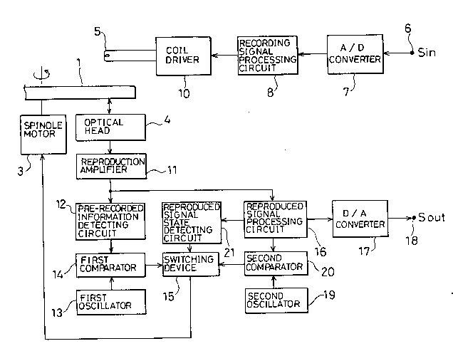
As illustrated in Fig. 4, the optical disk
recording/reproducing device of the present embodiment
comprises a spindle motor 3, as driving means for
-- 10 --
20221 92
supporting and driving the magneto-optical disk 1 to
rotate, an optical head 4 that projects a laser beam on
the magneto-optical disk 1 during the recording and the
reproduction, and a coil 5 that applies a magnetic field
on the magneto-optical disk 1 during recording. The
present optical disk recording/reproducing device adopts a
magnetic modulation method as method for recording
information and is capable of overwriting by recording new
information over information already recorded.
The optical disk recording/reproducing device
includes an input terminal 6 where the information to be
recorded is entered to. An analog information that was
entered through the input terminal 6 is converted into a
digital signal in an A/D (analog/digital) converter 7,
goes through a prescribed EFM (Eight to Fourteen
Modulation) process in a recording signal processing
circuit 8, and is fed into a coil driver 10. The signal is
recorded as the coil driver 10 drives the coil 5 in
response to the signal that was fed thereto, while at the
same time a laser beam is projected from the optical head
4 and is irradiated on the magneto-optical disk 1.
Fig. 5 shows the frame format of signals used in a
CD. An information "a" of one frame is composed of a data
field "d" comprising an audio information or other
information of 24 bytes and an error correction parity of
2û22~92
8 bytes added thereto, a sub code "c" indicating the
number of the piece of music, the time and other
information about the audio information, and a
synchronlzing signal "b" appended to each frame and
indicating the leading edge of the frame. Pieces of
information "a" of one frame are recorded in succession.
Sub codes "c" comprised in the pieces of additional
information recorded in the TOC area la further include at
least information concerning the recording end position of
each information, or information indicating the recording
time from the recording start position to the recording
end position of each information recorded according to the
above frame format.
The reproduction system of the optical disk
recording/reproducing device will be described
hereinbelow. As illustrated in Flg. 4, a signal that was
reproduced by means of the optical head 4 is amplified by
a reproduction amplifier 11. The signal that was amplified
is sent to a pre-recorded information detecting circuit 12
and to a reproduced signal processing circuit 16.
The pre-recorded information detecting circuit 12 is
for example composed of a band-pass filter and a phase
locked loop. Clock signals that are synchronized with the
reproduced signals of the pre-recorded information (that
is, constituted by a Biphasemark modulated wave) that were
20221 92
extracted from the reproduced signals by means of the
band-pass filter, are generated by the phase locked loop.
The frequency of the clock signals and a first reference
frequency supplied by a first oscillator 13 are compared
in a first comparator 14 and differential signals are fed
lnto a switching device 15. The present device further
comprises a pre-recorded information demodulating section,
not shown. When necessary (for instance when accessing,
etc.), the Biphasemark modulated waves go through a
Biphasemark demodulation process in the pre-recorded
information demodulating section, thereby permitting the
absolute addresses to be recognized.
Magneto-optical signals that were extracted from the
reproduced signals supplied from the reproduction
amplifier 11, i.e. the reproduced signals of the recorded
information, go through a process for demodulating the
signals that were modulated through an EFM process, and
other prescribed processes in the reproduced signal
processing circuit 16. After the signals passed through
these reproduction processes, they are released outside
across a D/A (digital/analog) converter 17 and an output
terminal 18.
The frame synchronizing signals described earlier
comprised in each of the frames composing the reproduced
signals of the recorded information are detected by means
- 13 -
2022192
of the reproduced signal processing circuit 16. When a
synchronizing signal is detected, a synchronizing signal
detection pulse is generated by the reproduced signal
processing circuit 16 and sent to a second comparator 20.
The frequency of the synchronizing signal detection pulse
is compared with a second reference frequency supplied
from a second oscillator 19 and the differential signal
resulting from this comparison is sent to the switching
device 15. When the same reference frequency is employed
in the first oscillator 13 and the second oscillator 19, a
common oscillator may be used for the first oscillator 13
and the second oscillator 19. Also, when the first and
second reference frequencies of the first and second
oscillators are such that one frequency equals an integer
number of times the other, a single oscillator may be used
and the frequency of this oscillator divided appropriately
by means of a divider.
The signals that were processed in the reproduced
signal processing circuit 16, are sent to a reproduced
signal state detecting circuit 21 serving as reproduced
signal state detecting means. In the signal state
detecting circuit 21, it is determined whether the
magneto-optical signals recorded on the magneto-optical
disk 1 are reproduced correctly, or whether the optical
head 4 is presently reproducing a recorded area or an
- 14 -
- 202~92
unrecorded area. Namely, the reproduced signal state
detecting circuit 21 detects that frame synchronizing
signals are successively missing due to anomalies in the
synchronization, or that frame synchronizing signals are
successively missing because the optical head 4 entered
into an unrecorded area.
The optical disk recording/reproducing device further
comprises control means composed of a controller and other
members, not shown. As illustrated in Fig. l(a), during
recording, the control means switches the switching device
toward the first comparator 14 and executes the
recording operation (S2) while performing the CLV control
according to the reproduced signals of the pre-recorded
information (S1). The CLV control is performed such that
the differential signals released by the first comparator
14 are sent to the spindle motor 3 through the switching
device 15 and the frequency of the clock signals released
by the pre-recorded information detecting circuit 12
coincides with the first reference frequency of the first
oscillator 13. The clock signals are synchronized with the
Biphasemark modulated waves of the absolute addresses
serving as pre-recorded information.
As illustrated in Fig. l(b), during reproduction, the
condition of the reproduced signals is detected by means
of the reproduced signal state detecting circuit 21 (S11)
- 15 -
2 022 1 92
and the control means determines whether the reproduced
signals are in a suitable condition (S12). When the
reproduction of a recorded area is performed and when the
reproduced signals are in a suitable condition, the
control means switches the switching device 15 toward the
second comparator 20 and executes the reproduction
operation while performing the CLV control according to
the reproduced signals of the recorded information (S13).
In this case, the CLV control is performed such that, the
differential signals released by the second comparator 20
are fed into the spindle motor ~ through the switching
device 15 and the frequency of the synchronizing signal
detection pulses released from the reproduced signal
processing circuit 16 coincides with the second reference
frequency of the second oscillator 19. As a result, the
amount of information reproduced per time unit during the
reproduction is kept constant even when slight variations
occurred in the linear velocity during recording.
As described earlier, during the reproduction, an
alternative method is followed when the CLV control based
on the reproduced signals of the recorded information is
infeasible, that is when the reproduced signal state
detecting circuit 21 detects that the optical head 4
entered into an unrecorded area, or that reproduction
errors occur frequently and that the condition of the
- 16 -
20221 92
reproduced signals deteriorated. The alternative method
consists in switching to a CLV control executed based on
the reproduced signals of the pre-recorded information
during reproduction also (S14). Inconveniences such as the
infeasibility of a CLV control during the reproduction,
are thus eliminated.
The configuration and operation of the reproduced
signal state detecting circuit 21 will be described more
precisely hereinbelow. As illustrated in Fig. 6, the
reproduced signal state detecting circuit 21 comprises a
counter 22, a comparator 23 and a reference value supply
circuit 24. Synchronizing signal detection pulses, that
are released when frame synchronizing signals are detected
in the reproduced signal processing circuit 16, are fed
with a predetermined timing into a reset terminal of the
counter 22. Meanwhile, synchronizing signal absence pulses
that are released when frame synchronizing signals are
missing in the reproduced signal processing circuit 16,
are fed lnto a clock terminal of the counter 22 with a
predetermined timing. In such a manner, the number of
times a synchronizing signal absence pulse is supplied is
counted by the counter 22. Provision is made such that the
counter 22 is reset when a synchronizing signal detection
pulse is fed thereto.
The value released by the counter 22 is compared with
2~22~92
a reference value supplied by the reference value supply
circuit 24 in the comparator 23. When the value released
by the counter 22 is greater than the reference value, in
other words when frame synchronizing signals are
continuously missing in a number exceeding a predetermined
number, it is determined that a synchronization anomaly
occurred in the recorded area, or that the optical head 4
entered into an unrecorded area and that frame
synchronizing signals cannot be detected while the CLV
control is executed according to the reproduced signals of
the recorded information. A CLV control switch signal is
subsequently released by the comparator 23 and is fed into
the switching device 15. In such a manner, an optical disk
recording/reproducing device in accordance with the
present invention is designed such that during the
reproduction also, the CLV control can be switched from
the CLV control based on the reproduced signals of the
recorded information to the CLV control based on the
reproduced signals of the pre-recorded information. A
suitable and appropriate CLV control is thus ensured
during the recording as well as during the reproduction.
A second embodiment will be described hereinafter
with reference to Fig. 7. The optical disk
recording/reproducing device of the second embodiment has
almost the same configuration as the optical disk
- 18 -
2~22~92
recording/reproducing device of the first embodiment
except that it comprises a reproduced signal state
detecting circuit 21 which configuration and operation is
different from the one described in the first embodiment.
To simplify, only the detailed configuration of another
example of reproduced signal state detecting circuit 21
will be discussed hereinbelow. In this embodiment too,
provision is made such that during the reproduction, the
reproduced signal state detecting circuit 21 switches to
the CLV control executed based on the reproduced signals
of the pre-recorded information when reproduction errors
occur continuously in the recorded area of the information
recording area lb.
As illustrated in Fig. 7, the reproduced signal state
detecting circuit 21 comprises an inverter 25, two NAND
circuits 26 and 27, a counter 28, a comparator 30 and a
reference value supply circuit 31. The above-mentioned
synchronizing signal detection pulses are supplied from
the reproduced signal processing circuit 16 to an input
terminal of the NAND circuit 26 and an input terminal of
the NAND circuit 27. An error flag indicating whether or
not reproduction errors occurred within the frames of the
reproduced signals, is released from the reproduced signal
processing circuit 16 and fed into the other input
terminal of the NAND circuit 26 through the inverter 25.
2 0 2 2 1 9 2
The error flag is fed directly into the other input
terminal of the NAND circuit 27. When a reproduction error
occurred, the error flag released by the reproduced signal
processing circuit 16 is in the high level. On the other
hand when there is no reproduction error, the error flag
released by the reproduced signal processing circuit 16 is
in the low level.
Accordingly, when a reproduction error occurred in a
certain frame and the error flag changes to the high
level, the value of the counter 28 is lncreased in
response to a signal released by the NAND circuit 27 and
fed into the clock terminal of the counter 28. When there
is no reproduction error in a certain frame and the error
flag changes to the low level, the counter 28 is reset in
response to a signal released by the NAND circuit 26 and
fed into the reset terminal of the counter 28. The value
of the counter 28 1s compared w1th the reference value of
the reference value supply circuit 31 in the comparator
30. When the value of the counter 28 is greater than the
reference value, in other words, when reproduction errors
occurred continuously in a number of frames exceeding a
prescribed number, it is considered that reproduction
errors occurred frequently and that the condition of the
reproduced signals deteriorated. A CLV control switch
signal is subsequently released by the comparator 30 and
- 20 -
2~22192
is fed into the switching device 15. As a result, the CLV
control is executed according to the reproduced signals of
the pre-recorded information during the reproduction also.
Another embodiment of the reproduced signal state
detecting circuit 21 will be described with reference to
Fig. 8 to Fig. 11.
As lllustrated in Fig. 8, in this third embodiment,
it is determined by means of the reproduced signal state
detecting circuit 21 whether a phase shift occurs in a
phase locked loop 35 included in the reproduced signal
processing circuit 16. Provision is made such that when a
phase shift occurs, the CLV control is switched.
The reproduced signal processing circuit 16 comprises
a phase locked loop (PLL) 35 composed of a phase comparing
circuit 32, a low-pass filter (LPFJ 33 and a voltage
controlled oscillator (VcO) 34. Meanwhile the reproduced
signal state detecting circuit 21 comprises an edge
detecting circuit 36, a delay circuit 37, a D type
flip-flop 38, a frequency determination section 40 and an
AND circuit 41. The edge detecting circuit 36, the delay
circuit 37 and the flip-flop 38 form a phase determination
section 42.
A binary reproduced signal I is released by the
reproduced signal processing 16 and fed into the edge
detecting circuit 36. Bump edges produced by the
2022 1 92
transitions between the low level corresponding to "O" and
the high level corresponding to "1" of the binary
reproduced signal I, are detected in the edge detecting
circuit 36, and an edge signal II that falls in
synchronization with each bump edge is fed into a clock
input terminal CK of the flip-flop 38. A clock signal III
released by the VCO 34 is fed into the delay circuit 37
where its cycle is delayed by 1/4 of a cycle. A delayed
signal IV obtained as the clock signal III is delayed in
the delay circuit 37, is sent to the data input terminal D
of the flip-flop 38. Furthermore, a phase determination
signal V released from the output terminal Q of the
flip-flop 38, and a frequency determination signal VI
released by the frequency determination section 40 are fed
into the AND circuit 41.
The phase determination signal v is in the high level
when there is no phase difference in the PLL 35 and the
frequency determining signal VI is in the high level when
the frequency of the clock signal III is correct.
Provision is made such that the CLV control is switched
when the CLV control switch signal released by the AND
circuit 41 is in the low level. In addition, the frequency
determination section 40 is designed such as to determine
whether the frequency of the clock signal III is comprised
within a proper range.
- 22 -
2Q22~2
Time charts of the signals I to V in the phase
determination section 42 are illustrated in Fig. 9 to Fig.
11. In the figures, (a) to (e) represent the variations of
the binary reproduced signal I, the edge signal II, the
clock signal III, the delay signal IV and the phase
determination signal V respectively.
Fig. 9 illustrates a case where the PLL 35 is in a
locked condition and the binary reproduced signal I and
the clock signal III are in phase. As it appears clearly
when (b) and (d) of Fig. 9 are compared, the delay signal
IV is always in the high level when the edge signal II
falls whereby the phase determination signal V released by
the flip-flop 38 is always in the high level. At this
time, if in the frequency determination section 40 it is
determined that the frequency of the clock signal III is
comprised within a proper range and the frequency
determination signal VI is in the high level, the CLV
control switch is not performed.
Next, a case where the phase of the clock signal III
of the phased locked loop 35 lags behind is illustrated in
the time chart of Fig. 10. As shown by (c) in Fig. 10, the
clock signal III lags behind the binary reproduced signal
I by approximately two-fifth of a cycle. As a result, the
delay signal IV is always in the low level when the edge
signal II falls whereby the phase determination signal V
- 23 -
2 022 1 92
is always in the low level also. This causes the CLV
control switch signal released by the AND circuit 41 to be
in the low level and the switch of the CLV control to be
executed.
Further, the time chart of Fig. 11 illustrates a case
where the phase of the clock signal III of the phase
locked loop 35 is leading. In this case, the clock signal
III, as shown by (c) in Fig. 11, is ahead of the binary
reproduced signal I by approximately two-fifth of a cycle.
As a result, the delay signal IV is always in the low
level when the edge signal II falls, whereby the phase
determination signal V is always in the low level also. In
this case too, the CLV control switch signal released by
the AND circuit 41 is in the low level and the switch of
the CLV control is executed.
Still another embodlment of the reproduced signal
state detecting circuit 21 will be described with
reference to Fig. 12.
The present fourth embodiment is effective when a
D.C. free modulation method is adopted. The D.C. free
modulation method is a modulation method where the signal
format used is such that there is no difference between
the average level and the zero level of the binary
reproduced signals, i.e. when the energy densities of "1"
and "O" are both approximately equal to 50%. Whether the
- 24 -
2022 1 92
reproduced signals are in an appropriate condition is
determined in the reproduced signal state detecting
circuit 21. If the condition of the reproduced signals is
poor, the CLV control is changed to the CLV control
executed according to the reproduced signals of the
pre-recorded information.
As illustrated in Fig. 12, binary reproduced signals
released from the reproduced signal processing circuit 16
are fed into one of the input terminals o a NAND circuit
43 and are fed into one of the input terminals of a NAND
circuit 45 through an inverter 44. Pulses sent from an
oscillator 46 is entered in the other input terminal of
the NAND circuit 43 and the other input terminal of the
NAND circuit 45. Output signals released by the NAND
circuit 43 are fed into an addition input terminal of an
updown (U/D) counter 47 while output signals released by
the NAND circuit 45 are fed into the subtraction input
terminal of the updown counter 47. With such an
arrangement, if, when a pulse is entered from the
oscillator 46, the binary reproduced signal is in the high
level corresponding to "1", the updown counter 47 counts
up. Meanwhile, if the binary reproduced signal is in the
low level corresponding to "O" when a pulse is entered
from the oscillator 46, the updown counter 47 counts down.
The value released by the updown counter 47 is compared
25 -
~022~2
with a reference value supplied from a reference value
supply circuit 50 in a comparator 48. When the value
obtained in the updown counter 47 is greater than the
reference value, it is assumed that anomalies arose in the
energy densities of "1" and "O" of the binary reproduced
signals and that the condition of the reproduced signals
deteriorated. The comparator 48 consequently releases a
CLV control switch signal.
Another embodiment of the reproduced signal state
detecting circuit 21 will be described hereinbelow.
The optical dlsk recording/reproducing device of the
present fifth embodiment is designed such that, when
during the reproduction the optical head 4 entered into an
unrecorded area of the information recording area lb, the
CLV control is switched to the CLV control executed
according to the reproduced signals of the pre-recorded
information.
As illustrated in Fig. 13, the reproduced signal
state detecting circuit 21 comprises an envelope detecting
circuit 51 and a comparator 52. An analog reproduced
signal before it is converted into a binary reproduced
signal, is released from the reproduced signal processing
circuit 16 shown in Fig. 4 and fed into the envelope
detecting circuit 51.
With the above arrangement, the envelope detection of
- 26 -
20221 92
the analog reproduced signal is performed in the envelope
detecting circuit 51. The voltage of the output signal
obtained after the detection, is compared with a reference
voltage Vc in a comparator 52. When the optical head 4 is
positioned over an unrecorded area where no reproduced
signal is detected, the voltage of the envelope detection
signal is below the reference voltage VC. As a result, the
CLV control switch signal released by the comparator 52
changes to the low level causing the CLV control to be
switched to the CLV control based on the reproduced
signals of the pre-recorded information during the
reproduction also.
Next, description will be made of another embodiment
of the reproduced signal state detecting circuit 21.
In this sixth embodiment also, the optical disk
recording/reproducing device is designed such that, when
during the reproduction the optical head 4 is positioned
over an unrecorded area, the CLV control is switched to
the CLV control executed according to the reproduced
signals of the pre-recorded information.
As illustrated in Fig. 14, the reproduced signal
state detecting circuit 21 comprises an edge detecting
circuit 53 and a re-triggerable monostable multivibrator
54. Two-value reproduced signals released from the
reproduced signal processing circuit 16, are fed into the
- 27 -
20221 92
edge detecting circuit 5~. The time constant of the
re-triggerable monostable multivibrator 54 is set so as to
be, for example, slightly longer than the maximum length
separating two edges of a binary reproduced signal shown
by (b) in Fig. 9. The maximum distance separating two
edges of a binary reproduced signal corresponds, for
example, to 11 bits in an EFM signal. As a result, when
the optical head 4 is positioned over a recorded area of
the information recording area lb, and binary reproduced
signals are entered into the edge detecting circuit 53,
the re-triggerable monostable multivibrator 54 is
triggered in a repetitive manner and thereby releases a
signal that is constantly in the high level. In this case,
the CLV control is not changed.
On the other hand, when the optical head 4 is
positioned over an unrecorded area and no binary
reproduced signal is entered in the edge detecting circuit
53, the detection of edges does not take place.
Accordingly, the re-triggerable monostable multivibrator
54 is not triggered and releases a low level CLV control
switch signal, causing the CLV control to be switched to
the CLV control executed according to the pre-recorded
information during the reproduction also.
A seventh embodiment of the present invention will be
described hereinbelow with reference to Fig. 15 and Fig.
- 28 -
2022 1 92
16. For reasons of convenience, the members having the
same functions than in the previous embodiments will be
designated by the same code and their description will be
omitted.
As illustrated in Fig. 16, the optical disk
recording/reproducing device of the present embodiment
differs from the optical disk recording/reproducing
devices of the previous embodiments in that it is not
equipped with the reproduced signal state detecting
circuit 21. Fig. 16 shows an address decoder 55, a TOC
memory 56 and a controller 57 that are always part of the
optical disk recording/reproducing device.
The address decoder 55 decodes the sequences of data
of the absolute addresses that went through the
Biphasemark demodulation process described earlier. The
absolute addresses are recognized in the controller 57
based on the results obtained in the address decoder 55.
The address decoder 55 and a TOC memory 56 constitute an
address management section.
During the recording, the absolute addresses
indicating recording start positions and the absolute
addresses indicating recordiny end positions mentioned
earlier (hereinafter referred to as recording start/end
absolute addresses) are read from the TOC memory 56 by
means of a recording/reproduction control section (not
` - 29 -
2022 1 92
shown) comprised in the controller 57. The coil driver 10
drives the coil 5 and the optical head 4 to access the TOC
area la in response to the instruction of the
recording/reproduction control section. This instruction
is based on the absolute addresses supplied by the
pre-recorded information detecting circuit 12 and the
address decoder 55. In such a manner, the recording
start/end absolute addresses are recorded in the TOC area
la after going through a prescribed signal process in the
recording signal processing circuit 8.
On the other hand, during the reproduction, the
recording start/end absolute addresses recorded in the TOC
area la are stored in the TOC memory 56 of the address
management section following the instruction of the
recording/reproduction control section. Besides, absolute
addresses processed and detected one after another in the
pre-recorded information detecting circuit 12, are also
fed into the TOC memory 56. The recording start/end
absolute addresses and the absolute addresses detected one
after another are compared in a comparison section (not
shown) included in the controller 57. According to the
result of the comparison, the comparison section
determines whether the optical head 4 is reproducing a
recorded area or an unrecorded area of the information
recording area lb.
- 30 -
2022 1 92
A recording control operation that follows the flow
illustrated in Fig. 15(a) and that is performed by control
means composed of the controller 57 and other members will
be described hereinbelow. First, a switch control section
of the controller 57 (not shown) switches the switching
device 15 toward the first comparator 14. Consequently,
the CLV control of the spindle motor 3 is executed based
on the reproduced signals of the pre-recorded information
(S21). When the recording of audio information or other
information starts, the corresponding recording start
absolute address 1s stored in the TOC memory 56 (s22).
When the recording of the audio information or other
information is completed, the corresponding recording end
absolute address is also stored in the TOC memory 56
(S23). Then, the recording start/end absolute addresses
are recorded as additional information in the TOC area la
of the magneto-optical disk 1 as described earlier (S24).
On the other hand, during the reproduction of
signals, the control means switches the switching device
15 toward the comparator 20 permitting the CLV control of
the spindle motor ~ to be performed according to the
reproduced signals of the recorded information. A
reproduction control operation performed by the control
means that follows the flow illustrated in Fig. 15(b) will
be described hereinbelow. During the reproduction of
- 31 -
20221 92
signals, first, preceding the reproduction of the signals,
the additional information written in the TOC area la is
reproduced, and the recording start/end absolute addresses
are read through the reproduced signal processing circuit
16 and stored in the TOC memory 56 (S31). Next, the
absolute addresses obtained one after another as the
pre-recorded information preliminary recorded on the
magneto-optical disk 1 is reproduced, are compared with
the recording start/end absolute addresses stored in the
TOC memory 56 (s32). Then, it is determined whether the
optical head 4 is located over a recorded area or an
unrecorded area (S33). For instance, if the absolute
addresses reproduced one after another, are greater than
the recording start absolute address and smaller than the
recording end absolute address, it is assumed that the
optical head 4 is located over a recorded area.
Accordingly, the switching device 15 stays connected to
the second comparator 20 and the CLV control is performed
based on the reproduced signals of the recorded
information (S34). On the other hand, when the absolute
addresses reproduced one after another are smaller than
the recording start absolute address, or greater than the
recording end absolute address, it is determined that the
optical head 4 is positioned over an unrecorded area. The
switching device 15 is consequently switched from the
2 ~ 9 2
second comparator 20 to the first comparator 14. As a
result, the CLV control changes from the CLV control
executed according to the reproduced signals of the
recorded information to the CLV control executed according
to the reproduced signals of the pre-recorded information
(s~5).
Accordingly, in the cases where a CLV control
executed according to the reproduced signals of the
recorded information is infeasible such as for example
when the optical head 4 entered into an unrecorded area,
an alternative method that consists in performing the CLV
control based on the reproduced signals of the
pre-recorded information during the reproduction also, is
employed. Inconveniences such as the infeasibility of the
CLV control during the reproduction, are thus eliminated.
Moreover, in the present seventh embodiment, whether the
optical head 4 is positioned over a recorded or unrecorded
area, is determined by merely comparing the absolute
addresses. There is thus no need to implement an
additional detecting means and the configuration of the
circuit may be simplified.
In the above embodiments, the absolute addresses
recorded on the magneto-optical disk 1 went through a
Biphasemark modulation process. However, these are not
restrictlve examples, and other modulation methods that
2022 1 92
restrict the frequency bandwidth may be adopted.
Also, in the above embodiments, the magneto-optical
disk was taken as an example of optical disk. However, the
present invention may be applied to other Rewritable
optical disks such as optical disks of the phase change
type, or to Write-once type optical disks.
Further, in the above embodiments, the absolute
addresses serving as pre-recorded information were
recorded on the optical disk by having the guiding groove
2 deviate. The absolute addresses may also be recorded on
the optical disk in the form of aligned pits. In this
case, the CLV control based on the reproduced signals of
the pre-recorded information is carried out by comparing
the cycle at which the pits are reproduced, with a
predetermined reference frequency.
Furthermore, the above embodiments described a case
where the pre-recorded information is recorded on the
optical disk in the form of absolute addresses. However,
the pre-recorded information may also be recorded by
having the guiding groove 2 snake.
In addition, in the above embodiments, the unrecorded
areas represented areas of the information recording area
lb that were not recorded. However, the present invention
may be applied to for example unnecessary areas such as
blank spaces or unstable recorded areas of recorded areas.
- 34 -
.
20221 92
As described above, an optical disk
recording/reproducing device in accordance with the
present invention comprises control means for executing
the rotation control of an optical disk in Constant Linear
Velocity such that:
during the recording, the rotation control is carried
out based on the reproduced signals of pre-recorded
information that was preliminary recorded on the optical
disk,
during the reproduction, the rotation control is
carried out based on the reproduced signals of recorded
information, and
when the rotation control based on the reproduced
signals of the recorded information is infeasible, the
control is switched to the rotation control based on the
reproduced signals of the pre-recorded information during
the reproduction also.
With the above arrangement, the rotation control in
Constant Linear Velocity is carried out according to the
reproduced signals of the pre-recorded information during
the recording, and based on the reproduced signals of the
recorded information during the reproduction. This
arrangement enables an appropriate and suitable rotation
control to be performed during the recording and during
the reproduction.
- 35 -
- 2022 1 92
In addition, when during the reproduction the
rotation control based on the reproduced signals of the
recorded information is infeasible because reproduction
errors occur frequently, or because reproduced signals
cannot be obtained as the optical head entered into an
unrecorded area, an alternative method can be adopted. The
alternative method consists in switching and executing the
rotation control according to the reproduced signals of
the pre-recorded information. Difficulties such as the
infeasibility of the CLV control during reproduction, may
be thus eliminated.
The invention being thus described, it will be
obvious that the same may be varied in many ways. Such
variations are not to be regarded as a departure from the
scope of the invention.
There are described above novel features which the
skilled man will appreciate give rise to advantages. These
are each independent aspects of the invention to be
covered by the present application, irrespective of
whether or not they are included within the scope of the
following claims.