Note: Descriptions are shown in the official language in which they were submitted.
40509-12 2022219
RECORDING/REPRODUCING SYSTEM USING MEMORY
FUNCTIONS OF DIGITAL AUDIO TAPE RECORDER
(DAT) AND METHOD THEREOF
The present invention relates to a digital audio
tape recorder (DAT), more particularly to a
recording/reproducing system using memory functions of
DAT and to a method in which, by setting up a memory
bank, stores reproduced aural signals in the memory bank
and reads and records the stored aural signals.
In the conventional DAT system signals reproduced
from a head drum are amplified in a high frequency
amplifier, converted to parallel signals in a data
processing section and digital-filtered in a digital
signal processing section. Signals from the digital
signal processing section are converted to analog signals
through a digital-to-analog converter and are outputted
as aural signals. External aural signals are also
converted to digital signals through an analog-to-digital
converter and digital-filtered in the digital signal
processing section. Signals from the digital signal
processing section are converted to serial signals in the
data processing section, amplified in the high frequency
amplifier, and applied to the head drum for recording.
Here, a system controlling section receives key signals
from a key scanning section and controls the digital
signal processing section and a deck controlling section.
This conventional DAT system reproduces signals
recorded on a tape and converts the reproduced signals to
aural signals for outputting. The conventional DAT
system also converts external aural signals to digital
signals. This is a drawback in that an additional DAT
set has to be used when reproducing signals recorded on a
tape and re-recording the reproduced signals on the tape.
2022219
-- 2 --
Accordingly, the present invention seeks to provide
a recording/reproducing system using memory functions of
a digital audio tape recorder to reproduce signals
recorded on a tape in one DAT set, with no use of an
additional DAT set.
The present invention also seeks to provide a
recording/reproducing system using memory functions of a
digital audio tape recorder which, when reproducing
signals recorded on a tape in one DAT set, selects and
stores desired parts of the reproduced signals, and reads
and outputs the stored parts as reproduced signals when
required.
Accordingly, and in a first aspect, the invention is
a recording/reproducing system for a digital audio tape
recorder using a memory function in which signals
reproduced from a head drum are outputted through a high
frequency amplifier, a data processing section, a digital
signal processing section controlled ~y a system
controlling section, and a digital-to-analog converter
and external aural signals are applied to said head drum
through an analog-to-digital converter, said digital
signal processing section, said data processing section
and said high frequency ampLifier, which comprises, a
memory section for storing signals that are inputted to
said digital-to-analog converter from the said digital
signal processing section, and a memory controlling
section for storing signals that are inputted to said
digital-to-analog converter to said memory section under
the control of the system controlling section, and for
reading and applying the signals stored in said memory
section to said digital signal processing section.
In a second aspect, the invention is a
recording/reproducing method for a digital audio tape
recorder using a memory function comprising the steps of,
~f; ~
2022219
-- 3 --
setting a memory flag when a MEMORY key signal is
inputted by scanning a key signal of the key scanning
section in the first microprocessor of the system
controlling section, outputting a number increased by "1"
as an INDEX signal when a NUMBER key signal is inputted,
outputting a WRITE signal and an ENABLE signal when a
WRITE key signal is inputted, outputting a READ signal
and an ~NART.~ signal when a READ key signal is inputted,
and outputting said READ signal and an ~NART,~ signal
after outputting a WRITE ENDING signal if a WRITE state
is active when said READ key signal is inputted, and
further comprising, a system controlling procedure of
initializing the signals for controlling the memory
controlling section when a BUSY signal is not applied
from the second microprocessor of the memory controlling
section; and a memory controlling procedure comprising
the steps of, receiving signals according to said system
controlling procedure from the second microprocessor of
the memory controlling section; selecting one of the RAMs
of the memory section according to said INDEX signal when
a READ signal and an ENABLE signal are inputted, applying
said BUSY signal to the first microprocessor of the
system controlling section, addressing the selected RAM
of said memory section and turning the GATE section on,
applying the signals stored in the address to the digital
signal processing section with said address increased
until the end of the data is met or the highest address
is met in the READ state of the selected RAM, selecting
one of the RAMs of the memory section according the said
INDEX signal when a WRITE signal and an ~NART.~ signal are
inputted, applying said BUSY signal to the first
microprocessor of the system controlling section,
addressing the selected RAM of said memory section and
turning the GATE section on, storing signals from said
digital signal processing section in the address with
said address increased until the end of the data is
reached or said WRITE ENDING signal is applied in the
~J
2022219
-- 4
WRITE state of the selected RAM, storing the end of the
data in said RAM when the end of the data is reaches or
said WRITE ENDING signal is applied, and initializing
said RAM.
The invention is illustrated in the drawings in
which:
Fig. 1 is a block diagram showing a configuration of
a conventional digital audio tape recorder,
Fig. 2 is a block diagram showing a configuration of
a digital audio tape recorder according to the present
invention,
Fig. 3 is a block diagram showing a detailed
configuration of the digital audio tape recorder
according to the present invention,
Fig. 4 is a flowchart for a system control of the
present invention, and
Fig. 5 is a flowchart for a memory control of the
present invention.
In the conventional DAT system, as shown in Fig. 1,
signals reproduced from a head drum 1 are amplified in a
high frequency amplifier 2, converted to parallel signals
in a data processing section 3 and digital-filtered in a
digital signal processing section 6. Signals from the
digital signal processing section 6 are converted to
analog signals through a digital-to-analog converter 7
and are outputted as aural signals. External aural
signals are converted to digital signals through an
analog-to-digital converter 8 and digital-filtered in the
digital signal processing section 6. Signals from the
digital signal processing section 6 are then converted to
serial signals in the data processing section 3,
amplified in the high frequency amplifier 2, and applied
to the head drum 1 for recording. A system controlling
section 4 receives key signals from a key scanning
- 5 - 202~
section 5 and controls the digital signal processing
section 6 and a deck controlling section (not shown).
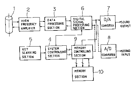
Referring to Fig. 2, the digital audio tape recorder
according to the present invention is constituted in such
a manner that signals reproduced from the head drum 1 are
amplified in a high frequency amplifier 2, converted to
parallel signals in a data processing section 3, digital-
filtered in a digital signal processing section 6 which
is controlled by a system controlling section 4,
converted to analog signals through digital-to-analog
converter 7 and outputted as aural signals. External
aural signals are also converted to digital signals
through an analog-to-digital converter 8, digital-
filtered in said digital signal processing section 6,
converted to serial signals in a data processing section
3, amplified in the high frequency amplifier 2, and then
applied to the head drum 1 as a recording signal. The
DAT system as shown in Fig. 2 according to the present
invention also comprises a memory section 10 for storing
signals that are inputted to said digital-to-analog
converter 7 from the said digital signal processing
section 6, and a memory controlling section 9 for storing
signals that are inputted to said digital-to-analog
converter 7 upon the control of the system controlling
section 4, and for reading and applying the signals
stored in said memory section 10 to said digital signal
processing section 6.
Fig. 3 is a block diagram showing a detailed
configuration for the system controlling section 4,
memory controlling section 9 and memory section 10 in
Fig. 2.
The DAT system as shown in Fig. 3 according to the
present invention is constituted so that the system
controlling section 4 receives key signals of a key
V,ll~
- 6 _ 2022219
scanning section 5 from a first microprocessor 41. Data
are exchanged in a deck controlling section 42 and the
microprocessor 41, an INDEX signal (ID), a READ signal
(RD), a WRITE signal (WR), an ENABLE signal (EN) and a
WRITE ENDING signal (WE) are outputted from the
microprocessor 41.
The DAT system also is arranged so that, under the
control of the signals (ID, RD, WR, EN, and WE) from the
microprocessor 41 of said system controlling section 4, a
second microprocessor 91 outputs chip selection signals
CSl-CS3, a READ/WRITE control signal (R/W) and a gate
signal (G), applies a BUSY signal indicating "in
operation~ to the first microprocessor 41. The data bus
(DB) of the microprocessor 41 is connected with said
digital signal processing section 6 when a GATE section
92 becomes conductive by the GATE signal (G) of the
second microprocessor 91.
On the other hand, the memory section 10 is
constructed so that each of the RAMs 101-103 is selected
by each of said chip select signals CSl-CS3 of the
microprocessor 91 of the memory controlling section 9,
and each of the 15 RAMs 101-103 are in a READ or WRITE
state by the READ/WRITE control signal (R/W) of the
microprocessor 91.
Fig. 4 is a flowchart for controlling the second
microprocessor 91 of the memory controlling section 9
with reception of key signals of the key scanning section
5 from the first microprocessor 41 of the system
controlling section 4, and Fig. 5 is a flowchart for
controlling the microprocessor 91 in the memory
controlling section 9.
202~21~
-- 7 --
Detailed description of the operations and effects
of the present invention will be given below with
reference to the flowcharts of Fig. 4 and Fig. 5.
At first, as shown in Fig. 4, key signals of the key
scanning section 5 are scanned in the microprocessor 41.
At this time, when a MEMORY key signal is inputted and a
memory flag is not set, the memory flag is set. If the
memory flag is set, the memory flag is cleared and the
ENABLE signal (EN) is initialized. At this time, the
READ signal (RD) is initialized if the WRITE signal (WR)
is not outputted. The WRITE ENDING signal (WE) is
outputted if the WRITE signal (WR) outputs and then said
WRITE ENDING signal (WE) and WRITE signal (WR) are
initialized when the BUSY signal is not applied from the
microprocessor 91 of the memory controlling section 9.
On the other hand, if the memory flag is set and the
memory key signal is not inputted, the system checks to
see whether a NUMBER key signal, a WRITE key signal and a
READ key signal are inputted and a function according to
the checked condition is performed.
That is, if the NUMBER key signal is inputted, the
number increases by "1". The number becomes "0" in case
that the number is more than 3, and the number is imme-
diately outputted as an INDEX signal (ID) in case of less
than 3. Thereafter, if the WRITE key signal is inputted
and the WRITE signal (WR) is not outputted, the READ
signal (RD) and the ~NART.~ signal (EN) are initialized
while the WRITE signal is outputted. Thereafter, when
the BUSY signal is not applied from the microprocessor 91
of the memory controlling section 9, the ENABLE signal EN
is outputted. This state is held during a writing stage
until the BUSY signal (BUSY) is not applied from the
microprocessor 91. On the other hand, when the READ key
signal is inputted and the writing is active, the ENABLE
" _..r~,i~
~P
2022~ 3
-- 8 --
signal (EN) is initialized and the WRITE ENDING signal
(WE) is outputted. Thereafter, when the BUSY signal
(BUSY) from the microprocessor 91 of the memory
controlling section 9 is not applied and the writing is
not active, the READ signal (RD) is outputted, the WRITE
signal is initialized, and the ENABLE signal (EN) is
outputted. This state is kept during a writing state
until the BUSY signal (BUSY) is not applied from the
microprocessor 91.
The READ signal (RD), the WRITE signal (WR) and the
~N~RT~ signal (EN) are all initialized when the BUSY
signal (BUSY) is not applied from the microprocessor 91
of the memory controlling section 9 with said WRITE and
15 READ states kept. As described above, the
microprocessor 91 of the memory controlling section 9
receives signals from the microprocessor 41 of the system
controlling section 4 and performs controls as in Fig. 5.
When a READ signal (RD) and an ENABLE signal are
inputted from the microprocessor 41, one of chip
selection signals CSl-CS3 corresponding to an INDEX
signal (ID) is outputted. A chip selection signal CSl is
outputted to select a RAM 101 if the INDEX signal (ID) is
"0", a chip selection signal CS2 is outputted to select a
RAM 102 if the INDEX signal (ID) is "1", and a chip
selection signal CS3 is outputted to select a RAM 103 if
the INDEX signal (ID) is "2". Thereafter, the BUSY
signal (BUSY), indicating "in operation", is outputted
from the second microprocessor 91 to be applied to the
first microprocessor 41, an address signal "0" is
outputted on the address bus (AR) to assign an address to
the RAMs 101-103 selected in the same manner as described
above, and a high potential GATE signal (G) is outputted
to turn the GATE section 92 on. At this time, the data
bus (DB) of the microprocessor 91 is connected with the
digital signal processing section 6.
2022219
g
The READ/WRITE control signal (R/W) is then
outputted at high potential from the microprocessor 91 to
change to the READ state the RAMs selected in the same
manner an described above, data recorded in a assigned
address as described above are read, and the data are
applied to the digital signal processing section 6
through the GATE section 92. Reading the data is
repeated with the address increased by "1" until the end
of the data and the highest address are met. When the
data fetching procedure is completed, the GATE signal (G)
is outputted in a low potential to cut off the GATE
section 92. At the same time, all of the chip selection
signals CSl-CS3 are outputted in a high potential, so
that RAMs 101-103 are not selected and the BUSY signal is
not outputted.
Meantime, if the WRITE signal (WR) and the ENABLE
signal (EN) are inputted to the microprocessor 91, the
chip selection signals corresponding to the INDEX signal
(ID) are outputted to select one RAM 101-103, a BUSY
signal indicating "in operation" is outputted to be
applied to the microprocessor 41 of the system
controlling section 4, an address signal of "0" is
outputted to the address bus (AB) and assign an address
of the RAM selected in the same manner as described
above, the GATE signal (G) of a high potential is
outputted to turn the GATE section 92 on.
Therefore, at this time, the data bus (DB) of the
microprocessor 91 is connected with the digital signal
processing section 6. Accordingly, at this time, signals
from the digital signal processing section 6 to the
digital-to-analog converter 7 are transferred to the
microprocessor 91 through the GATE section 92. At this
time, if the end of the data is not reached and the WRITE
ENDING signal (WE) is not outputted from the
microprocessor 41 as described above, the READ/WRITE
20222i9
-- 10 --
control signal (R/W) is outputted at low potential to
turn the RAM selected in the same manner as described
above to a WRITE state. The data read in the same manner
as described above are stored in the assigned address of
the selected RAM.
Thereafter, the READ/WRITE control signal (R/W) is
outputted at high potential and the address increases by
"1". As described above, the procedure which receives
and records the signals which are inputted to the
digital-to-analog converter 7 is repeated while the
address increases by "1" until the end of the data is met
or the WRITE ENDING signal (WE) is applied. Thereafter,
when the end of the data is met or the WRITE ENDING
signal is applied, the READ/ WRITE signal (R/W) is
outputted at low potential to store the end of the data
to the RAM selected in the same manner as described
above. Thereafter, the GATE signal (G) is outputted in a
low potential to cut off the GATE section 92. At this
time, all the chip selection signals CSl-CS3 are
outputted in a high potential, so that RAMs 101-103 are
not selected and the BUSY signal is not outputted.
Accordingly, as described above, while reproducing from a
tape, a MEMORY mode is made by the MEMORY key and the
WRITE key and a RAM is selected by the NUMBER key, so
that the reproduced signals are stored in the RAM.
When the DAT is in the RECORD mode, READ mode can be
made by the MEMORY key and READ key and a RAM is selected
by the NUMBER key, so that the signals stored in the RAM
can be recorded in a tape.
As described above in detail, the present invention
can duplicate a tape in one DAT with no use of an
additional DAT because, when the DAT is in a reproducing
mode, the reproduced signals are stored in the memory
section and the stored signals are read to record in a
~. ~
202221~
1 1 --
tape. The stored signals in the memory section can be
outputted as reproduced signals because the desired parts
of the signals are stored in the memory section.