Note: Descriptions are shown in the official language in which they were submitted.
2322238
A PROGR~MMARTT~ FAULT INSERTION CIRCUIT
CROSS REFERENCE TO RELATED APPLICATIONS
Cross Reference is made to the related U.S. Patent
Application entitled: "A PROGR~MMARLE FAULT INSERTION
ARRANGEMENT AND METHOD," (Docket 89-1-031), filed on the
same date, and by the same inventors as this Application.
FIELD OF THE lNv~NllON
The present invention relates to the field of
electronic test devices, and more particularly, to a
programmable device for inserting faults into an elec-
tronic digital circuit.
BACKGROUND OF THE INVENTION
Fault insertion is the means by which logic faults
are introduced into an electronic digital circuit. Logic
faults are operator induced logic signals such as a logic
"high" or logic "low" that are deliberately injected into
a digital electronic circuit. The circuit is then
monitored to ascertain if it responded correctly to the
fault. For example, in a digital circuit having the
capability to sense such failures and to send messages to
a controller, an inserted fault should solicit a trouble
message to the controller from the circuit. A failure to
send a trouble message would indicate a problem with the
maintenance functions of the circuit under test.
Additionally, faults may be inserted into a circuit under
test to ascertain how the circuit operates under the
faulted conditions.
Presently, fault insertion is a tedious manual
process carried out by a craftsperson or tec~n;cian. The
technician using jumper wire, or a similar tool, attaches
one end of the jumper to a connector pin of the device
under test and grounds the other end. In a digital logic
system this would simulate a logic "Low" or "0" state.
The tec-hnician would then monitor and interpret the
operating conditions of the circuit under test using
either a test terminal and monitor, an oscilloscope or
- 2022238
any other means commonly known for testing the
performance of digital circuits. The process is then
repeated for each fault inserted into the circuit under
test.
Manual fault insertion has disadvantages in that it
is extremely time consuming, and it is prone to human
error. Additionally, without special equipment only
logic "0" faults could be inserted into the circuit under
test. The logic "0" only fault insertion, tends to be
incomplete and therefore inefficient for the proper
testing of digital circuits.
Accordingly, it is an object of the present inven-
tion to provide a fault insertion circuit which can be
programmed by an operator to automatically apply fault
signals to a digital circuit under test.
DISCLOSURE OF THE INVENTION
The above and other objects, advantages, and
capabilities of the present invention are realized in a
fault insertion circuit arranged to generate and apply a
fault signal to a digital circuit under test.
The fault insertion circuit of the present invention
includes fault insertion hardware connected to the
digital circuit under test. The fault insertion circuit
includes a plurality of outputs with each output con-
nected to a respective input of the digital circuit under
test. The fault insertion hardware includes a plurality
of fault generating circuits, with each fault generating
circuit associated with a respective fault insertion
circuit o~ . A selection logic circuit is also
included for enabling a respective one of the fault
signal generating circuits.
A programmable controller is connected to the
selection logic circuit and is arranged under program
control to send control signals to the selection logic
circuit. A communication circuit is connected to the
controller circuit and to a data terminal, personal
2û22238
computer or any other source of programming commands and
instructions.
The communication circuit is arranged to receive the
commands and instructions from the data terminal and to
transmit the program commands and instruction to the
controller. The controller, in response to the received
program commands and instructions, transmits the appro-
priate selection control signals to the selection logic
circuit. The selection logic circuit then enables the
selected fault generating circuit applying the fault
signal to the digital circuit under test.
BRIEF DESCRIPTION OF THE DRAWINGS
A better understAn~ing of the invention may be had
from the consideration of the following detailed de-
scription taken in conjunction with the accompanying
drawings in which:
Figure 1 is block diagram showing the programmable
fault insertion circuit connected to a digital circuit
card under test in a digital system, in accordance with
the principles of operation of the present invention;
Figure 2 is a block diagram showing the major
functional areas of the programmable fault insertion
circuit, in accordance with the principles of operation
of the present invention; and,
Figure 3 is a detailed block diagram of the fault
insertion circuit, in accordance with the present
invention.
DESCRIPTION OF A PREFERRED EMBODIMENT
Directing attention first to Figure 1, depicted
therein, is the PLG~ammable Fault Insertion Circuit
(PFIC) in accordance to the principles of operation of
the present invention. As can be seen, the PFIC 10 is
connected between a Digital Circuit Card (DCC) 20, that
is to be tested and a Digital System (DS) 30. The DCC 20
is a functional subsystem of DS 30. A data terminal 40
is connected to the PFIC 10. The data terminal 40 is
~ 20~2238
used to issue commands to PFIC 10, in order to insert
faults into the DCC 20. A maintenance data terminal 50,
is connected to the DS 30 and is used to receive error or
warning messages sent by DS 50 in response to the PFIC 10
inserted faults. It is contemplated that the PFIC 10 is
connected between the DCC 20 and the backplane Bus of the
DS 50, via a pair of connectors (not shown) much in the
same manner as a circuit card extender.
With reference now to Figure 2, the major functional
areas of PFIC 10 will now be explained. The PFIC 10 is
comprised of three functional areas, the communication
port 11, the control hardware 12 and the fault insertion
hardware 13.
The communication port is used to receive and send
data from the data terminal 40. In the present embodi-
ment the communication port 40 utilizes the EIA RS232C
specification for communication between the PFIC 10 and
the data terminal 40. This provides for an industry
standard data connection between the PFIC 10 and the data
terminal 40 or a Personal Computer (PC). Therefore, any
PC having a RS232C serial interface can act as the data
terminal 40 to send and receive operating instructions to
the PFIC 10.
It will be appreciated by those skilled in the art
that other types of data communication standards or
protocols can be used to provide communication between
the PFIC 10 and the data terminal 40 and the present
invention is not limited thereto.
The control hardware 12 consists of the circuitry
which interprets and executes the data instructions and
commands sent to the PFIC 10 from the data terminal 40.
The commands perform diagnostics and induce or remove
faults. In this embodiment the control hardware is
comprised of a microcomputer of the type which includes
in single device a microprocessor, read only memory,
random access memory, timing, and I/O capabilities.
2022238
The fault insertion hardware is the functional
circuitry which under control of the control hardware
creates and applies to the selected connector pins of the
DCC 20 the requested faults.
The fault insertion hardware is configured to provide
the following fault types:
Stuck at 1 (S-A-l), a signal having a logic "1"
value;
Stuck at 0 (S-A-0), a signal having a logic "0"
value; and
Oscillation Fault, a signal which alternatively
pulled to a logic "0" and logic "1" state, creating a
square wave.
Referring now to Figure 3, a detailed explanation of
the programmable fault insertion circuit in accordance
with the present invention will now be given.
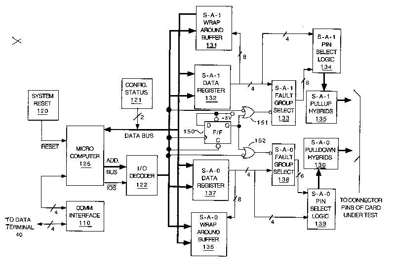
The communication interface 110 is comprised of a
RS232 Transmitter/Receiver (TR) circuit, which connects
the data terminal 40 to the serial communication ports of
controller 12. The RS232 TR circuit, uses an
asynchronous serial link, including a hAn~hAking
protocol, for transferring information to/from the
communication interface 110 and the data terminal 40.
The signals used by the TR circuit are: Data transmitted
(DT), Data Received (DR), Clear to Send (CTS) and Data
Terminal Ready (DTR). The interface is contemplated to
transfer information along the serial link at 9600 Baud
with each data byte composed of 7 bits of data, one even
parity bit, one start bit and one stop bit.
The control hardware 12 includes a microcomputer 125,
a system reset circuit 120, a configuration status
circuit 121, and a I/O decoder 122. The microcomputer
125 includes Read Only Memory (ROM), were the PFIC's 10
operating program is stored, Random Access Memory (RAM),
for the temporary storage of data, and a serial communi-
cation interface. The serial communication interface
2022238
_ connects the microcomputer 125 to the communications
interface 110.
The system reset circuit 120, powers up the the
microcomputer 125 properly, by providing a reset signal
that remains low for at least 20ms.
The configuration status circuit 121, is a hardwired
circuit which provides data to the microcomputer 125 that
identifies the type of PFIC 10 the microcomputer is
controlling. Since there are a great variety of circuit
cards with different connector pin configurations, such
as 98 pin upper/98 pin lower connector double height
cards, or 98 pin connector single height cards more than
one type of PFIC 10 must be produced and used.
Therefore, instead of generating two or more operating
programs to control each type of card, it is more
efficient to write a single operating program which can
control both types of PFICs. Thus, the microcomputer 125
checks which type of card it is installed on by reading
the configuration status circuit 121 and uses the
appropriate portions of the operating program for the
proper operation of PFIC.
The I/O decoder 122 is a single 3/8 decoder device
that is connected to the microcomputer's 125 address bus.
I/O decoder 122 decodes addresses generated by the
microcomputer 125 into control signals that enables the
fault insertion hardware within the I/O address space.
Signal IOS/ selects decoder 122 whenever a valid I/O
address appears on the address bus.
The fault insertion hardware consists of two groups
of identical components. The first group generates and
applies the S-A-l faults and the second group generates
and applies the S-A-0 faults. The first group includes
an S-A-l wrap around buffer 131, an S-A-l data register
132, an S-A-l fault group select 133, S-A-l pin select
logic 134, and S-A-l pullup hybrid devices 135. Simi-
larly, the second group includes an S-A-0 wrap around
.~
~ 3,
2022238
~-~ buffer 136, an S-A-0 data register 137, an S-A-0 fault
group select 138, S-A-0 pin select logic 139, and S-A-0
pulldown hybrid devices 130. Additionally, the fault
insertion hardware includes a diagnostic control flip
flop (F/F) 150, used to allow diagnostics to be run on
the fault insertion hardware.
The wrap around buffers 131 and 136 are connected to
the microcomputer's 125 data bus and are used during
diagnostics. When F/F 150 is set, the fault group select
decoders 133 and 138 are disabled allowing data written
to the data registers 132 and 137 to be read back to the
microcomputer via wrap around buffers 131 and 136. The
wrap around buffers 131 and 136 are enabled by signals
generated by the I/O decoder 122.
The data registers 132 and 137 are eight bit
register devices connected to the microcomputer's 125
data bus. Each register divides the stored data into an
upper and lower nibble (4 bits). The lower nibble is
used to select one of sixteen pins within the appropriate
S-A-l or S-A-0 fault group. The upper nibble selects one
of six appropriate S-A-l or S-A-0 fault groups. The data
registers are written to by the microcomputer 125 by an
enable signal generated by I/O decoder 122.
The fault group select decoders 133 and 138 receive
the upper nibble from its associated data register 132,
137 and generate an enable signal to one of the six fault
groups of the pin select logic devices 134, 139
respectively. The fault group select decoders 133, 138
are normally active unless deselected by gates 151 and
152 respectively, when diagnostics are run. Only one
fault group can be active at any one time.
Each pin select logic 134, 139 consists of six 4/16
decoders. Each decoder corresponds to a one of six fault
groups within the S-A-l and S-A-0 fault type. The
enabling signals generated by the group select decoders
selects one of the six pin select decoders. One of the
~c'`
2022238
sixteen pins of each decoder is then selected by the
deco~ing of the lower nibble of data from the associated
data register 132, 137. The pin select signal is then
applied to the associated pullup hybrid 135 or pulldown
hybrid 130.
The hybrid devices 135 and 130, are a plurality of
discrete transistor and resistor combinations which apply
the S-A-l or S-A-0 signals respectively, to the DCC 20.
Each transistor resistor combination receives an enabling
signal from its associated pin select decoder and
produces and applies the appropriate fault to the DCC 20.
With renewed reference to Figures 1 and Figure 3, an
explanation of the operation of PFIC 10 will now be
given. After the PFIC 10 is installed to the DCC 20 and
powered up, an initialization and diagnostics routine is
run by microcomputer 125. The microcomputer 125 issues
an address which is decoded by the I/O decoder 122. I/O
decoder 122 generates a set signal which is applied to
the clock input of F/F 150. The Q output of the now set
F/F 150, is applied to gates 151 and 152 which deselect
the S-A-l and S-A-0 fault group select decoders. The
microcomputer then writes a byte of data into each of the
data registers 132, 137. After the data has been written
to the data registers 132, 137 the microcomputer 125 via
the appropriate wrap around buffer 131, 136 reads the
data back and checks that the data read back is correct.
If the data read back is correct the I/O decoder 122
generates a reset signal which is applied to the C
(clear) input of F/F 150, resetting the fault insertion
hardware for normal operation. The diagnostic routines
also check the microcomputer 125 RAM space, a checksum of
the program ROM and the integrity of the communication
link, by checking for even parity on the incoming data.
Any hardware failures are stored as data in the
microcomputer's 125 RAM and transmitted to the data
terminal 40 as a response to a prompt request.
2022238
-~ The fault generation and insertion sequence between
data terminal 40 and the PFIC 10 begins when the data
terminal 40 issues a command to PFIC 10 requesting a
prompt. If all diagnostics are sllcc~scfully completed,
the PFIC 10 sends to the data terminal 40 a character
describing the PFIC 10 card type. This data is read by
the microcomputer 125 from the configuration status
circuit 121. If the PFIC 10 fails diagnostics a charac-
ter is returned indicating hardware problem.
If a valid prompt is sent to the data terminal 40
from the PFIC 10, the data terminal 40 then transmits a
command to the PFIC 10 to induce a fault. The command
between the data terminal 40 and the PFIC 10 has the
following structure:
I - Command Type, this could either be I (Insert) or
R (reset).
1 - Card number, refers to the number of card under
test addressed.
U - Sector, refers to the portion of the card under
test where the pin to be faulted is located. This
could be U (upper) or L (lower) for a double height
card, or S (single) for a single height card.
00 - Pin number, refers to number of the pin to be
faulted.
H - Fault type, refers to the type of fault to be
inserted; H (high), L (low) or O (oscillation).
0000 - Duration time, refers to the length of time,
in milliseconds, a high or low fault is to be
maintained.
0000 - High time, refers to the length of time, in
milliseconds, an oscillation fault is to remain
high.
0000 - Low time refers to the length of time, in
milliseconds, an oscillation fault is to remain low.
.~
`-- 2022238
Using the command structure just described, a fault
can be induced into the DCC 20 by transmitting to the
PFIC 10 the following command message.
I 1 S 10 H 0025 0000 0000
This command message will insert a S-A-1 signal on pin
number ten of the DCC 20 having a duration of 25ms.
The transmitted message is read and interpreted by
the microcomputer 125, which sends an appropriate address
to the I/0 decoder 122. The decoder 122 enables the
correct data register, in this example the S-A-l data
register 132 and the fault group select decoder 133.
The microcomputer 125 sends over the data bus a byte
of data containing the fault group select and pin select
data to the S-A-1 data register 132. After the data is
read into the data register 132, the lower nibble of the
data byte is transmitted to the S-A-l pin select logic
134, and the higher nibble sent to the S-A-l fault group
select 133. The higher nibble is decoded by fault group
select 133 and the appropriate decoder of the pin select
logic 134 is enabled. The enabled pin select logic
decoder 134 reads the low order nibble and the pullup
hybrid associated with the DCC 20 pin number 10 is
activated to induce a S-A-l fault for the commanded
duration time.
When the time duration is completed the fault is
removed and a command completed response is transmitted
to the data terminal 40 from the PFIC 10. The PFIC is
then ready to accept another fault insertion command from
the data terminal 40. The results of the fault induced
into the DCC 20 can then be monitored via the DS 30
maintenance data terminal 50.
It is, however, useful to underscore some of the
salient attributes of the subject invention. It will be
well understood by those skilled in the art that the
present invention provides for the ability to communicate
with a data terminal or a PC to automatically insert
2022238
~,
faults under the terminal's or PC's direction. The
insertion can be under the direction of an operator or
under the direction of a program written to execute a
specific sequence of faults into the digital system. The
present invention easily allows a technician to write a
test plan which would run on a PC, that would
automatically insert faults into the digital system
hardware and collect the test data to be analyzed at a
later time or date.
Furthermore, it will be obvious to those skilled in
the art that numerous modifications to the present
invention can be made without departing from the scope of
the invention as defined by the appended claims. In this
context, it should be recognized that the essence of the
invention resides in a fault insertion circuit which can
be programmed by an operator, a data terminal or a
personal computer to automatically apply a plurality of
faults into a digital system, in order to ascertain if
the digital system is operating properly.